國
立
交
通
大
學
電子工程學系 電子研究所
碩
士
論
文
實現在 40 奈米製程下可應用於 IP 位址搜尋之
高能源效益三態內容可定址記憶體電路設計
Energy-Efficient TCAM Design for IP Lookup Tables
in 40nm LP CMOS Process
研 究 生:賴淑琳
指導教授:黃 威 教授
實現在 40 奈米製程下可應用於 IP 位址搜尋之
高能源效益三態內容可定址記憶體電路設計
Energy-Efficient TCAM Design for IP Lookup Tables
in 40nm LP CMOS Process
研 究 生:賴淑琳 Student:Shu-Lin Lai
指導教授:黃 威 教授 Advisor:Prof. Wei Hwang
國 立 交 通 大 學
電 子 工 程 學 系 電 子 研 究 所
碩 士 論 文
A Thesis
Submitted to Department of Electronics Engineering & Institute of Electronics College of Electrical Engineering and Computer Engineering
National Chiao Tung University in partial Fulfillment of the Requirements
for the Degree of Master in Electronics Engineering September 2012 Hsinchu, Taiwan
中華民國一○一年九月
實現在 40 奈米製程下可應用於 IP 位址搜尋之
高能源效益三態內容可定址記憶體電路設計
學生:賴淑琳
指導教授:黃 威 教授
國立交通大學電子工程學系電子研究所
摘 要
即便三元內容可定址記憶體是個大功耗的晶片系統設計,但仍被廣泛地應用 在 IP 位址搜尋之功能上。在本論文中,提出了實現在 40 奈米製程下高能源效益 的可定址記憶體電路設計。由於先進製程底下 N 極電晶體的導通電流小,在 16 電晶體三元內容可定址記憶體中,我們採用 P 極的比較電路來增加動態電路的導 通電流。另外,使用 AND 閘連接的蝴蝶式比較線連結架構不僅能降低動態節點 的導線電容,也能確保每一子節的動態節點電容量為相同。為了進一步降低功率 的消耗,我們提出了漣波位元線讀取架構及漣波比較傳輸架構,並且結合可定址 記憶體內無關項的特性。比起傳統階層式架構,它同時降低了比較傳輸線的切換 功率也節省了位元線和比較傳輸線的長導線電容。此外,我們提出了垂直式資料 感測電路來加強寫入能力;另一方面,藉由無關項特性的動態電源電路設計來縮 減漏電流和提高靜態雜訊邊界。寫入時,為了避免所儲存的資料被破壞及提升資 料感測控制電路對環境變異的穩定性,在我們設計當中也提供了複製電路來控制 動態電源的開關時間。建立在 40 奈米製程上,我們結合這多項低功耗電路架構 實現在 256x40 和 256x144 的三元內容可定址記憶體中。經由電路佈局後的模擬 顯示,操作在 400 百萬赫茲及 1 伏特電壓底下,可省 28.9%的漏電功耗和 31.74% 的比較傳輸線功耗,並且平均每個可定址記憶體也只消耗 0.461 飛焦耳。Energy-Efficient TCAM Design for IP Lookup Tables
in 40nm LP CMOS Process
Student: Shu-Lin Lai
Advisors: Prof. Wei Hwang
Department of Electronics Engineering & Institute of Electronics
National Chiao-Tung University
ABSTRACT
Ternary content addressable memory (TCAM) is extensively adopted in routing tables of network systems and occupied great amounts of energy consumption. In this thesis, energy-efficient TCAM macros have been designed and realized in 40nm LP CMOS process with the sizes of 256x40 and 256x144, respectively. Based on the small drain current in 40nm LP CMOS process, a 16T AND-type TCAM cell with p-type comparison circuits is utilized to increase the Ion/Ioff ratio of the dynamic circuitry. Additionally, the butterfly match-line
scheme with AND gates is designed to reduce the wire loading on the evaluation nodes and to ensure that the capacitance of the evaluation nodes are the same in all segments. For further reducing the energy consumption in nano-scale technologies, don’t-care-based ripple search-line and ripple bit-lines are realized to decrease both the switching activities and wire capacitance of search-lines and bit-lines. Moreover, the column-based data-aware power control is also employed to realize the leakage power reduction, write-ability and static noise margin (SNM) improvements by the power gating devices. Consequently, the timing of the power switching is tolerant to PVT variation and Vt scatter by the replica circuitry. The energy-efficient 256x40 and 256x144 TCAM macros are implemented using UMC 40nm LP CMOS technology, and the experimental results demonstrate a leakage power reduction of 28.9%, a search-line power reduction of 31.74% and an energy metric of the TCAM macro of 0.461 fJ/bit/search.
誌 謝
可以完成這篇論文,要感謝的人很多很多。首先,我要感謝指導教授黃威教 授,在老師的帶領下讓我學會研究時正確的態度跟方法,也時時指引著我正確的 研究方向。另外,老師更提供了良好的研究環境和充足的資源,讓我能充分發揮 自己的能力完成這篇論文。接著,我要感謝莊景德教授經常給予我許多研究內容 的指導,同時產學合作的計畫也讓我得到許多意外的收穫。 再者,要感謝指導我的學長黃柏蒼,在研究的這一路上不停地給予我新觀點 跟方向讓我學習,遇到困難時也會不厭其煩的指導我渡過難關。此外也感謝張銘 宏、楊皓義及謝維致這三位博班學長們的幫助及討論。當然還要感謝實驗室夥伴 林弘璋及陳美維,這一路上的相互扶持跟鼓勵,也是我在碩班研究生活上的一大 助力,在此一併感謝。 最後要感謝最親愛的父母親跟姐姐,總是在我面對挫折或感到疲憊時給予我 最大的鼓勵和支持,適時的關懷更使我有無比的動力繼續前進,才能夠順利完成 碩士的論文研究。另外,也感謝許多好朋友們,總是在背後支持著我,成為我心 靈最重要的支柱。在這邊無法用有限的文字表達無限的感謝,但淑琳真心誠意的 感謝大家。
Contents
Chapter 1 Introduction ... 1
1.1 Background ... 1
1.2 Motivation ... 2
1.3 Thesis Organization ... 3
Chapter 2 Overvuew of Low Power CAM/TCAM Design ... 5
2.1 Applications & Architecture of CAM/TCAM ... 5
2.1.1 Conventional CAM Architecture ... 5
2.1.2 Applications of CAM/TCAM ... 7
2.1.2.1 Cache Memory ... 7
2.1.2.2 Translation Look-aside Buffer ... 8
2.1.2.3 ATM Switches ... 10
2.1.2.4 Packet Forwarding Using CAM... 11
2.2 Design of CAM/TCAM Cells ... 12
2.2.1 Binary CAM Cell ... 12
2.2.1.1 NOR-type CAM Cell ... 13
2.2.1.2 AND-type CAM Cell ... 14
2.2.2Ternary CAM Cell ... 15
2.2.2.1 NOR-type TCAM Cell ... 15
2.2.2.2 AND-type TCAM Cell ... 17
2.3 Low Power Match-Line Scheme ... 18
2.3.1 Conventional Match-line Structure ... 19
2.3.1.1 NOR-type Match-line ... 19
2.3.1.2 AND-type Match-line ... 20
2.3.2 Selective Pre-charge Scheme ... 21
2.3.3 Pipelined Hierarchical Search Scheme ... 22
2.3.4 Current-Saving Scheme ... 23
2.3.5 Wide-AND Match-line Scheme ... 24
2.3.6 Tree Style AND-type Match-line Scheme ... 25
2.4 Low Power Search-line Schemes... 27
2.4.1 Hierarchical Search-line Scheme ... 27
2.4.2 Charge-Recycling Search-line Scheme ... 29
2.4.3 Two-Level Don't-Care Gating Scheme ... 30
2.4.4 Low Swing Search-line Scheme ... 31
2.5 Low Power Design Techniques for CAM/TCAM Macro ... 32
2.5.1 Power-Gated ML Sensing ... 32
2.5.3 Dynamic Power Source (DPS) Technique ... 36
2.5.4 Variability-Tolerance CAM Cells with NOR-type Match-lines ... 37
Chapter 3 Energy-Efficient Match-Line Schemes ... 39
3.1 Conventional NAND-Type Match-Line Schemes ... 39
3.2 And-Type TCAM Cell with P-Type Comparison Circuits ... 42
3.3 XOR-based Conditional Keeper ... 45
3.3.1 Circuit Implementation ... 45
3.3.2 Design Analysis ... 47
3.4 Butterfly Match-Line Scheme... 48
3.4.1 Organization ... 49
3.4.2 Design Consideration ... 51
3.5 Summary ... 53
Chapter 4 Column-Based Low Power Design Techniques ... 55
4.1 Ripple Bit-Line Scheme for Read/Write Operation ... 56
4.1.1 Circuit Implementation & Operation ... 56
4.1.2 Design Consideration ... 58
4.2 Don't-Care-Based Ripple Search-Line Scheme ... 60
4.2.1 Circuit Implementation ... 60
4.2.2 Design Consideration ... 62
4.3 Column-Based Data-Aware Power Control ... 64
4.3.1 Basic Concept ... 65
4.3.2 Replica Timing Control Circuit ... 69
4.4 Simulation Results and Analysis ... 71
4.4.1 Performance Comparison of HSL and RSL ... 71
4.4.2 Simulation Result for DAPC ... 75
4.5 Summary ... 77
Chapter 5 Implementation of 256x40 and 256x144 Energy-Efficient
TCAM Macro in UMC 40nm LP CMOS process ... 78
5.1 Specification of Energy-Efficient TCAM Macro ... 78
5.2 Architecture & Floor-planning of TCAM Macro ... 82
5.3 Butterfly Match-Line Design for 256x40 and 256x144 ... 85
5.4 Design Implementation in UMC 40nm LP CMOS Process ... 87
5.4.1 Shared BL/DL ... 87
5.4.2 Interleaving Vertical Lines ... 88
5.4.3 Cell Layout... 90
5.5 Simulation Results and Analysis ... 91
5.5.1 Simulation Results of 256x144 TCAM Macro ... 91
5.6 Summary ... 96
Chapter 6 Conclusions and Future Works ... 98
6.1 Conclusions ... 98 6.2 Future Work ... 99
Bibliography ... 102
Chapter 1 ... 102 Chapter 2 ... 103 Chapter 3 ... 109 Chapter 4 ... 110 Chapter 5 ... 111Vita ... 113
List of Figures
Fig. 1.1 Binary CAM (BCAM) cell and ternary CAM (TCAM) cell. ... 1
Fig. 2.1 Conventional CAM architecture. ... 6
Fig. 2.2 A simple cache memory. ... 8
Fig. 2.3 A simple virtual memory system. ... 9
Fig. 2.4 ATM switch with CAM. ... 10
Fig. 2.5 Packet forwarding by an address-lookup table in network routers. ... 11
Fig. 2.6 NOR-type binary CAM cell. (a) 9T BCAM cell and (b) 10T BCAM cell. ... 13
Fig. 2.7 AND-type 9-transistor binary CAM cell. ... 14
Fig. 2.8 Static NOR-type ternary CAM cell. ... 15
Fig. 2.9 Dynamic NOR-type ternary CAM cell. ... 17
Fig. 2.10 AND-type ternary CAM cell. ... 17
Fig. 2.11 Structure of conventional NOR-type match-line. ... 19
Fig. 2.12 Structure of conventional AND-type match-line. ... 20
Fig. 2.13 Word structure of the selective pre-charge scheme. ... 22
Fig. 2.14 Pipelined MLs reduce power by shutting down after a miss in a stage 23 Fig. 2.15 Current-saving match-line sensing scheme ... 23
Fig. 2.16 64 bits sequential AND plan and HS-AND match circuit. ... 25
Fig. 2.17 (a) Parallel, (b) 3-level tree, and (c) 2-level tree AND-type match lines. ... 26
Fig. 2.18 Schematic of the hierarchical search-line architecture. ... 28
Fig. 2.19 Charge-recycling search-line driver ... 29
Fig. 2.20 (a) L1 gating node (GNL1) implementation. (b) L2 DCG example .... 30
Fig. 2.21 Operation of a NOR-cell in the LSSL-CAM. (a) Mismatch. (b) Match. ... 31
Fig. 2.22 Schematic of the NOR-cell block in the LSSL_CAM. ... 31
Fig. 2.23 Row-based ML sense amplifier and new CAM architecture. ... 33
Fig. 2.24 The differential NAND CAM cell. The block M and block DMLSA denote a memory cell to store the data bit and differential ML sense amplifier .. 34
Fig. 2.25 DMLSA. ... 35
Fig. 2.26 (a) DPSVDD implementation. (b) DPSGND implementation. ... 36
Fig. 2.27 (a) NVT-BCAM cell with NOR-type match-line. (b) Read/Write timing sequence of the NVT-BCAM cell. ... 37
Fig. 3.2 Transfer dynamic logic into clock-and-data pre-charge dynamic (CDPD)
circuits. ... 41
Fig. 3.3 Pseudo-footless clock-and-data pre-charge dynamic (PF-CDPD) circuits. ... 41
Fig. 3.4 16T AND-type TCAM cell with P-type comparison circuits. ... 43
Fig. 3.5 Drain current versus gate voltage for different technology. ... 44
Fig. 3.6 AND-type match-line with XOR-based conditional keeper. ... 45
Fig. 3.7 The diagram of XOR-based conditional keeper. ... 46
Fig. 3.8 (a) Search time (b) Power consumption versus UNG margin for different keepers. ... 47
Fig. 3.9 Butterfly match-line scheme. ... 49
Fig. 3.10 Modification of NOR gate in TCAM segment. ... 52
Fig. 3.11 Butterfly connection style with P-type comparison circuit and XOR-based conditional keeper. ... 54
Fig. 4.1 Packet routing based on longest prefix matching mechanism ... 55
Fig. 4.2 The ripple bit-line scheme and timing waveforms of read operation. .... 57
Fig. 4.3 Power and delay comparisons of the local bit-line scheme. ... 59
Fig. 4.4 (a) A simplified architecture (b) Circuit implementation of don’t-care based ripple search-line scheme... 61
Fig. 4.5 Delay of ripple search-line scheme versus number of TCAM cells on each local search-line. ... 63
Fig. 4.6 The architecture of column-based data-aware power control in TCAM macro... 65
Fig. 4.7 Cell connection of column-based data-aware power control scheme. ... 66
Fig. 4.8 Control Circuits for (a) storage cells (b) don’t-care cells. ... 67
Fig. 4.9 An adaptive replica timing control circuit for data-aware scheme. ... 69
Fig. 4.10 The diagram of adaptive write-time tracing replica. ... 70
Fig. 4.11 (a) Hierarchical search-line structure. (b) Ripple search-line structure. ... 71
Fig. 4.12 Search-line power consumption under different don’t-care patterns. .. 73
Fig. 4.13 Analysis of the search-line delay under different search-line schemes. ... 74
Fig. 4.14Leakage power consumption under different don’t-care pattern when Flag=1. ... 75
Fig. 4.15 Leakage power consumption under different don’t-care pattern when Flag=0. ... 76
Fig. 5.1 Timing diagram of writing storage/don’t-care cells. ... 81
Fig. 5.2 Timing diagram of reading storage/don’t-care cells. ... 82
Fig. 5.3 Timing diagram of search operation. ... 82
Fig. 5.4 Block diagram of 256x40 TCAM macro. ... 83
Fig. 5.5 The floor-plan of energy-efficient 256x40 TCAM macro. ... 84
Fig. 5.6 Butterfly match-line scheme for 144-bit TCAM cells. ... 85
Fig. 5.7 (a) Two-stage (b) Three-stage butterfly match-line scheme for 40-bit TCAM cells. ... 86
Fig. 5.8 (a) Typical TCAM cell. (b) TCAM cell with shared BL/DL. ... 87
Fig. 5.9 Coupling capacitance. ... 88
Fig. 5.10 (a) Coupling Effect of conventional vertical lines. (b) Interleaving vertical lines. ... 89
Fig. 5.11 Layout view of 1-bit TCAM cell. ... 91
Fig. 5.12 Timing analysis of search operation. ... 92
Fig. 5.13 Layout view of a TCAM segment with 5-bit TCAM cells ... 93
Fig. 5.14 A 256x40-bit layout of the proposed energy-efficient TCAM. ... 94
List of Tables
Table 2.1 Truth table of NOR-type binary CAM cell. ... 13
Table 2.2 Truth table of AND-type binary CAM cell. ... 15
Table 2.3 State assignments and truth table for static TCAM cell. ... 16
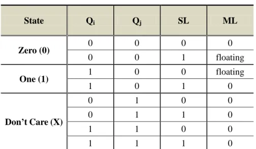
Table 2.4 State assignments for TCAM cell. ... 18
Table 3.1 Control organism of XOR-based conditional keeper. ... 45
Table 3.2 Comparison of search delay with NOR gate and AND gate in TCAM segment (Unit: ns). ... 53
Table 4.1 Key signals of replica-column scheme. ... 58
Table 4.2 The corresponding virtual source voltage under different operations.. 66
Table 4.3 The truth table of the control signals for storage cells. ... 68
Table 4.4 The truth table of the control signals for don’t-care cells. ... 69
Table 5.1 Descriptions of input pins. ... 79
Table 5.2 Descriptions of output pins. ... 80
Table 5.3 Truth table of three modes. ... 81
Table 5.4 Pre-simulation result of 256x144 TCAM macro. ... 93
Table 5.5 Summary of the 256x144 TCAM macro ... 93
Table 5.6 Post simulation result of 256x40 TCAM macro. ... 95
Chapter 1
Introduction
1.1 Background
Content-addressable memory (CAM), also called associative memory, executes the
lookup-table function in a single clock cycle using dedicated comparison circuitry.
CAM compares input search data against a table of stored information, and returns the
matching data. Accordingly, CAM cells contain storage memories and comparison
circuits. CAM cells are of two types – binary content addressable memory (BCAM)
and ternary content addressable memory (TCAM) - depending on their comparison
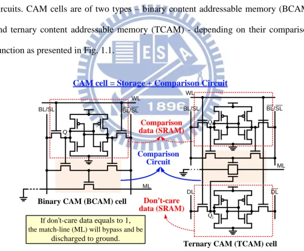
function as presented in Fig. 1.1.
ML WL BL/SL BL/SL i Q WL BL/SL BL/SL DL DL ML Qi Qj Comparison Circuit Comparison data (SRAM)
CAM cell = Storage + Comparison Circuit
Binary CAM (BCAM) cell
Ternary CAM (TCAM) cell
Don't-care data (SRAM) If don't-care data equals to 1,
the match-line (ML) will bypass and be discharged to ground.
Fig. 1.1 Binary CAM (BCAM) cell and ternary CAM (TCAM) cell.
A BCAM cell has two states – the “one” state and the “zero” state. A BCAM cell
- logic 0, logic 1, and don’t-care X. The third state, don’t-care X, which is used in
masking, makes TCAM suitable for network router applications. Hence, the
difference between BCAM and TCAM is that TCAM contains an extra SRAM to
store the don’t-care state. If the datum in don’t-care cell is 1, then the match-line (ML) will bypass the don’t-care cells and be discharged to ground. It will not perform any comparison operation. If the datum in don’t-care cell is 0, then the function of TCAM is the same as that of BCAM.
Due to fast search capability, CAM has been employed in numerous applications
requiring high search speed. In past decades, these applications are parametric curve
extraction [1.1], Hough transformation [1.2], Lempel–Ziv compression [1.3], image
coding [1.4], the human body communication controller [1.5], the periodic event
generator [1.6], and the virus-detection processor [1.7]. At present, CAM is popular
for use in network routers for packet forwarding, packet classification, asynchronous
transfer mode (ATM) switching, and other functions.
1.2 Motivation
As the range of CAM applications grows, power consumption is one of the critical
challenges. The trade-off among power, speed, and area is the most important issue in
recent researches on large-capacity CAMs. The primary commercial application of
CAMs today is the classification and forwarding of Internet protocol (IP) packets in
network routers. To overcome the dwindling unallocated address space. Internet
Protocol Version 6 (IPv6) becomes mandatory to build new Internet networks and
services. The IP address space is expanded from 32-bit to 144-bit identifiers for
interfaces and set of interfaces [1.8]-[1.11]. With existing implementations ranging
network routers for packet forwarding applications. Accordingly, high speed and low
power are the two major goals of TCAM design for IP-address forwarding
applications, especially in nano-scale technologies.
With the silicon technology entering the sub-65nm regime, the leakage power
increasingly dominates the overall power consumption. However, previous
investigations of low-power TCAM have focused only on dynamic power
consumption [1.12]-[1.15]. The data-aware power control scheme is proposed for
reducing both the leakage current and dynamic power dissipation and further
improving write-ability. The other serious issue, Ion-Ioff-ratio, is expected to further
worsen with technology scaling, resulting the degradation of search performance and
TCAM cell functionality, particularly in low power process. We have developed the
AND-type TCAM cell with P-type comparison circuit to conquer these problems.
For high density circuit design, the ripple bit-line scheme and ripple search-line
scheme are proposed to not only enhance the area efficiency but also save additional
process cost for hierarchical lines layer. Based on continuous don’t-care pattern, the
don’t-care-based ripple search-line scheme also reduces dynamic power effectively.
Moreover, the noise-tolerant XOR-based conditional keeper and butterfly match-line
scheme are adopted to further reduce the power consumption and the length of critical
paths [1.16]. In this work, a 256x40 and 256x144 TCAM macros are implemented
using UMC 40nm low power technology. The details of energy-efficient techniques
and analysis are also included.
1.3 Thesis Organization
word schemes would be presented. Besides, the application and prior low power
methodologies of CAM would be described in this chapter as well. The noise-tolerant
butterfly match-line scheme with XOR-based conditional keeper is realized in
Chapter 3. Furthermore, AND-type TCAM cell with P-type comparison circuit also
described. Chapter 4 presents the ripple bit-line scheme, don’t-care-based ripple
search-line scheme and data-aware power control scheme. By utilizing the regular
table of don’t-care pattern, both the dynamic and leakage power can be saved. The
energy-efficient 256x40 and 256x144 ternary CAM array are implemented in Chapter
5. In this chapter, other layout considerations are presented to reduce area overhead
and coupling effect, including shared BL/DL and interleaving vertical global lines
techniques. Finally, the overall investigation results and conclusions are drawn in
Chapter 2
Overview of Low Power CAM/TCAM
Design
This chapter is a study of CAM-design technique at the circuit level and at the
architectural level. Typically CAM/TCAM architecture and the applications will be
described in section 2.1. The basic operation, cell circuits and word schemes of CAM
are presented in section 2.2. The low power match-line schemes and low power
search-line driving approaches are presented in section 2.3 and 2.4, respectively. At
the architecture level, section 2.5 reviews several design techniques for reducing
power consumption of CAM/TCAM macro.
2.1 Applications & Architecture of CAM/TCAM
2.1.1 Conventional CAM Architecture
A conventional CAM architecture is usually composed of the data memories,
address decoders, bit-lines pre-charge circuits, word match schemes, read sense
amplifiers, address priority encoders and so on [2.1]-[2.7]. Fig. 2.1 shows a simplified
block diagram of a CAM. Generally, CAM has three operation modes: write, read,
and search. In write and read operation, CAM plays just like an ordinary memory.
That is to say, data is manipulated in the CAM array as the same way in SRAM array.
Different from SRAM, CAM has a special mode: search mode. The input in Fig. 2.1
called search word that is broadcast onto the search-lines to the table of stored data.
The number of bits in a CAM word is usually large, with existing implementations
few hundred entries to 32K entries, corresponding to an address space ranging from 7
bits to 15 bits. Each stored word has a match-line that indicates whether the search
word and stored word are identical (the match case) or are different (a mismatch case,
or miss). The match-lines are fed to an encoder that generates a binary match location
corresponding to the match-line that is in the match state. An encoder is used in
systems where only a single match is expected. In CAM applications where more than
one word may match, a priority encoder is used instead of a simple encoder. A priority
encoder selects the highest priority matching location to map to the match result, with
words in lower address locations receiving higher priority. The overall function of a
CAM is to take a search word and return the matching memory location. One can
think of this operation as a fully programmable arbitrary mapping of the large space
of the input search word to the smaller space of the output match location.
Address Input Address Output A d d re s s D e c o d e r
Memory Cell Array n words x m bits
Bit Line Prechargers
W o rd M a tc h C ir c u it s A d d re s s P ri o ri ty E n c o d e r Data
Input Data Lines
Read Sense Amps. Data Output Read enable Write enable Search word Reset CLK
2.1.2 Applications of CAM/TCAM
CAMs are widely used in cache memory system and translation look-aside buffer
(TLB) in virtual memory system in past years. The primary commercial application of
CAMs today is to classify and forward Internet protocol (IP) packets in network
routers [2.8]-[2.12]. In networks like the Internet, a message such an as e-mail or a
Web page is transferred by first breaking up the message into small data packets of a
few hundred bytes, then sending each data packet individually through the network.
These packets are routed from the source, through the intermediate nodes of the
network (called routers), and reassembled at the destination to reproduce the original
message. The function of a router is to compare the destination address of a packet to
all possible routes, in order to choose the appropriate one. A CAM is a good choice
for implementing this lookup operation due to its fast search capability.
2.1.2.1 Cache Memory
In the memory hierarchy system, cache plays an important role [2.13], [2.14].
Cache is the name given to the first level of the memory hierarchy encountered once
the address leaves the CPU. Its function is used to refer to any storage managed to
take advantage of locality of access. Cache serves as a method for providing fast
reference to recently used portion of instruction or data. When CPU finds a wanted
data item in the cache, it is called cache hit. On the contrary, if CPU does not find a
data item that is needed in the cache, it is called cache miss.
An example for direct data mapping cache is illustrated in Fig. 2.2. The address
can tell us the capacity of cache. If there are N bits for Index, the cache has 2N entries
which can be stored data items. The action is first to find the corresponding position
of index. When the corresponding position is found out, the tag stored in the
corresponding position would be taken out. This tag would be compared to the third
part of tag. If they are the same, and valid bit is one, a hit signal and the
corresponding data would be sent out. Of course, the tag entries are composed of
CAM array. The valid bit is used to indicate whether an entry contains a valid address
or not. If they are not the same, a miss occurs.
Fig. 2.2 A simple cache memory.
2.1.2.2 Translation Look-aside Buffer
Translation look-aside buffer (TLB) is widely used to virtual memory system. A
TLB is like a cache that hold only page table mapping [2.13], [2.14]. Its function is to
provide fast translation from the virtual address to the physical address. When we get
Valid Tag Data
31 30 ……… 13 12 11 ……2 1 0
=
hit data 20 10 20 32 Index 0 1 2 3 1022 1023 Index Tagthe physical address, we can use this physical address to access the data which are
stored in the memory (such as cache or DRAM or DISK). Because TLB can speed up
address translation in processor with virtual memory and it also can cut down access
time and lowering the miss rates.
Fig. 2.3 A simple virtual memory system.
Fig. 2.3 shows a simple virtual memory system. The TLB contains a subset of the
virtual-to-physical page mappings that are in the page table. Because the TLB is a
cache, it must have a tag field which consists of CAMs. As a virtual page number
(VPN) is sent to the TLB, this VPN would be compared with all valid tags in TLB. If
the VPN can find a corresponding tag in the TLB, the corresponding physical page
address would find in the corresponding tag. However, if there is no matching entry in
the TLB for a page, the page table must be examined. The page table either supplies a
physical page number for the page or indicates that the page resides on disk, in which
case a page fault occurs. Since the page table has an entry for every virtual page, no 1 1 0 1 1 0 1 1 1 0 1 1 1 0
Valid Tag Physical page address
TLB Page table Valid Physical page or disk address 1 1 1 0 1 VPN Physical memory Disk storage
tag field is needed.
2.1.2.3 ATM Switches
For ATM switching network application, CAM can be adopted as a translation
table. Virtual circuits are important parts to ATM networks, and they need to be set up
across ATM networks before any data transfer because ATM networks are
connection-oriented. There are two types of ATM virtual circuits, Virtual Path
(identified by a virtual path identifier [VPI]) and Channel Path (identified by a
channel path identifier [VCI]). Each segment of the total connection has unique
VPI/VCI combinations, and the VPI/VCI value of ATM cells would be changed into
the value for the next segment of connection while ATM cell go through a switch
[2.15], [2.16]. Data VCI 17
CAM
PC 46738987
RAM
Address VCI 24 VCI 05 Address 2 0 1 VCI 48 VCI 05 … 3 4 ... Address 2 0 1 Data VCI 17 VCI 24 VCI 05 3 4 … VCI 48 85 ...ATM Switch
Current Connection
Next Connection
VPI/VCI
Fig. 2.4 ATM switch with CAM.
CAM is applied to an ATM switch as an address translator and can quickly
perform the VPI/VCI translation. In the translation process, the CAM causes address
CAM/RAM combination realizes the multi-megabit translation tables with full
parallel search capability. Take VPI/VCI fields from the TM cell header and the list of
current connections stored in the CAM array for comparison, as a result, CAM
originates and address which is used to access an external RAM where VPI/VCI
mapping data and other connection information is stored. The ATM controller uses the
VPI/VCI data from the RAM for modifying the cell header, and the cell is sent to the
switch, depicted in Fig. 2.4.
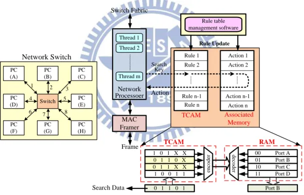
2.1.2.4 Packet Forwarding Using CAM
1 0 1 X X 0 1 1 0 X 0 1 1 X X 1 0 0 1 1 en co d er 0 1 1 0 1 TCAM 00 Port A 01 Port B 10 Port C 11 Port D d ec o d er Port B RAM Search Data Thread 1 Thread 2 Thread m Network Processoer MAC Framer Frame Switch Fabric Rule table management software Network Switch Rule Update Rule 1 Rule 2 Rule n-1 Rule n Action 1 Action 2 Action n-1 Action n TCAM Associated Memory Search Key Action Switch PC (B) PC (G) PC (D) PC (A) PC (F) PC (E) PC (C) PC (H) 1 2 3 4 5 6 7 8
Fig. 2.5 Packet forwarding by an address-lookup table in network routers.
In recently years, TCAMs have been popularly used in network routers for packet
forwarding and packet classification. Network routers forward data packets from an
incoming port to an outgoing port, using an address-lookup function [2.17]-[2.20]. Fig.
output port associated with that address. The router maintains a list, called the routing
table, which contains destination addresses and their corresponding output ports. The
search data are broadcast onto the search-lines to the table of stored data. The
address-lookup function determines the destination address of the packet and selects
the output port that is associated with that address. For example, the packet destination
address 01101 is input to the TCAM. As indicated by the table, two entries are matched,
and the priority encoder chooses the upper entry and generates the matching location 01.
This matching location is the address that is input to a RAM that contains a list of
output ports, as shown in Fig. 2.5. A read operation of RAM outputs the port
designation, port B, to which the incoming packet is forwarded. We can view the match
location output of the CAM as a pointer that retrieves the associated word from the
RAM. In the particular case of packet forwarding the associated word is the
designation of the output port. This TCAM/RAM system fully implements an
address-lookup engine for packet forwarding.
2.2 Design of CAM/TCAM Cells
In this section, a conventional CAM/TCAM cell will be introduced. A CAM cell
serves two basic functions: bit storage (as in RAM) and bit comparison (unique to
CAM). There are two types of CAM cells will be introduced as following: one is
binary CAM (BCAM) cell and the other is ternary CAM (TCAM) cell.
2.2.1 Binary CAM Cell
Depending upon working different methods in search mode, CAM cells are
classified into two kinds: NOR-type CAM cell and AND-type CAM cell [2.21], [2.22].
2.2.1.1 NOR-type CAM Cell
Fig. 2.6 NOR-type binary CAM cell. (a) 9-transistor BCAM cell and (b) 10-transistor
BCAM cell.
Table 2.1 Truth table of NOR-type binary CAM cell.
State Qi SL ML
Zero (0) 0 0 floating
0 1 0
One (1) 1 0 0
1 1 floating
Fig. 2.6 depicts the NOR-type CAM cells which are widely used for CAM scheme
design in past years. Fig. 2.6 (a) is constructed by 9-transistor structure and Fig. 2.6 (b)
is composed of 10-transistor structure. Table 2.1 shows the truth table of a NOR-type
CAM cell. The 9T CAM cell consists of a traditional 6T SRAM and a PTL-type
compare circuit; the 10T CAM cell is composed of an ordinary 6T SRAM and the pull
down XOR comparison circuits. As the CAM cell is to be written, not only 9T CAM
cell but also 10T CAM cell work same as a SRAM cell. While word-line is active, the
complementary data is forced onto the bit-lines to be stored in the D-latch which is
ML WL X SL BL/ BL/SL i Q Qj WL SL BL/ BL/SL ML i Q Qj (a) (b)
first and whether the bit-lines discharge to ground or not depends on stored data. After
passing the read sense amplifier, the correct data is sent to the output stage. About 9T
CAM cell, the match-line will be charged to high first in the search operation. If
search data is equal to the stored data, the node X becomes low. Furthermore, the
NMOS, Mn, is turned off, and the match-line is still floating. On the other hand, if
search data doesn’t match with stored data, the node X would become high and result
in the NMOS, Mn, being turned on. Therefore, the match-line would be discharged to
ground. Regarding 10T CAM cells, the principle is same as 9T CAM cells. During
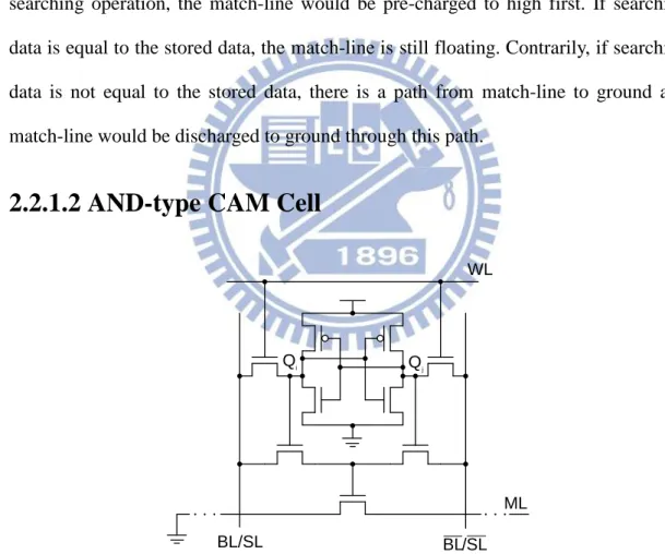
searching operation, the match-line would be pre-charged to high first. If searching
data is equal to the stored data, the match-line is still floating. Contrarily, if searching
data is not equal to the stored data, there is a path from match-line to ground and
match-line would be discharged to ground through this path.
2.2.1.2 AND-type CAM Cell
Fig. 2.7 AND-type 9-transistor binary CAM cell.
An AND-type CAM cell is similar to 9-transistor CAM cell whatever it works in
write or read operation. The only one difference from 9T CAM cell is the match-line
scheme. Fig. 2.7 depicts an AND-type CAM cell and Table 2.2 describes the truth
ML WL BL/SL BL/SL i Q j Q
table of AND-type CAM cell. As an AND-type CAM cell works in search operation,
the match-line would be pre-charged to high first. In contrary, the match-line hold
floating when the search data doesn’t match with stored data and the match-line is
discharged to ground only while the search data and stored data are match.
Table 2.2 Truth table of AND-type binary CAM cell.
State Qi SL ML
Zero (0) 0 0 0
0 1 floating
One (1) 1 0 floating
1 1 0
2.2.2 Ternary CAM Cell
For the CAM circuit design, the ternary CAM (TCAM) performs a more powerful
data search function [2.1]. Different from binary CAM which has two states: one (1) and zero (0) state, the ternary CAM (TCAM) cell has an additional state: don’t care (X) state. Alike binary CAM cell, TCAM would be classified into two kinds:
NOR-type TCAM cell and AND-type TCAM cell.
2.2.2.1 NOR-type TCAM Cell
Fig. 2.8 Static NOR-type ternary CAM cell.
SL DL/ DL ML j Q WL BL BL/SL i Q M1 M3 M2 M4
Table 2.3 State assignments and truth table for static TCAM cell. State Qi Qj SL ML Zero (0) 0 1 0 floating 0 1 1 0 One (1) 1 0 0 0 1 0 1 floating Don’t care (X) 0 0 0 floating 0 0 1 floating Not allowed 1 1 0 — 1 1 1 —
Fig. 2.8 shows a static NOR-type TCAM cell. It consists of 2-SRAM and
comparison circuits. This TCAM cell is designed to store three states, namely zero (0),
one (1) and don’ care (X). These three states are set by Qi and Qj. Table 2.3 illustrates how the three states are stored in this TCAM cell and the truth table of the static
NOR-type TCAM cell. When Qi is low and Qj is high, the TCAM cell is in the “zero”
state. In the searching operation, the same as BCAM cell, match-line will be charged
to high first. If search data is low, the NMOS M1 and M4 would not be turned on,
such that the ML will still be floating. On the other hand, while search data is high,
the NMOS M1 and M2 are turned on at the same time result in the match-line being
discharged to ground. However, the TCAM cell is in the “one” state, while search data
is high, the match-line would keep high. While search data is low, the match-line
would be discharge to the ground. Particularly, while Qi and Qj are both low, the
TCAM cell is in “don’t care” state. No matter search data is high or is low, the NMOS
M1 and M3 are not turned on result in the match-line keeping floating. Note that Qi
and Qj cannot be high simultaneously, this state are not be allowed.
There is an additional dynamic NOR-type TCAM cell is called dynamic TCAM
cell and dynamic TCAM cell is that the storage memories composed of 2 SRAM cells
in static TCAM cell are replaced by 2 capacitances in dynamic TCAM cell. The
dynamic TCAM cell works like static TCAM and Table 2.3 also shows how these
three states are stored in this dynamic TCAM cell and the truth table of the dynamic
TCAM cell.
Fig. 2.9 Dynamic NOR-type ternary CAM cell.
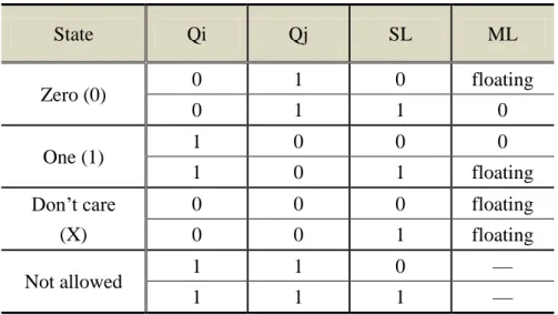
2.2.2.2 AND-type TCAM Cell
Fig. 2.10 AND-type ternary CAM cell. j Q i Q /SL BL SL BL/ ML WL WL BL/SL BL/SL DL DL ML Qi Qj
Table 2.4 State assignments for TCAM cell. State Qi Qj SL ML Zero (0) 0 0 0 0 0 0 1 floating One (1) 1 0 0 floating 1 0 1 0 Don’t Care (X) 0 1 0 0 0 1 1 0 1 1 0 0 1 1 1 0
Fig. 2.10 illustrates a 16-transistor AND-type TCAM cell which includes
2-SRAM and comparison circuits composed of three NMOS. The state assignments
and truth table of this TCAM cell is described in Table 2.4. The AND-type TCAM cell
is alike a 9-transistor AND-type BCAM cell when TCAM cell works in zero (0) and
one (1) states. However, while this AND-type TCAM cell is in don’t care (X) state
(Qj is high), no matter the search data is high or low, the match-line would be
discharged.
2.3 Low Power Match-line Schemes
The dynamic power consumed by a single match-line that misses is due to the
rising edge during pre-charge and the falling edge during evaluation, and is given by
the equation, Eq. (2.1), where f is the frequency of search operations. In the case of a
match, the power consumption associated with a single match-line depends on the
previous state of the match-line. Typically, there is only a small number of matching
we can neglect this power consumption. Accordingly, the overall match-line power
consumption of a CAM block with w match-lines is derived in Eq. (2.2).
𝑃𝑀𝐿 = 𝑤 ∙ 𝑃𝑚𝑖𝑠𝑠= 𝑤 ∙ 𝐶𝑀𝐿∙ 𝑉𝐷𝐷2∙ 𝑓 (2.2) With the advance of technology, noises are increasing the soft-error rate of
dynamic circuitries. Therefore, a low power, high speed and noise-tolerant TCAM is
expected. There has been large variety of techniques to reduce the power consumption
of match lines which are categorized as follow.
2.3.1 Conventional Match-line Structure
In the conventional CAM architecture, the circuit design of CAM word circuits
adopts dynamic CMOS circuits to improve data matching performance and hardware
cost. Applying the dynamic CMOS circuits designs, the conventional NOR-type CAM
word schemes and AND-type match-line schemes are shown in Fig. 2.11 and Fig.
2.12, respectively [2.27], [2.28].
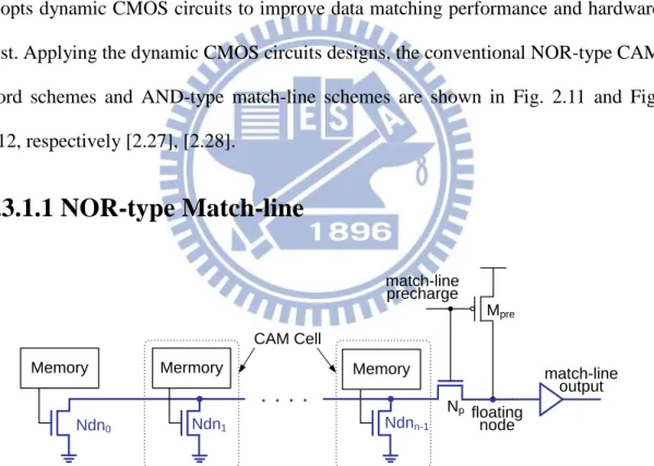
2.3.1.1 NOR-type Match-line
Memory Mermory Memory floating node match-line output match-line precharge Ndn1 Ndnn-1 Ndn0 Np CAM Cell MpreFig. 2.11 Structure of conventional NOR-type match-line.
Fig. 2.11 depicts, in schematic form, how NOR-type cells are connected in
parallel to form a NOR-type match-line. While we show CAM cells in the figure, the
description of match-line operation applies to both CAM and TCAM. A typical NOR
and match-line evaluation. First, the search-lines are discharged to disconnect the
match-lines from ground by disabling the pull down paths in each CAM cell. Second,
with the pull down paths disconnected, match-lines are pre-charges by Mpre. Finally,
the search-lines are driven to the search values, triggering the match-line evaluation
phase. In the case of a match, the ML voltage stays high as there is no discharging
path to ground. In the case of a miss, there is at least one path to ground that
discharges the ML. The match-line sense amplifier senses the voltage on ML, and
generates a corresponding full-rail search result. The main feature of the NOR-type
match-line is its high speed of operation. In the slowest case of a one-bit miss in a
word, the critical evaluation path is through the two series transistors in the cell that
form the pull down path. Even in this worst case, NOR-type evaluation is faster than
the NAND-type, where between 8 and 16 transistors form the evaluation path.
2.3.1.2 AND-type Match-line
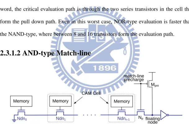
Memory Memory Memory floating node match-line precharge Ndnn-1 Ndn1 Ndn0 Np CAM Cell MpreFig. 2.12 Structure of conventional AND-type match-line.
Fig. 2.12 shows the structure of the AND-type match-line. A number of AND
CAM cells are cascaded to form the ML (this is, in fact, a floating node, but for
consistency we will refer to it as ML). On the right of the figure, the pre-charge
PMOS transistor, Mpre sets the initial voltage of the ML to the supply voltage. Then,
transistors are active, effectively creating a path to ground from the ML, hence
discharging ML to ground. In the case of a mismatch, at least one of the series NMOS
transistors is off, leaving the ML voltage high. The AND match-line has an explicit
evaluation transistor, Np, unlike the NOR match-line, where the CAM cells
themselves perform the evaluation.
There is a potential charge-sharing problem in the AND-type match-line. Charge
sharing occurs between the ML and the intermediate nodes. Referring to Fig. 2.12, if
all bits match except for the leftmost bit, there is charge sharing between the ML and
nodes Ndnn-1 through Ndn1 during evaluation. This charge sharing may cause the ML
voltage to drop sufficiently low such that the output inverter detects a false match. A
technique that eliminates charge sharing is to pre-charge high, in addition to ML, the
intermediate match nodes. This procedure eliminates charge sharing, since the
intermediate match nodes and the ML node are initially shorted. However, there is an
increase in the power consumption. Two drawbacks of the AND match-line are a
quadratic delay dependence on the number of cells, and a low noise margin.
2.3.2 Selective Pre-charge Scheme
Selective pre-charge, performs a match operation on the first few bits of a word
before activating the search of the remaining bits. As shown in Fig. 2.13, the CAM
word structure separates the searching operation into two comparison processes.
Partial bits among n bits data length are selected to perform the first comparison
process. If these partial bits of the input data mismatch those of a stored data, then the
input data mismatches the stored data [2.29]. Therefore, only very few word
Control SEG_2 SEG_1
Fig. 2.13 Word structure of the selective pre-charge scheme.
In the Selective pre-charge scheme, two different kinds of CAM cells are utilized
in the two segments respectively. In the SEG_1, the CAM cell is implemented as
XNOR-type and their pull-down transistors are arranged in the NAND type. The
NAND-type block is connected to the ground only when all the CAM cells of SEG_1
are matched. In contrast to SEG_1, we use the XOR-type CAM cell to implement the
SEG_2, and their pull-down transistors are placed in the NOR type. The NOR-type
block is disconnected from the ground only when all the CAM cells of SEG_2 are
matched [2.30]. Perhaps, selective pre-charge is the most common method used to
save power on match-lines [2.31]-[2.33], since it is both simple to implement and can
reduce power by a large amount in many CAM applications.
2.3.3 Pipelined Hierarchical Search Scheme
In selective pre-charge, the match-line is divided into two segments. More
generally, an implementation may divide the match-line into any number of segments,
where a match in a given segment results in a search operation in the next segment but
match-line segments in a pipelined fashion is the pipelined match-lines scheme
[2.34]-[2.37]. Fig. 2.14 shows the pipelined match-line, but with the match-line
broken into four match-line segments that are serially evaluated. If any stage misses,
the subsequent stages are shut off, resulting in power saving. The drawbacks of this
scheme are the increased latency and the area overhead due to the pipeline stages. By
itself, a pipelined match-line scheme is not as compelling as basic selective pre-charge;
however, pipelining enables the use of hierarchical search-lines, thus saving power.
C
C
C
C
x36 x36 x36 x36
enable
4 pipeline stages
match-line segment pipeline flop
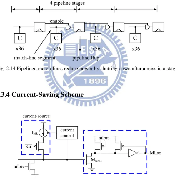
Fig. 2.14 Pipelined match-lines reduce power by shutting down after a miss in a stage
2.3.4 Current-Saving Scheme
mlpre Msense mlpre en IML current-source MLso current controlFig. 2.15 Current-saving match-line sensing scheme
sensing scheme which is a modified form of the current-race sensing scheme. The key
improvement of the current-saving scheme is to allocate a different amount of current
for a match than for a miss. In the current-saving scheme, matches are allocated a
larger current and misses are allocated a lower current. Since almost every match-line
has a miss, overall the scheme saves power. Fig. 2.15 shows a simplified schematic of
the current-saving scheme. This block is the mechanism by which a different amount
of current is allocated, based on a match or a miss. The input to this current-control
block is the match-line voltage, VML, and the output is a control voltage that
determines the current, IML, which charges the match-line. The current-control block
provides positive feedback since higher VML results in higher IML, which, in turn,
results in higher VML. In this scheme, the match-line is pre-charged low. The amount
of current is initially the same for all match-lines, but the current control reduces the
current provided to match-lines that miss (have a resistance to ground), but maintains
the current to match-lines that match (with no resistance to ground). The
current-control block increases the current as the voltage on the ML rises and the
voltage on the ML rises faster for large ML resistance. Since the amount of current
decreases with the number of misses, it follows that the power dissipated on the
match-line also depends on the number of bits that miss.
2.3.5 Wide-AND Match-line Scheme
A pipelined hierarchical search scheme improves search throughput, but results in
high area cost and large power consumed by flip-flops and clock drivers. Fig. 2.16
illustrates the 64-bit dynamic AND ML technique in each bank, which is designed
with four 16-bit wide dynamic AND gates connected sequentially. Only the first 16
triggered by the outputs of the preceding gates (clk1~clk3). The 16 bits wide AND
ML circuit consists of two 8 bits wide footed domino NOR gate local ML (lml0, lml1).
A footed domino is implemented to gate the evaluation of the next 16 bits wide AND
ML. This also enables a static circuit implementation of SLs, saving significant SL
switching power. The inherent logic function in each wide AND ML is a 16-bit NOR,
which is complemented through a clock gated NAND followed by an inverter,
deriving a fast domino compatible 16-bit wide AND function. This eliminates the
wide AND paths and realizes the complete critical path with 8-way dynamic OR
circuits. Therefore, the wide AND ML technique enables NOR-type CAM
performance with AND-type CAM power [2.45].
Fig. 2.16 64 bits sequential AND plan with swapped XOR cell and HS-AND match
circuit.
2.3.6 Tree Style AND-type Match-line Scheme
For original m-stage PF-CDPD AND-type match-line circuit, if the comparisons
to enable second stage comparison operation. Moreover, the match-lines divided into
many segments causes the size of comparison transistors being unnecessary too large
in the same search time criteria. Nevertheless, the speed enhancement comes at a cost.
To further speed-up of the PF-CDPD scheme, three versions of tree-style match lines
are shown in Fig. 2.17. Fig. 2.17 (a) uses two short parallel MLs in each half plane
and merges the output from both planes into a 4-input AND gate to generate the final
matching results. On the other hand, the design in Fig. 2.17 (b) and (c) use an 8-input
and 4-input AND gate, respectively, to generate the final matching results. The
designs of parallel, 3-level tree and 2-level tree have nearly 30% improvement on
search speed compared to original cascaded. However, compared to 233.6μW of
power consumption of the cascaded design, the parallel design and the 3-level tree
design have about 20% more power consumption and the 2-level design has only 9%
more power consumption due to a slight more complex inter-connection [2.46],
[2.47].
2.4 Low Power Search-line Schemes
Eliminating the search-line pre-charge phase is the common method of saving
search-line power. It reduces the togging of the search-lines, thus reducing power.
There are still other cases which can reduce the search-line.
2.4.1 Hierarchical Search-line Scheme
The basic idea of hierarchical search-lines is to exploit the fact that few
match-lines survive the first segment of the pipelined match-lines. With the
conventional search-line approach, even though only a small number of match-lines
survive the first segment, all search-lines are still driven. Instead of this, the
hierarchical search-line scheme divides the search-lines into a two-level hierarchy of
global search-lines (GSLs) and local search-lines (LSLs) [2.24]-[2.25],[2.48]-[2.51].
Fig. 2.18 shows a simplified hierarchical search-line scheme. In the figure, each LSL
feeds only a single match-line (for simplicity), but the number of match-lines per LSL
can be 64 to 256. The GSLs are active every cycle, but the LSLs are active only when
necessary. Activating LSLs is necessary when at least one of the match-lines fed by
the LSL is active. In many cases, an LSL will have no active match-lines in a given
cycle, hence there is no need to activate the LSL, saving power. The overall power
consumption on the search-lines is derived in Eq. (2.6), where α is the activity rate
of the LSLs. CGSL primarily consists of wiring capacitance, whereas CLSL consists of
wiring capacitance and the gate capacitance of the SL inputs of the CAM cells. The
factorα, which can be as low as 25% in some cases, is determined by the search data
and the data stored in the CAM. We see from Eq. (2.6) that determines how much
GSLs. Thus, the power dissipated by the GSLs must be sufficiently small so that
overall search-line power is lower than that using the conventional approach.
𝑃𝑆𝐿 = (𝐶𝐺𝑆𝐿∙ 𝑉𝐷𝐷2+ 𝛼 ∙ 𝐶𝐿𝑆𝐿∙ 𝑉𝐷𝐷2) ∙ 𝑓 (2.6) 𝑃𝑆𝐿 = 2𝑛 ∙ (𝐶𝐺𝑆𝐿∙ 𝑉𝐿𝑂𝑊2+ 𝛼 ∙ 𝐶𝐿𝑆𝐿∙ 𝑉𝐷𝐷2) ∙ 𝑓 (2.7) If wiring capacitance is small compared to the parasitic transistor capacitance
[2.49], then the scheme saves power. However, as transistor dimensions scale down, it
is expected that wiring capacitance will increase relative to transistor parasitic
capacitance. In the situation where wiring capacitance is comparable or larger than the
parasitic transistor capacitance, CGSL and CLSL will be similar in size, resulting in no
power savings. In this case, small-swing signaling on the GSLs can reduce the power
of the GSLs compared to that of the full-swing LSLs. This power equation of the
modified search-line scheme is derived in Eq. (2.7). This scheme requires an amplifier
to convert the low-swing GSL signal to the full-swing signals on the LSLs.
Fortunately, there is only a small number of these amplifiers per search-line, so that
the area and power overhead of this extra circuitry is small.
2.4.2 Charge-Recycling Search-line Driver
The SLs consume power only when the search data change, In general, the
transition probability of SL is smaller than one half. The non-pre-charged SLs
consume less power than half of that of the pre-charged SLs [2.52]. The driver further
saves the SL power be recycling the charge of SLs. Fig. 2.19 shows the
Charge-Recycling Search-Line Driver (CRSLD) architecture. Initially, the SLCR is
“0”. The transistor P1 turns on. The CR is “0”. The transmission gates T1 and T2 turn off. Two tri-state drivers D1 and D2 drive the SL pairs. The latch holds the data of
SLs. The SLCR becomes “1”. The transistor N1 turns on. When the search data
change from “0” to “1”, the transistors, N2 and N3, turn on. Then the search data
change from “1” to “0”, the transistors, N4 and N5, turn on. Therefore, the CR
becomes “1”. T1 turns on and two SLs share their charges. The SLs become VDD/2.
T2 turns on and the latch updates its data. If the search data don not change, the CR
remains at “0”. The SLCR returns to “0” and the CR becomes “0”. T1 and T2 turn off.
D1 and D2 drive the SL pairs from VDD/2 to VDD or ground [2.53]. Without the loss of
the memory utilization, the CRSLD reduces the SL power by recycling the charge of
SLs without the SL pre-charge.
2.4.3 Two-Level Don’t-Care Gating Scheme
The two-level DCG scheme exploits the vertically continuous “don’t-care” feature
[2.54]. Therefore, to gate the search data from being broadcast over the entire SL, this
design inserts the gating nodes to break the entire SL into several segments. As shown
in Fig. 2.20 (a), the level-1 (L1) gating node (GNL1) is implemented as an inverter that
is controlled by the corresponding mask bit. For example, a GNL1 is located in the ith
cell. When the ith cell is “X”, Mi=1 will cut off both the power and ground sources to
disable the inverter from transmitting the search data.
Fig. 2.20 (a) L1 gating node (GNL1) implementation. (b) L2 DCG example.
The L1 DCG is beneficial to reduce the SL power only when the first TCAM cell
is “X” in a segment. If the first cell is not “X”, this segment would be driven to perform the search operation even though the remainder cells are all “X”. To improve the power efficiency of the L1 DCG, the level-2 (L2) gating scheme to further exploit
the vertically continuous “X” property within an L1 segment. Fig. 2.20 (b) shows an L2 gating example, in which the L2 granularity (GL2) is 4. Similar to GNL1, the
function of the L2 gating node (GNL2) is to either gate or transmit the search data
2.20 (b), which is controlled by the mask value of the first cell (M0) in the
corresponding L2 segment. Thus, all side effects incurred by the floating Q and Qb
nodes can completely be eliminated.
2.4.4 Low Swing Search-line Scheme
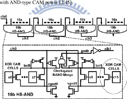
Fig. 2.21 Operation of a NOR-cell in the LSSL-CAM. (a) Mismatch. (b) Match.
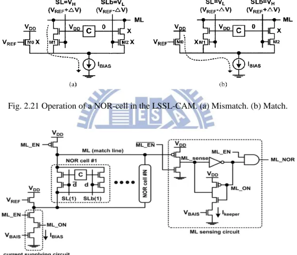
Fig. 2.22 Schematic of the NOR-cell block in the LSSL_CAM.
By comparing stored data with the low swing search data on the search-lines, a
low power CAM using low swing search-lines is presented. Fig. 2.21 shows the
operation of a NOR-cell in the low swing search line (LSSL) CAM [2.55]. In order to
compare the stored data with the low swing search data on a SL pair, M0 and a bias
mismatch case, the voltages of SL and SLb are VH (=VREF+∆V) and VL (=VREF-∆V),
respectively. The gate voltage of M1 is ∆V higher than that of M0. Therefore, IBIAS
flows through M1. The ML is thereby discharged to ground. In a match case, IBIAS
flows through M0 and the ML remains at VDD. Thus, the SL swing voltage
(∆VSL=2x∆V) in the LSSL-CAM is much smaller than the full swing voltage in the
conventional CAMs.
Fig. 2.22 shows the schematic of the NOR-cell block in the LSSL-CAM. In order
to reduce the ML power consumption, IBIAS is dynamically controlled by the ML_EN
and ML_ON signals. Initially, the ML_ON signal is set to the logic “1”. After the SL voltages change, the ML_EN signal is set to “1”. This enables IBIAS to flow. If all the
NOR-cells are matched, the ML remains at VDD. If not, the IBIAS flowing through the
mismatched NOR-cells decreases the ML voltage. The IBIAS control scheme reduces
the power consumption in all of the mismatched MLs by limiting the ∆VML. Only a
matched ML consumes the IBIAS until the ML_EN signal returns to “0”.
2.5 Low Power Design Techniques for CAM/TCAM
Macro
2.5.1 Power-Gated ML Sensing
Due to parallel match-line comparison, CAM is power-hungry. Thus, robust, high
speed and low power ML sense amplifiers are highly sought-after in CAM designs.
An effective gated-power technique of ML sensing reduces the peak and average
power consumption and enhances the robustness of the design against process
variations [2.32], [2.33]. The new CAM architecture and the row-based ML sense
as the conventional NOR CAM and use a similar ML structure. However, the
comparison unit and the SRAM unit are powered by two separate metal rails, namely
VDDML and the VDDC, respectively. The VDDML is independently controlled by a power
transistor (Px) and a feedback loop that can auto turn off the ML current to save power.
The separated power rails of VDD and VDDML is to completely isolate the SRAM cell
from any possibility of power disturbances during compare cycle.
Fig. 2.23 Row-based ML sense amplifier and new CAM architecture.
As shown in Fig. 2.23, the gated-power transistor Px, is controlled by a feedback
loop, denoted as “Power Control” which will automatically turn off Px once the voltage on the ML reaches a certain threshold. At the beginning the ML is first
initialized by a global control signal EN. At this time, signal EN is set to low and the
power transistor Px is turned OFF. After that, signal EN turns HIGH and initiates the
compare phase. If one or more mismatches happen in the CAM cells, the ML will be
charged up. When the voltage of the ML reaches the threshold voltage of M8, voltage
at node C1 will be toggled and thus the power transistor Px is turned off again. As the
result, the ML is not fully charged to VDD, but limited to some voltage slightly above
2.5.2 Self-Disable Sensing Technique
In order to resolve the design dilemma of the prior NOR-type and NAND-type
CAMs described in Section 2.2, a differential NAND-type CAM is presented in Fig.
2.24. Notably, MSi is turned on only if BL<i> and Q are logically opposite. That is,
SML<i> will be charged by ML<i> when the search key is opposite to the
corresponding bit of the word. The voltage drop between ML<i> and SML<i> will be
sensed by the differential MLSA (DMLSA). The speed of the comparison will be
fastened by parallel charging paths. Most important of all, the dc grounding path is
removed to reduce the static power consumption [2.56].
Fig. 2.24 The differential NAND CAM cell. The block M and block DMLSA denote a
memory cell to store the data bit and differential ML sense amplifier
The detailed schematic of the DMLSA for differential NAND-type CAM is shown
in Fig. 2.25. The DMLSA senses the voltage on the ML<i> and SML<i> to tell if the
word is “match” or “mismatch,” and then automatically disables the charge path to save the power. Notably, a signal will set the DMLSA into an initial state, where
DMLSA in the searching process is described as follow.
Fig. 2.25 DMLSA.
1) “Mismatch”: SEARCH = SEARCH_EN is pulled to high at the beginning of the searching process. Then, MN1 is turned on to charge the ML<i> such that KP will
be discharged but not totally pulled down to 0. If there is any “mismatch” CAM cell, MSi is turned on to make a current path between ML<i> and SML<i>. When the
voltage of SML<i> is high enough to turn off MP3, the voltage of KP will be pulled
down such that MATCHB is equal to logic 1 (mismatch). By two feedback paths,
MATCHB turns MN3 on and MP1 off, respectively, such that the current path of MP1
is shut off to choke the charge current of ML<i>. Therefore, the power consumption is
reduced after the searching process.
2) “Match”: If all of the CAM cells are “match,” ML<i> and SML<i> are isolated without any current path. The voltage difference between ML<i> and SML<i> creates
an output current of the differential pair (MP2 and MP3) to charge the KP and SP. As
soon as KP is charged to high, MATCHB becomes logic 0 (match). After the SP is
raised to high, SEARCH will equal to logic 0 and turn off MN1 to choke the charge
current to ML<i>.
comparison has been decided, regardless what the result is. By using the choking
current method to reduce the unnecessary dc currents, the power consumption is
significantly reduced. Moreover, the comparison process has been accelerated by a
positive loop to reduce the unwanted power dissipation.
2.5.3 Dynamic Power Source (DPS) Technique
Fig. 2.26 DPS technique. (a) DPSVDD implementation. (b) DPSGND
implementation.
Leakage-suppressed designs can be grouped into state-preserved [2.57] and
state-destructive strategies. The prefix data are unnecessary in determining the match
result in case of “X”, this technique uses the state-destructive strategy to reduce the leakage power dissipated in the “X” TCAM cells [2.58].
Similar to the traditional power-gated technique, there are two implementations
for the DPS design. Fig. 2.26 (a) first shows the DPSVDD implementation, where the
sources of P1 and P2 are connected to the Mb node of the mask SRAM. If the TCAM
cell is “X”, then Mb is 0, which will lower the D voltage to destroy the stored prefix data. In order to improve DPSVDD, Fig. 2.26 (b) shows the DPSGND implementation
cell is “X”, then M=1 will raise the voltage of Db to destroy the stored prefix data. Otherwise, M=0 will retain the stored prefix data in the “care” state. For an “X” TCAM cell, DPSGND has roughly 58% reduction that is the best among all possible
implementations.
2.5.4 Variability-Tolerance CAM Cells with NOR-type
Match-lines
Fig. 2.27 (a) NVT-BCAM cell with NOR-type match-line. (b) Read/Write timing
sequence of the NVT-BCAM cell.
Within-chip variability has become a serious problem in modern nano-scale
technologies, which is particular true for semiconductor memory designs. The
variability-tolerant BCAM cell is designed by separating the read port from the write
port such that the sizing for read static noise margin and write trip voltage is
decoupled [2.59]. Fig. 2.27 (a) shows the N-type variability-tolerant BCAM
(NVT-BCAM) cell with an NOR-type match-line. An MN4 is added in the comparator
for performing the read operation. Fig. 2.27 (b) shows the timing sequence of the read
and write operation of the NVT-BCAM cell. Consider that the NVT-BCAM cell