wtierc I$/(,) is tlie autocorielation functioii of thc Ilh path, iiiitl p k and .EA denote tlic lime position and limsmittcd eiiergy assuciiiletl
with Ihc kth syinbul, respcctivcly. As caii he obscrvctl Trotn q l i , 5, the lihlCE reccivcr iiiust 1i;ivc knowledge or tlic ctianncl (such as UPS, Bo and M[P) (ogethcr wilh that of 17i so that it ciiii
construct V!
to
ohtaiii \he vectors { I L ).
Since iioiic of Ihesc paramclerr are knuwn preciscly by the rcccivcr, wc itdopl an :ipproximation ofF,
i n tlie furni given Iiy cqii.5
mil iiicrchc miapproximation of [lie vectors 1. l,Wl /-U,kJJ ' 0 io 1 10 [r w m .2 10 3
To estimate the
MAP
channel, w c tise (lie MAP criterion lo obkiin an estirn;itc or {C,)$! by mnairnisiiig [lie (8 po.rtwiori mi- dilioiid T'DFp({G,]Gl { R d j i )
with rcspccr tn {G,j;$, D i r e c t l y solving this uptimisation problem is inlractohlc. 1 luwever, ii solu- lion ciin bc obtained casily using the ilerntivc LM dgorithm[?I.
Followiiig the proof outlined in [I], \ye c;iti write the mth coinpo- lien1 or tlic re-csliiiiiite
Gkll
I ) a~ (he clth ilcr;iLiou aswhere
H,,,,,
is thc kth component of the vectorN,,,,
aiitl SA is ihc: alphabct set takcii by Ai. As ci111 beseen
in c t p . 6, wc dso need to know lo 10 coinpilie C,(r/klb.TIE irerntivc sciiddiiid MAP CEA is carried out ti fixcd number of times I). The chaiiiiel estimate ohlainctl at llic last itcr- ation is usctl for inaximd ratio conibiiiiiig t h t provides tlic s o n
outputs [ I , 21. Assiiming iincotlcd binary phase shift keying (DPSK), syritbol ilccodiiig is 1xKlrFornied by I i a ~ l dccision oii tlic
rcal pdrt of AA(").
ELECTRONlCS LHTEERS
16th March
2000
Vol. 36
To propcrly cxecute llic 1:M algorithm sleps, thc R A K E
rcaiver stioiild possess av;iil;tble cstiinatcs u f tlic Dopplcr spread U,), the Iioisc: variarm 10, (Iic avc.rage PUWUS @,
(0)
of ill1 corisid-el ed pailis niitl the tr;insiiiittetl symbol cncrgiew hk,
S h z d ~ t t i t w resirlts wd U O I I C I W ~ ~ ~ : We restrict our treiilnient to a IjMTSNDIl uplink low-rile data scrvicc in the vehicular cnvirow
merit 141 where tlie pilol syinhols iirc sprcitl,
and
a11 tht. symbolsi i r c Iransinitted with ctlunl energy EA = hi, V k . Thc chaiiiicl niurlcl
is ILU vehicular A
[5]
and tlic niimber of RAKE fingers is choseira s tlircc. For our cwlutltion, w e considered two vehicular sped values Y = 120kmdl1, 500ktll/h, Tuiii. 1</4, vahics - 4 , 0, 4 a i d 8dB, icr rrcqucncy
Jk
= 192CiHz. Thc simiilaiions ~vcir' car- rictl O N withD
=5
iterations. We wssuiricd h t ilie shapc ol' the l)l'S was known by the rcccivcr but that thc xvcrtige powcrs ofrhcpallls wcrc unknown. Thc rmiver tlicrcforc ;)clopted ii unil'olni MIP \vhcrc ill1 p>~tli powcrs were taken to bc cqual, i.e. Q,(O) = I/
I>,
v
1.Figs. I ~ 3 rlisphy the sensitivity of lhe CEA with respect to iiii
cstiiuated encrgy in jj,), L; and respectivcly, r:or Y = I~IJ!",
the curves arc almost Iht, intlicaliiig that for low tn morleratc
I lopplcr sprciiding, the MAP Ct<A is robusl lo paiaiiictcr cstima- tion crrors. For v
--
500kiii/li, thc cffccls of e m " ~x~ranickrsilrc visiblc jii thc high E/lh reginn, wliereaq the loiv E/J" rcgioii cxhibih greater robustness. Of the three pwiizetcrs coiiceriictl, [lie M A P CFA is niosl wisilivc to It,). Neverthclcss, the scrisilivity
with respect to this p,iramctcr is visible only i i i thc high Doppler C H S C , bcing inore proiioiiiiceil in thc high l?lo i-cgion.
I n cunclurinn, thc rcsiilts sliow thai tlic semi-blind MAP CEA IS rcl;ttivc.ly robust to crrors in estimaliiig
&,
E, io, i i n d crwi bc usedcvcn jib cliniiiicls with s w c r e Dopplcr s p r e d n g .
Itcfcrccmcs
Power PHEMT
with compact
device
layout
for
low
voltage
CDMA
application
E.Y.
Chnrig, Ui-Hourig Lee, S.11.
Clien:~nd
H.C.Chang
A hiph cficiciicy low voltage upvralioii rlu;il deliti-dopcd AICi;iRd
InGaAs/GaAs ~xci1do11101-phic high dcclroii iiiobilily Ininsistor
(I'IIDMT) 1'oi loiv votkigc codc division nioliiplc awcss (CtIMA)
q i p I i ~ h > i ~ h:ig b ~ i i dcvclopctl. Wlicn lcsicd at 2.4V t i n d t.')Olfi
rindci~ IS45 CDMA tiiorluletian, tlrc 20.16mm L'HI!MT dcvicc
was found 10 Iwc a l i n a i r uuiprrl lioiucr of 2Bdllin with a powcr
:idtlctl eKcicticy of 30.2% 'l'hc dcviw iilso IMS n siiliinitinti power
nl' 10.0dUiii with a powcr ~irlriecl cMicicncy ul' hl.Y!& The high
cfiicicncy iiiid 1inc:irily or Ilic I'IIEMT t t t low h i i s wlt:igc is iitrrihulcd tn ttic use 01' thc t l u d d d r a - c b p d P I I E M I struclurt and to the rctlucliori of thc s i x o l ~ l i c dcvicc Iiiyviil. ~l'hc dcviw: is suitihlc fur luw wltagc CDMA ,il>plications.
I n ~r~oriuciiun; Advmccd high perrorm R I ~ C C \vi rclcss coiiii nul 1 iaiti o n
systcms suclz iis digilal ccllulw pliotie aiitl swtcllilc comiunicatioii systcms require high efficiency power Lransislors opcratitig at w
low siipply voltage to iiicrcasc thc ialk time or the hiindsets.
rlevims for low voltage applinitions have bccn developed in rcccnt ycars [ I - 51. In this Lcllei-, i i c h i 1 delta-doped AIGaAs/liiGiiAs/ GwAs pseudomorphic high electron mobility transistor (PIIF.MT)
is presented which ciin he usecl i n low vollagc codc division multi- ple a ~ r c s s (CDMA) applicatioris. l'hc tlcvclopcd PHEMT also Iim
a very coinpist dcvicc layout. The r~xluction iii the device layout results iii a low kncc voltage aiitl low mircc resistance for Llic
device which iii;ikcs it suitable for IOW t>olkgc ;ipplicarions. Tlic dcvclopcd device 1w bwii cv:ilu;ttcd tor IS45 CDMA ;ipplica-
lions et 3.0 and
2.4V.
This Letter rcprcscrits the fii.st report of ii powerPH
EMT for 2.4V CDMA applic;rlions.AulGelN ilAu AuiG a/NilA U
30nm s i d o p i n g
i-GaAs 3.6nm
i-GaAs
AiGaAstGaAs superinnice
Device siwcizoa o / ~ d /uyoru: T h c device used in this Letter is ail AlCiaAs/[nGaAs/GsA\s b:iscd PHEMT. Thc epitaxial laycr was
grown hy R rnolccular bciirii cpitaxy (MBE) kcliniquc oii a 3iri (100) oriented seiIii-iiisiil~iliIi~ GiiAs wafer. Tlic structure of the
duiil dcltn-dopcd AiC;:iAs/[nl;;iAs/G,7As PHEMT i s shown in I;ig. I . Tlie capping laycr was doped to 5 x 10"/cm3 to foriii good
oliinic coniacts. I'hc two diinensiorlal elcclrori gas (2-DEG) wiis formed in the pseuclomorphic 11iC;iiAs clitiiiricl (lO0h) by clcctron tr'wlisfer rrom silicon delta doping abovc tind helow the InCaAs liiyer. Tlic GaAs spacer was grown bclwcen AIGiiAs mid IiiGaAs to iinprove thc intcrfiicc qunlily. Thc r;ihric;ttcd dcvice had n total p l c width o f 20.161~11~1 with c d i fingcr I20pn in lcngth. The drain to source spxiiig was +I mid the gnk leiigth 0.5pn. The rlcvicc had a n area I640 x 300pi2, which is quite c o i q ~ a c t coni- pared willi rcgiilirr power device I q o u l s .
Device jitbr.icnticirt: The dcvicc wiis processed usiiig ii skind;ird
power 1'1 I l.;MT process. Device isrilarioii WHS iiccomplislied by wct ctching using an W-basctl solutiori. Tlie ohmic mckil, Aii/Ge/Ni,
wiis dcpositcd by elcctiui-bc;im cwporatioii r o l l o ~ ~ d by rapid
tliermal anncaling iit 30O0C foi. 10s. Tlic doiible gale i " c s s wiis pcrfornied to iiicrcasc tlic dcvicc hresktlowii anti rcdiicc ihe ilevicc sourcc resishiiw using it dilute citric acid hiscd solution. The g;rlu lcngth OF the device was 0.5pnm, clcfiiml by tlecp U V lithography. The gate mclsl wiis fbrnicd by Llir clcctroii-beam cvaporiiliol-1 of
TilPllAu mctal. Pliisrna enharicetl chcmiciil vapour tleposilion (PECVD) silicon nilride was used for tlie tlcvicc pirssivation. Gold plated aihridges were uscd for ititcrcoiiiiectioiis. The plated gold Ihickncss wi19 -2.5~1117. After thc fiwtside w i i s coniplctcd, the device wiis thinncd to 5 i i i l and nicballiscd with plated gold on lhc
backsidc 10 impruvc tlic thermal dissiptiliun of tlic dcvice. &pice pc@v/trrict: Thc dcvelnpecl dcvicc liiis :I siituraliaii current
of hA. The piiicli-om voItagc of tlic devicc is around -1
, I
V, Thccontwt ixsistaticc I?,: of the dcvice willi 120pi gatc width is lO6111Q. The inaxinitam triinscoiidub;lnceict~it~~ nf this devim is 340 Ins/
mm.
'L'lic gate-to-drain hrcakdown voltagz delined ;it a gatc-to- drain currenr rlciisity of I InNrnni is I2V. ' l l i c high ciirrcnt density ;tnd tl'at~scoiid~ic~nncc of this device iirc duc to thednal
della-ilop~l PIIEMT structure.
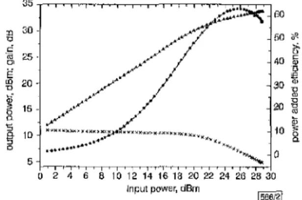
The pniver pcrfomancc of this 0.5 p i
x
ZO.llimm device wiis n i c i i s u r d at 1.9G1-I~ with drain biascs of 3.0 and 2.4V. Fig. 2shows the nutput powcr ;itid powcr added cficicncy against input
powcr Tor the 20. lhmrn wick &vice iit 3.0V drain bias. The tcsting
conditions wcrc as follows:
r$
= --0.9 I V,v,,
= 3.0V, idlc currcnt = 300mA. At 32,77dBin oldput power, the device has an cff- cieiicynr
63.04'/0, iiticl ihe gain nt this point is 7.12d13. Fig. 3 diows the powcr pcrforin;mcc of ihe 20. I bmin device when tcstcda t 2.4V. I'he dcvicc was o p x i t e d iindcr class AB conditions with
ii l i a s drain ciirrciit of 4001nA.
FOF
l h c 20.lhinm devicc, iindcr 2.4V hias coiidi(icms, the maximuin ontptit. power is 3fldBlil slid llic power i1dded clliciciiq of this device a l ~ h c niiiximiiiii outpi( power is OI.S',%. The gxiii or this dcvicc at tlic iixixiinuiii oiitput power is R.47rllI. Tlic lincar gain w i s II.SbclB and the oiilput powcr at 1 dn comprcssioii was 28.12dlhn with a power atldcrlcfkicncy of 47.5%).
'g
::I
L" 25.8
1 5 - 5 n I D D 5-
. . . 0 2 4 6 8 10 12 14 16 18 20 22 24 20 28 301606121
Input power, dBmFig. 2 /'i~iwr pcifoi'inirrioe qf 20. I l j i i r n z clcvico I{? 1.9GIrz ,frcqwtrcy w r h 3.0 V d t ~ i ! r ~ m r e c hiiis \wlmgi! ( i d 300inA i t l k clrniti w r i c n i
--C liower ~tiidcii cfficicricv
-Ap UUtI"11 powcl'
'L'hc dcvicc w a s also Lcstcd at I.9CiHz uiirlcr [S-95 CDMA motl-
ulalion. At 9.OV bias, tlic lesling condition foI thc CDMA modu-
latinii wm :is follows: V,, = . 0.91 V,
V,,
3.OV, irllc: cui-rciit =300niR. At 2R.02dBm output power, Ihc dcvice gsriii is Y.8ldl3, (lie puwcr iiddcd eflicieiicy is 37,X'5, aiitl l h e dcvicc has ail adja- ceiit chiiiiiicl power rejection [ACI'R) o f . 30.70dUc zit l . 2 5 M H ~
offset arid -.48.67dBc at 2,25MIIz otkct, as shown in ljg. 4. The dcvicc WRS nlso tcslctl at 2.4V unrlcr IS-95 CDMA moddatiori. Thc test pariunelcrs u w c a s tbllows: (,,, = -0.74V, V,!.% = 2.4V,
irllc ctirrcnt = XOOniA. At 2XdBm oulpul puwvcr, tlie device giin is i 1 .OSdlI, ;incl t h e devicc hiis ;I power added cfhicnc.y of 30.2%). Fig. 5 slio~vs ihc ACPR spcctrmn
Tor
the device under 2.4 V drain bias testing conditions. At 2 8 d h liuc;ir output powcr, tlic device has a n ACPR of-31.46dIk ;it 1.25MHz oTTsct iiiiil 4X.X3dBc a1578
ELECTRONKSLETTERS
16th
March 2000
Vol.36
No.6
2.25MH;r nffsci. 'I'he dcvclo~ctl dexiiw meets ihc IS-95 CUMA device spccilicwtions under hoth 3.0V and 2.4V biws contlitioiis.
CrirrcirrsWts; A low voltage p o i w PHEMI' tbr CDMA applicii- tions IiiiS heen dcvcloped. Thc device h;is it double delta-tioped AIG~IAS~GJIA~/CT:IAS s(ructii rc to providc high drain current dcnsity aiicl transcoiiductaiic. 'l'lie size of l l i e layout of [lie dcvicc was mduccd tn iinpruvc the low tlic vnltagc pcrkmxincc. A1 2.4V bias, Ihc dcvdopcd devicc show? an oulpul powcr or 36dHni with :I powcr added eificicricy nf bI.ST4 arid tlic gaiil of thc dcvice at
maximuin output powur i s 8.47dU. Wlicri icstctl under IS-95 CDMA ruodul;ilioii conditions, llic dcvicc iiwcts ilic CIJMA spw
ificiitions a1 huth 3.OV illid 2 . 4 V tlinin I h . A1 2 M B m lincar out- put pnwcr hiq CDMA ;ipplication, the devicc lltis ii powcr iitkled
eRlcicticy or 373%) ;it 3.0V hias and 30.2%~ a t 2.4V bias. This Ltt- tcr represenis thc first reporl 011 powcr I'lIEMTs for 2.4V CDMA spplications. The dcvicc slioiild bc iipplicahk 10 the ncxl genera- tion of digital wirelcss coininunic;itioii systems.