WE2C-2
Low
RF
loss and noise of transmission lines on Si substrates using
an improved ion implantation process
~K. T. Chana, Albert Chin",
S. P.
McAlisteP, C.
Y. Chang', C. Tsengd, V. Liangd, J. K. Chend,
S.
C.
Chiend, D.
S. Duhe, and
W. J. Line
aDept.
of
Electronics Eng., National Chiao Tung Univ., Hsinchu, Taiwan
bNational Research Council, Ottawa, Canada
Dept.
of
Communication Eng., National Chiao Tung Univ., Hsinchu, Taiwan
United Microelectronics Corp., Hsinchu, Taiwan
'Inst. of Nuclear Energy Research, Taoyuan, Taiwan,
d
Absfrucf
_-
Very low power loss i 0.6 dB at 110 GHz andnoise of c 0.25 dB at 18 GHz have been measured on transmission lines fabricated on Si substrates and implanted with proton. In contrast, much worse power loss of 5 dB and higher noise of 2.5 dB were measured without implantation.
This large improvement arises from the high resistivity by proton implantation, which was also done after forming the transmission lines and at a reduced energy of
-
4 MeV for easier process integration into current VLSI technology.I. INTRODUCTION
Owing to the rapid evolution of MOSFET technology, Si has been used for
RF
applications, because of the inherent excellent integration capability. However, the high substrate loss and cross-talk, due to the low resistivity of Si (-10 0-cm), have become some of the main technology challenges to realize high performance SiMMICs.
Even advanced SO1 technology shows little improvement in substrate loss and cross-talk because very thick isolation is necessary to block the microwave penetration for RF performance improvement. Recently, we have developed a simple ion implantation process[1]-[6] which can significantly increase the Si resistivity
from the standard IO 0 - c m to
-
lo6 0 - c m [I]. This high resistivity can be maintained at 400 "C and has little side-effect on masked gate-oxide integrity, even after being integrated into a VLSI back-end process. Excellent antennas and transmission lines up to 20 GHz have been demonstrated [5]. In this paper we show data on the RFnoise, at up to 18 GHz, and the RF loss, up to 110 GHz, of transmission lines fabricated on ion-implanted Si.
0-7803-7695-1/03/$17.00 0 2003 IEEE
Excellent RF noise of
<
0.25 dB to 18 GHz and very low power loss, 5 0.6 dB up to 110 GHz, have been measured on proton-implanted transmission lines on Si. This is much better than for transmission lines on oxide-isolated Si without the implantation. The modified implantation sequence, done after device fabrication, not only reduces the disruption to a VLSI process line but also extends the maximum possible operation frequency from 5 9 0 GHz to1100 GHz. Reducing the implantation energy to
-
4 MeV also makes the approach feasible for production, through the use of a simple thick photoresist.WZ
11. EXPERIMENTAL PROCEDURE
Standard 4-in Si wafers, with a resistivity of I O O-cm, were used in this study. An additional 1.5 pm thermal Si02 was grown to increase the substrate isolation. Ion implantation of protons, from an ion cyclotron, was done to reduce the substrate loss further. The ion implantation was performed either before, or after device fabrication. In
the former case the wafer would face a subsequent 400 "C
thermal cycle in the backend process.
For
manufacturing considerations, we have reduced the implantation energy from 15 MeV to-
4 MeV by using an additional energy absorber.To
study theRF
noise dependence on the substrates, coplanar transmission lines of 1000 pm length,30 pm width, and 4 pm thickness were fabricated using AI metal. Two-port S-parameters were measured
up
to 110GHz using an
HP
851OC network analyzer andde-embedded from dummy pads. The RF noise figure and associated gain were measured from 1 to 18 GHz using an
9 6 3
Am - N PSB Noise Parameter Extraction System.
To
study the maximum possible operation frequency, beyond the upper limit of the network analyzer, we used a femto-second laser to measure the response time [3].-2
111. RESULTS AND DISCUSSION
A.
RF
noiseFig. 1 shows the measured R F noise of transmission lines fabricated on 1.5-pm
SiOz
isolated Si substrates, with or without the different proton implantation processes. The standard Si gives a noise figure of 0.5-
2.5 dB/mm from 1 GHz to 18 GHz. This amount ofRF
noise is even larger than the noise from MOSFETs [7]-[8], and scaling down the VLSI technologyfrom
0.18 to 0.13 pm MOSFET has negligible noise improvement [7]. Thus, theRF noise from transmission line will contribute significant noise to MMICs. In contrast, the 10l6 cm~’ proton implanted Si has a much improved RF noise of 5 0.25 dB in the 1
-
18 GHz range. The excellent RF noise is consistent with the high associated gain as shown in Fig. 2. The negative associated gain is due tothe
transmission lines being passive devices. The proton-implanted Si, done at reduced-
4 MeV energy after the backend process, shows excellent low noise and high gain - comparable with the high-energy 15 MeV implant done before the backend process. This suggests that it could be used for process integration into current VLSI technology.+Hlgh=nergypmton implimtation More b s b n d pmosos
-.=-
Low.energy pmtOn implantation altsr backem2 -
-
m
I
are
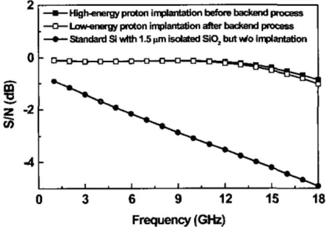
the highest, and the sequence of implantation has little effect. The worstS/N
ratio is shown by the standard Si with an S/N of -0.9- -5 dB/mm. This trend is the same asNF,;. and the associated gain. The SN ratio improvement
of
0.8
-
4.2
dB is frequency dependent indicating good potential for proton-implanted Si in R F applications, especially in the frequency range up t o 18 GHz.I
Q O
d
-1-
.-
C U a, m 0-
.-
g
-2a
v 0 3 6 9 12 15 18 F r e q ~ c y ( G WFig. 2. The frequency dependent associated gain for standard Si with 1.5-pm top isolation oxide, applied with or without the different proton implantation processes. The standard 1.5-pm SiOdSi without implantation shows very poor associated gain,
+ ~ ~ n g y p ” n i m p l a n t a t i m ~ ~ p a e e r
+-poton i i w 4 d m a f M k d m d
-
+standards( wlth 1 . 5 ~ isdded SiO, but d o implantation
0
!i
z
-23
4 0 3 6 9 12 15 18 Frequency (GHz)Fig. 3. S/N ratio of transmission lines fabricated on 1.5-pm
12 15 l8 SiOJSi substrates with or without the different proton implantation process. The S/N improves largely for transmission line with proton implantation, and the implantation sequence has little effect.
B .
RF
loss0
0 3 6 9
Frequency ( G W
Fig. 1. The measured RF NF- for standard Si with 1.5-pm top isolation oxide. aDolied with or without the different Droton .
..
implantation processes. The NF,,, of the standard Si increasesrapidly with increasing frequency. We have also measured the S-parameters of the
low-um long transmission lines UD to 110
GHz.
as shown ~ ~r~~~ ~ .~~~~~~~~ .~ ~ ~ ~ ~ L iTo
investigate the dependence of theRF
performance on the substrates, we compare the S/N ratio in Fig. 3.For
proton-implanted Si the S/N ratios of -0.1- -0.8 dB/mm
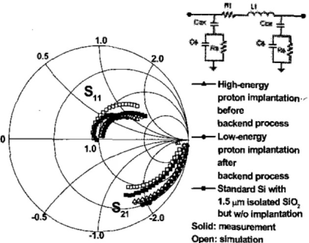
in Fig. 4. The lines are symmetrical
so
only S I , and S I , are shown. Both S I , show inductive behavior at the lower frequencies, starting at the center and spiraling clockwise. 964The additional loops may he due to resonances. The magnitude of transmission gain S21 on both the
proton-implanted Si stays relatively high over the whole frequency range, while the standard Si shows a smaller
ISztl. This result is consistent with the poor associated gain and S/N shown in Figs. 2 and 3.
With proton implantation -Without proton implantation
Fig. 4. The measured SI, and S21 of 1000-pm long transmission lines on the standard 1.5-pm SiOdSi substrates applied with or
without implantation. The magnitude of on the transmission line implanted with pmton is larger over the whole frequency
range than the same transmission line without implantation.
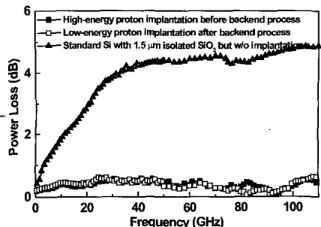
-4 .o
The power loss of the transmission lines, up to 110 GHz, is shown in Fig. 5. For those on 1.5 vm Si02-isolated standard Si, the loss increases monotonically with
increasing frequency - this is consistent with the
RF
associated gain shown in Fig. 2. The
-
5 dB higher powerloss, poorer RF noise, and much lower associated gain are some of the severe drawbacks of conventional Si RF
technology. In contrast, the 10l6 c m 2 proton-implanted Si provides improved power loss of
<
0.6 dB/mmup
to 110GHz and is close to the ideal case.
To
probe the maximum operation frequency beyond the upper limit of the network analyzer, we used a femto-second laser method [31. As shown in the Fig. 6,response times of
0.9
ps (1100 GHz) and 1.7 ps (590 GHz)were measured for implantation after and before device fabrication, respectively. These values are due to the high defect-density-related fast trap rate that gives high resistivity [3]. At high enough frequency, the trapped carriers can follow the signal and become active. The activated carriers at high frequencies will make the semi-insulating Si become conductive. The reduced maximum operation frequency, when the implantation was done before device fabrication,
is
due to the backend thermal cycle, which anneals out some of the defects.0 20 40
60
80 1000
FrsqNncy ( G W
Fig. 5 . Measured power loss of Umsmission lines on the standard 1.5-pm SiOdSi substrates up to 110 GHz, with and without the different proton implantation processes. The loss for the transmission line implanted with proton is much lower.
' 0 '
1~
Implantation after backend process .- Implantation before backend processLaser on
1500 3000 4500 6000 7500
Fig. 6 . Measured canier response by femto-second laser method. Response times for implantation after and before device fabrication is 0.9 ps (1100 GHz) and 1.7 ps (590 GHz), respectively.
C. Simulated Results
Time (fs)
In addition we have simulated the S-parameters to study
the dependence of the RF loss on different substrates. Fig.
7 shows the measured and simulated S-parameters, up to
18 GHz, for the transmission lines fabricated on variously treated Si substrates. The equivalent circuit schematic for the transmission line on Si with or without proton implantation appears in the insert. The S-parameters of the proton-implanted transmission lines
on
Si, applied before and after the backend process, are almost identical. The good agreement between the measured and modeled S-parameters suggests that the equivalent circuit model is appropriate. The extracted R, for the standard Si case is -350R,
much smaller than the 22500R
for the proton-implanted devices.proton implantation.-
backend pr-
pmon im@anta(ion
backend process 1.5 pm isolamd SiO,
but wlo implantatim
0 & Low.energy
+Standard Si with
solid ma*”m&
Open: simulation
Fig. 7. Simulated and measured S-parameters of transmission lines on Si substrates up to 18 GHz, applied with or without the different proton implantation processes. The inserted figure is the equivalent circuit model. Good agreement indicates that the model is appropriate.
Using the same model, we also calculated the
RF noise,
shown in Fig. 8. Good agreement between the measured and modeled noise is shown, assuming that the noise source is the thermal noise of the shunt
R,.
The relatively small substrate resistance for the standard Si increases the thermal noise of the transmission lines. The reason why the implantation process does not contribute to the excess noise in the 1 to 18 GHz range is due to the fast trapping time (high frequency) as shown in Fig. 6.+-H~pQani#+aItaionbefaeb&?mpocess ~ ~ ~ i n p l ~ m a f f e r b a e k e n l p m c e s s + ~ S w i t h l . 5 ~ 1 s d a t € d S 0 2 lMVr(0iyrm 0 0 3 6 9 12 15 18 Frequency ( G W
Fig. 8. Simulated and measured minimum noise figure of
transmission lines on Si substrates, applied with or without the different proton implantation processes. The noise source may result from the substrate shunt resisiance
K,
since a good fit is obtained.IV. CONCLUSIONS
We have achieved extremely low RF noise and power loss for transmission lines on proton-implanted Si that suggests potentially good process integration capability with; VLSI technology. The good isolation by proton implantation is directly related to the figure-of-merit of the RF performance for the Si transmission lines.
ACKNOWLEDGEMENT
We would like to thank D. C. Nio at National Chung-Shan Science Reseach Inst. for help with the RF
measurements. This work has been supported by NSC (90-22 15-E-009.044).
REFERENCES
[I] Y. H. Wu, A. Chm, K. H. Shih, C. C. Wu, S. C. Pai, C. C. Chi, and C. P. Liao, “RF loss and cross talk on extremely high resistivity (IOK-lMR-cm) Si fabricated by ion implantation,” IEEE M7T-S Int. Microwave Symp. Dig., pp. 221-224, June 2000.
[21 ,K. T. Chan, A. Chin, C. M. Kwei, D. T. Shien, and W. I. Lin,
“Transmission line Noise from Standard and Proton-Implanted Si,” IEEE M7T-S lnt. Microwave Symp. Dig., pp. 763.166, June 2001.
[31 A. Chin,
K.
Lee, B. C. Lin, and S. Homg, ”Picosecond photoresponse of carriers in Si ion-implanted Si,” Appl.Phys. Lett., vol. 69, pp. 653-655, 1996.
141 Y. H. Wu, A. Chin, K. H. Shih, C. C. Wu, C. P. Liao, S. C. Pai, C. C. Chi, “The fabrication of very high resistivity Si with low loss and cross talk,” IEEE Electron Device h i t . ,
vol. 21, no.9, pp. 442-444,2000.
[SI T. Chan, A. Chin, Y. B. Chan, T. S. Duh and W. J. Lin, “Integrated antenna on Si, proton-implanted Si and Si-onQuartz,” in Inc. Electron Devices Meetings (IEDM)
Tech. Dig., pp. 903-906, Dec. 2001.
[61 K.
T.
Chan, C. Y. Cheu, A. Chin, J. C. Hsieh, J. Liu, T. S.Duh, and W. J. Lin, “40-GHz Coplanar Waveguide Bandpass Filters on Silicon Substrate,” IEEE Wireless & Microwave Components Lett. 23, no. 11, pp. 429-431.2002.
[71 C. H. Huang, C. H. Lai, J. C. Hsieh and I. Liu and A. Chin, “RF noise in 0.18pm and 0.13pm MOSFETs,” IEEE
Wireless & Microwave Components Len. 23, no. 12, Dec.,
2002.
181 Y. H. Wu, A. Chin, C. S. Liang, and C. C. Wu, “The performance limiting factors as RF MOSFETs scaling down,” IEEE RF-IC Int. Microwave Symp. Dig., pp.
151-154, June 2000.