Journal of Engineering Technology and Education, ISSN 1813-3851
Analysis of photonic band gaps in two-dimensional Archimedean tiling
patterns
Jiun-Yeu Chen1, Jia-Yi Yeh2,*, Wei-Te Chen3
1R&D Planning Division, Office of Strategy and R&D Planning, ITRI, Hsinchu, Taiwan
2Department of Management Information Science, Chung Hwa University of Medical Technology, Tainan, Taiwan 3Department of Mechanical Engineering, National Cheng Kung University, Tainan, Taiwan
E-mail: [email protected]
Abstract
A theoretical discussion on the photonic band structures (PBSs) of two-dimensional Archimedean lattice photonic crystals (PhCs) is presented. The special focus is placed on the photonic band gaps in the Archimedean (32.4.3.4) and (4.82) lattices. The PBSs of the two lattices in the two cases of dielectric cylinders in air and air
circular holes in a dielectric material have shown similar photonic properties of basic Bravais lattice. In the case of dielectric cylinders in air, the (4.82) structure appears a similar property with the square lattice of air circular
columns drilled in a dielectric material. In the other case of air holes in a dielectric material, the (32.4.3.4) lattices
break the symmetry of lattice arrangement to open a complete band gap. The PhC structures presented in this article can provide a way for creating new photonic functional devices.
Keywords: Photonic crystals, Archimedean tiling, photonic quasi-crystals, photonic band gaps.
1. Introduction
In the last decades, the study of periodic dielectric structures has received considerable interest because it presents the ability to prevent the propagation of electromagnetic waves in a certain frequency range [1,2]. The theoretical study of photonic crystals (PhCs) in two dimensions (2Ds) is easier because of the fact that the wave propagation can be analyzed separately for two different polarizations; thus, the original vector problem is reduced to two scalar problems. These polarizations are transverse magnetic (TM) modes, if the electric field is perpendicular to the plane defining the structure, and transverse electric (TE) modes, if the same occurs for the magnetic field. When the band gaps for two different polarizations overlap, they create a combined band gap known as an absolute (full or complete) photonic band gap (PBG). Previous studies have focused on changing the shape of rods [3,4], reducing the symmetry of Bravais lattice [5], rotating noncircular rods [6-8], and adding interfacial layer [9,10] to create PBGs. Nevertheless, the band diagram of these lattices remains strongly dependent on the light propagation direction. Applications of these crystals in semiconductor lasers [11], solar cells [12], high-quality resonant cavities and filters [13] have also been proposed.
Archimedean tilings are periodic 2D structures with properties quite similar to those of photonic quasi-crystals (PQs). These tilings depicted by Kepler in Harmonices Mundi II are constructed from regular convex polygons of one or several types in plane patterns [14]. It is known that only eleven kinds of Archimedean tilings can fill the whole plane without gaps, including the traditional Bravais lattice [15]. In this article, a set of integers (n1.n2.n3…) denotes a tiling of a vertex type in the way that n1-gon, n2-gon, and n3-gon… meet consecutively on each vertex. For example, the symbol (4, 82) is the notation to categorize the Archimedean
lattices and means a tiling in which a square and two octangles gather edge-to-edge around a vertex.
Apart from periodic Archimedean lattices, PQs do not present any translational symmetry, but they exhibit rotational and mirror symmetry of unusual order. Recent studies have demonstrated that 2D complete PBGs can also exist in several quasi-periodic patterns such as fivefold, eightfold [16], and 12 fold [17]. To our knowledge, few authors have studied the arrangement effects on the photonic band structures of different Archimedean tilings. In this paper, the motivation for using Archimedean lattice PhCs is to find out the superiority and utility in PBGs based on their much higher degree of isotropy.
2. Model design and analysis
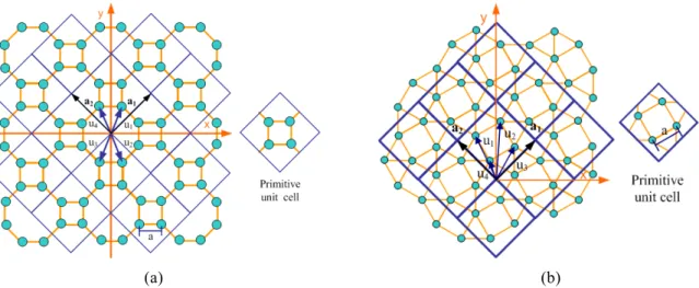
Like the super-cell concept used in calculating hexagonal photonic band structures [18], the positions of cylinders in the unit cell indicated by ui (i=1~4) are shown in Fig. 1, which presents the proposed 2D Archimedean
(4.82) and (32.4.3.4) PhCs constructed with primitive unit cells occupied by four cylinders. With the choice of the
coordinate axis in Fig. 1, the primitive cells of the structure are constructed from two primitive translation vectors a1=(1+1/ 2 )a(1,1) and a2=(1+1/ 2 )a(-1,1), where a is the lattice constant. The positions of the basic four pillars
with respect to the coordinate origin are u1, u2, u3 and u4 with u1=a(1/2, (1/2+1/ 2 )), u2=a(1/2,-(1/2+1/ 2 )),
u3=a(-1/2, -(1/2+1/ 2 )), and u4=a(-1/2, (1/2+1/ 2 )), respectively. This periodic structure can also regard as
clusters of four atoms organized in a square Bravais lattice, i.e., a modification version of the square lattice. It indicates that Wigner-Seitz cells can be defined and all the theoretical and numerical methods already known can be applied. For any integers l1,2, R=l1a1+l2a2 defines the Bravais lattice with the periodic dielectric constants
ε(r+R)= ε(r), where r is the position vector. The difference between (4.82) and (32.4.3.4) lattices is that the later
structure is the four cylinders arranged in a square rotated by 15° with respect to the square unit cell. With the choice of the coordinate axis in Fig. 1(b), the positions of the four cylinders are defined as u1= a(-0.683, 1.5416),
u2= a(0.183, 2.0416), u3= a(0.683, 1.1756), and u4= a(-0.183, 0.6756).
(a) (b)
Fig. 1. Scheme of the proposed 2D PhCs structures constructed with Archimedean lattices: (a) (4.82) and (b)
(32.4.3.4). The both primitive cells in the insets included four pillars are defined by two primitive translation
vectors a1 and a2. Four pillars surrounding the coordinate origin are at positions u1, u2, u3, and u4, respectively.
Calculations were performed by using the plane wave method (PWM) [19] to calculate the PBSs of the proposed PhCs. The propagation of the electromagnetic waves in the PhC slab is described by Maxwell’s
equations. In inhomogeneous dielectric materials, the magnetic field can be derived into Helmholtz’s form:
( )
( )
[
r Hr]
22 H( )
r c ω η ∇× = × ∇ , (1)where η
( )
r is the inverse of the dielectric constant. For periodic systems, it can be expressed as a sum of plan waves.( )
∑∑
( ) = ⋅ + = G r k G G r H 2 1 , eˆ λ λ λ ei h , (2)where k is a wave vector in the Brillouin zone and G is a 2D reciprocal lattice vector. For each G , eˆ and 1 2
eˆ are unit vectors perpendicular to k + . So Eq. (2) is expressed as a matrix equation: G
∑
= ' ,' , 2 2 ' ,' ' , ' , λ λ λ λ λ ω G G G G G h c h H , (3) where(
)
⋅ ⋅ − ⋅ − ⋅ − + + = ' 2 2 ' 2 1 ' 1 2 ' 2 2 eˆ eˆ eˆ eˆ eˆ eˆ eˆ eˆ ' G G G' k G k G' G, η H , (4)and η
( )
G is a matrix found by investing the Fourier transform of the dielectric constant ε( )
r . We investigate the propagation of the electromagnetic waves in the x-y plane. k + is in the x-y plane for all G ’s, so all the G eˆ 1vectors are chosen to be identical in the z direction and all the eˆ in the x-y plane. In this case, 2 eˆ2⋅eˆ1' =0 and
0 eˆ eˆ ' 2
1⋅ = . Hence, the matrix Eq. (4) can be separated into two very different polarization equations. In the E
polarization case (TM mode), the electric field is parallel to the cylinders, H is in the x-y plane,
( )
r hG,1 =0 for all G s and we can get(
)
2 ,2 2 2 ,' G G' G G' G G' k G k h c h∑
+ + η − =ω . (5)For the H polarization (TE mode), H is in the z direction,
( )
r hG,2=0 for all G s. On the other hand, seeing thatk+Gk+G'(
eˆ2,G⋅eˆ2,G')
=(
k+G) (
⋅ k+G')
, Eq. (5) gives(
)(
) (
)
,2 ' 2 2 2 ,' G G G G' G G' k G k h c h∑
+ + η − =ω . (6)the direction of the z axis. Their intersections with the x-y plane form a two-dimensional periodic dielectric structure. The inverted Fourier transform of ε
( )
r is written as:( )
( )
(
(
)
)
1 2 2 1 exp / 1 G R R a a R G a a × ⋅ ⋅ − =∫
× ε i d η , (7)where the integration is taken over the primitive cell with the area of a ×1 a2 . We see that η
( )
G plays a centralrole on the formation of PBSs for both polarizations. In the cases of dielectrics constructed PhCs as shown in Fig. 1, we perform
( )
G = f /εa+(
1− f)
/εb, for G=0 η , (8a)( )
(
1 2 3 4)
2 1 1 ⋅ 0⋅ 1( ) ( )
GR /GR, for G≠0 − ⋅ + + + = e− ⋅ e− ⋅ e− ⋅ e− ⋅ f J b a i i i i ε ε η G Gu Gu Gu Gu , (8b)whereG=G , ε and a ε are the dielectric constants of cylinders and background, respectively. R is the b radii of the cylinders, and f =4 f0 is the filling fraction defined as the fraction of the primary cell area occupied
by the cylinders
(
fo =πR2/a ×1 a2)
. J1( )
GR is the first-order Bessel function. Substituting Eq. (8) into Eq. (3)and Eq. (4), we can solve the eigenvalue problems and obtain the PBSs of the proposed PhCs.
3. Numerical results and discussion
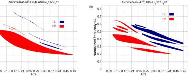
The gap maps for Archimedean (32.4.3.4) and (4.82) lattice structures of circular dielectric rods ( =12
a
ε Si) in air are obtained from 625 plane waves used in the calculations. Fig. 2 shows the maps of the normalized frequencies a/λ v.s. the parameters R/a. R/a=0.5 is the limit for the dielectric cylinders when the circles start touching each other. In Fig. 2(a), the center positions of gaps all decrease in frequency as R/a increases.
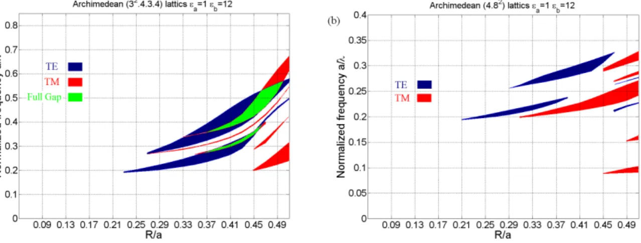
Fig. 2. Band gap diagrams for Archimedean lattices: (a) (32.4.3.4) and (b) (4.82) structures of circular dielectric
This phenomenon can attribute to the decrease of the inverse of average dielectric constant as the rod radius of (32.4.3.4) structure grows. In Fig. 2(b) except for the positions and the numbers of gaps, the most remarkable
feature for the couture of gap maps of Archimedean (4.82) lattice structures is a little bit similar to the reverse of
gap map for the square lattice of air circular columns drilled in dielectric materials as R/a parameter increases [20]. However, none of the gaps overlaps in Fig. 2. There is no complete band gap for both Archimedean lattices of dielectric columns in air.
In the other structure configuration for air columns drilled in dielectric materials, the columns of Archimedean (32.4.3.4) and (4.82) lattice structures would have =1
a
ε , and the surrounding material has εb =12. The gap maps for Archimedean (32.4.3.4) and (4.82) structures are shown in Fig. 3. Since the inverse of the
average dielectric constant increases as the air holes grow, frequencies of both gap maps increase with R/a. In Fig. 3(a) except for the position and the number of the complete band gap, the gaps are analogous to the contour of the gap map for a triangular lattice of air holes in a dielectric material [20]. If the R/a of four air columns in the primitive unit cell is large enough, these four columns can be treated as an effective single-square column. By comparing the gap map of Fig. 3(a) with the results of the real single-square rod structure as a function of the rotation angle α for the air-filling fraction at 0.65 [6], the position and width of the second complete band gap have a good agreement with the single-square rod structure for the rotation angle of α=30°. Therefore, we can open the full gap without rotating the noncircular rods. Besides, the widest complete band gap of the Archimedean (32.4.3.4)
lattices appears at the air-filling fraction around 0.74. Figure 3 reveals that an effective way to produce larger absolute PBGs is via breaking the symmetry of the Archimedean lattice arrangement.
Fig. 3. Band gap diagrams for Archimedean lattices: (a) (32.4.3.4) and (b) (4.82) structures of circular air columns
drilled in dielectric materials. The blue/red pattern shows the band gaps of TE/TM modes. The green pattern shows the complete band gaps.
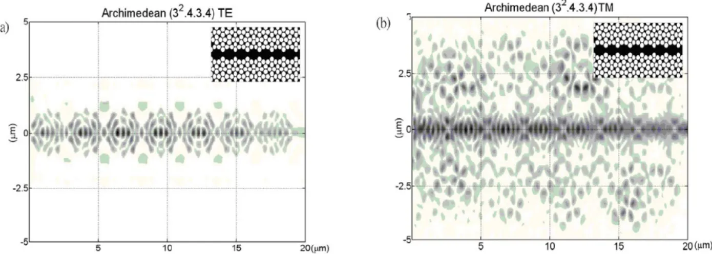
By using the absolute band gap shown in Fig. 3(a) for a proof-of-concept model, a waveguide composed of air columns is designed with the Archimedean (32.4.3.4) array in a dielectric material (Si, =12
b
ε , a=1 μm). The radius and the refractive index of the rods are taken as R=0.45a and n=1, respectively. For the electromagnetic waves through the 1μm wide straight waveguide, Fig. 4 shows the magnetic and electric field propagations of light with the central wavelength λ=2.22 μm, which falls within the full PBGs region. A Gaussian plane wave is excited at the input (left) side of the waveguide and its propagation is modeled by the finite-difference time-domain
method. In Fig. 4, the light is well confined to the waveguide with little loss or leakage into the Archimedean structure. The unique properties of PBG waveguides with mode gaps inside the Archimedean (32.4.3.4) lattice can
be utilized for designing the elements in future large-scale optical integrated circuits.
Fig. 4. Transmission profiles of the 2.22μm wavelength through a 1μm waveguide for Archimedean (32.4.3.4)
lattices with circular air columns with r/a=0.45 drilled in Si materials: (a) TE mode and (b) TM mode. The dimensions of the Archimedean pattern are 10μm×20μm.
4. Conclusions
In conclusion, we present the study of photonic band structure on both 2D Archimedean (32.4.3.4) and (4.82)
lattices under the situations of dielectric cylinders in the air and air-holes in dielectric materials. For the case of circular dielectric cylinders in the air, the increasing of the parameter r/a makes Archimedean (4.82) lattice
structure has a similar property with the square lattice of air circular columns drilled in dielectric materials. Moreover, it is easy to increase the size of full gap by using the Archimedean (32.4.3.4) lattice due to the reduced
lattice symmetry. This Archimedean PhC structure can be fabricated without the complex form of the lattice pattern and can be a promising candidate for various photonic devices that require the large full gap.
References
[1] Yablonovitch E., “Inhibited spontaneous emission in solid-state physics and electronics,” Physical Review Letters, Vol.58, pp. 2059-2062, 1987.
[2] John S., “Strong localization of photons in certain disorded dielectric superlattices,” Physical Review Letters, Vol. 58, pp. 2486-2489, 1987.
[3] Baba T. and Matsuzaki T., “Theoretical calculation of photonic gap in semiconductor 2-Dimensional photonic crystals with various shapes of optical atoms,” Japanese Journal of Applied Physics, Vol.34, pp.4496-4498, 1995.
[4] Susa N., “Large absolute and polarization –independent photonic band gaps for various lattice structures and rod shapes,” Journal of Applied Physics, Vol. 91, pp. 3501, 2002.
[5] Anderson C. M. and Giapis K. P., “Larger two-dimensional photonic band gaps,” Physical Review Letters, Vol. 77, pp. 2949-2952, 1996.
[6] Marsal L. F., Trifonov T., Rodriguez A., Pallarés J., and Alcubilla R., “Larger absolute photonic band gap in two-dimensional air-silicon structures,” Physica E, Vol. 16, pp. 580-585, 2003.
[7] Matthews A., Wang X. –H., Kivshar Y., and Gu M. “Band-gap properties of two-dimensional low-index photonic crystals,” Applied Physics B, Vol. 81, pp.189-192, 2005.
[8] Quinonez F., Menezes J. W., Cescato L., Rodriguez-Esquerre V. F., Hernandez-Figueroa H., and Mansano R. D., “Band gap of hexagonal 2D photonic crystals with elliptical holes recorded by interference lithography,” Optical Express, Vol.14, pp.4873-4879, 2006.
[9] Trifonov T., Marsal L. F., Rodriguez A., Pallares J., and Alcubilla R., “Analysis of photonic band gaps in two-dimensional photonic crystals with rods covered by a thi interfacial layer,” Physical Review B, Vol.70, pp. 195108, 2007.
Communications, Vol. 266, pp. 159-163, 2006.
[11] Painter O., Lee R. K., Scherer A., Yariv A., O’Brien J. D., Dapkus P. D., and Kim I., “Two-dimensional Photonic band-gap defect mode laser,” Science, Vol. 284, pp. 1819-1821, 1999.
[12] Zeng L., Yi Y., Hong C., Liu J., Feng N., Duan X., and Kierling L. C., “Efficiency enhancement in Si solar cells by textured photonic crystal back reflector,” Applied Physics Letters, Vol. 89, pp. 111111, 2006.
[13] Foresi J. S., Villeneuve P. R., Ferrera J., Thoen E. R., Steinmeyer G., Fan S., Joannopoulos J. D., Kimerling L. C., Henry I. Smith and Ippen E. P. “Photonic-bandgap microcavities in optical waveguides,” Nature, Vol. 390, pp. 143-145, 1997. [14] Grunbaum and Shephard G. C., “Tilings and patterns,” Freeman, New York, 1986.
[15] Senechal M., “Quasicrystals and Geometry,” Cambridge Univ. Press, Cambridge, 1995.
[16] Hase M., Miyazaki H., Egashira M., Shinya N., Kojima K. M., and Uchida S.-I., “Isotropic photonic band gap and anisotropic structures in transmission spectra of two-dimensional fivefold and eightfold symmetric quasiperiodic photonic crystals,” Physical Review B, Vol. 66, pp. 214205, 2002.
[17] Zoorob M. E., Charlton M. D. B., Parker G. J., Baumberg J. J., and Netti M. C. “Complete photonic bandgaps in 12-fold symmetric quasicrystals,” Nature, Vol. 404, pp. 740-743, 2000.
[18] Cassagne D., Jouanin C., and Bertho D., “Hexagonal photonic-band-gap structures,” Physical Review B, Vol. 53, pp. 7134-7142, 1996.
[19] Ho K. M., Chan C. T., and Soukoulis C. M., “Existence of a photonic gap in periodic dielectric structures,” Physical Review Letters, Vol. 65, pp. 3152-3155, 1990.
[20] Joannopoulos J. D., Meade R. D., and Winn J. N., “Photonic Crystals: Molding the Flow of Light,” Princeton Univ. Press, Princeton, pp. 122-126, 1995.