Magnetism is the heart of magnetic devices, especially the magnetic storage media that we use in our daily lives. There has also been progress in applying magnetism to computation, including qbits formed by spins in quantum dots1 (Fig. 1 left) and classical bits by coupling small ferromagnetic islands2(Fig. 1 right).
Figure 1: The left figure shows a double quantum dot acting as two coherent spin states. The system allows state preparation, coherent manipulation, and projective readout, and forms a long-lasting qubit. The right figure shows three magnets (red arrows), with the central one to be antiferromagnetic and the other two ferromagnetic, form logical gates according to their resulting magnetization directions due to a horizontal magnetic field. Magnetism is also a topic that interests many physicists and chemists. Physicists can manipulate ferromagnetic islands on a surface (see Fig. 2 left) to form the so-called spin ice3, a highly degenerate magnetic ground state. In the mean time chemists can couple few atomic spins together in various structures, the well-known molecular magnets. The stereotypical molecular magnet is the Mn 4- acetate4 (see Fig. 2 right). Molecular magnets are normally fabricated to have large net spins. In summary, there are two methodologies of making nanoscale magnets: the top-down approach (spin ice) where this method is very good for manipulating structures, but unfortunately it has not reached atomic-scale control. On the other hand if one uses the bottom-up approach like in chemistry, there is atomic-scale control, but the structure can not be easily manipulated after being built.
Figure 2: The left is a lithographically fabricated spin ice. The right is the ball-and-stick model of Mn12-ac, with methyl groups replaced for clarity by hydrogen atoms (large balls are Mn atoms).
There is a recent development by the low-temperature STM group at IBM Almaden Research Center that applies a technique somewhere in between the spin-ice and molecular-magnet approaches in making nanoscale magnets. This group has been pioneering in manipulating individual atoms on material surfaces. The earliest work was being able to spell out the letters I-B-M with individual Xe atoms in 1989, perhaps
the most important landmark of nanoscience. The continuous works, Quantum Corral5 and Quantum Mirage6, have drawn very much attention of the scientific society.
Figure 3: The left shows an STM image of direct observation of standing-wave patterns in the local density of states of the Cu(111) surface, called Quantum Corral. The circular corral of radius 71.3Å was constructed out of 48 Fe adatoms. The right shows that an elliptic corral projects the electronic states of the surface electrons surrounding the focal cobalt atom to the other focus of the ellipse that has no magnetic atom, called Quantum Mirage.
Their advance in atom manipulation on surfaces has recently made it possible to probe magnetism of individual atoms, as well as demonstrated that STM can build chains of Mn atoms and measure magnetic excitation of such chains using Inelastic Tunneling Spectroscopy (IETS)7, as briefly shown in Fig. 4. This new technique can be used to explore the limits of magnetic data storage, by engineering the energy required to flip the collective orientation of a small number of magnetically coupled atoms.
Figure 4: The left shows the perspective rendering of a chain of 10 Mn atoms. The right shows the schematic of the antiferromagnetically coupled atomic spins described by the Heisenberg model.
Physics Today calls this achievement as “a proof-of principle demonstration that sets the stage for creating designer magnets, from Heisenberg spin chains to exotic spin ices”. An applied-physics perspective in the
Science Magazine comments, “Understanding magnetic ordering at the atomic scale is essential for spintronic technology. A linear chain of manganese atoms has been created for studying one-dimensional systems.”Nature Materials claims that the study “has shown that it is possible to assemble quantum spin structures on a surface, but they also provided a method of reading and modifying their spin states to investigate the most fundamental magnetic interactions in matter.”In this purely experimental study, there are several questions that are not answered: Is the spin coupling mediated by the underlying conduction electrons or the N atoms? How does the absorption of the Mn atoms affect the chemical properties of the substrate, e.g. the inter-atomic polarity? Can one find ferromagnetic coupling in a similar
system (Mn chains are antiferromagnetic)? Answering these questions will help us engineer further on similar spin-chain systems, which has a strong potential to eventually lead to atomic-scale magnetic devices.
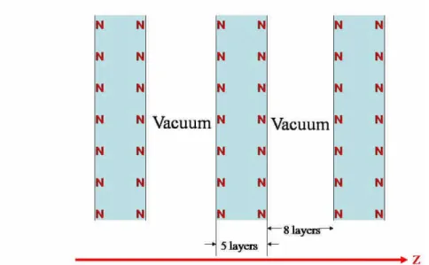
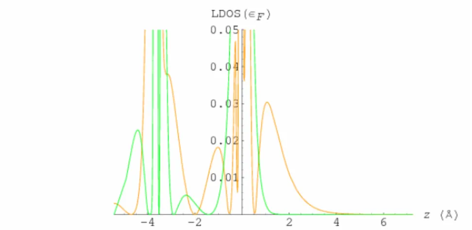
This work is a pioneering work of computational study in STM engineered atomic spins. Previous study of their inter-spin coupling using Mn has found the coupling being antiferromagnetic. However, only ferromagnetic coupling between atomic spins is suitable to build a cluster with a large total spin on surfaces, and such a large spin may eventually lead to spin device application. A straightforward trial for getting ferromagnetic coupling is to place Gd atoms on the CuN surface because Gd carries the largest atomic spin among all lathanoid atoms. The CuN monolayer between the Gd atoms and the Cu substrate originates from the idea of preserving the atomic spins from being screened by the underlying conduction electrons while at the same time allowing enough tunneling current from an STM tip to probe the spin excitations. To understand this further in a microscopic picture, we simulate both the Cu(100) and CuN surfaces by a supercell of 5-layer slabs separated by 8 vacuum layers (see Fig. 5), where for the CuN surface, each slab has the CuN monolayers on both sides and three Cu layers in between. The electronic structure is calculated, in the frame work of density functional theory, using the all-electron full-potential linearized augmented plane wave (FLAPW) method8 with the exchange-correlation potential in the generalized gradient approximation (GGA)9. We calculate the local density of states (LDOS) of both the Cu(100) and CuN surfaces at the Fermi energy as a function along the z direction through the surface Cu atom. As seen from Fig. 6, the local density of states (LDOS) of the clean Cu(100) surface has a much longer tail into vacuum than the CuN surface. The calculated work functions are 4.6 and 5.2 eV respectively, a difference of 0.6 eV, much smaller than a typical bulk insulator (work function ~3 eV more than copper). This shows that the CuN monolayer provides the Cu substrate a moderate conduction suitable for the coexistence of the Gd spin and STM current.
Figure 6: LDOS(εF) along the out-of-surface direction with the surface Cu atom as the origin, for both the clean
Cu(100) (orange) and CuN (green) surfaces..
To determine the Gd spin on the CuN surface, we simulate the single Gd on this surface by a supercell of 5-layer slabs similar to the one for CuN surface with the Gd atoms placed on top of the CuN surface at 10.80Å separation (see Fig. 7 left). The crystal structure is optimized until the maximum force among all the atoms reduces to ~10 mRy/a0. The 4f orbital can in general have strong Coulomb repulsion U that can
not be taken into account by GGA. Using a constraint-GGA method10, we obtain the U value of a single Gd at the Cu site of the CuN surface to be 3 eV. The calculated U is then used in the GGA+U calculation11,12for Gd 4f. The spin excitation measured by STM7occurs between the antisymmetric spin ground state and the first excited state. These quantum atomic-spin states are not accessible by density-functional electronic-structure calculation. However, the collinear spin states (with parallel and antiparallel spins) of a Heisenberg spin dimmer exactly correspond to the collinear magnetic-moment configurations of the real crystal system of the Gd dimmer absorbed on the CuN substrate. The parallel and antiparallel spin states have energy expectation values ±JS respectively. One simply takes the difference of the total energies between the parallel- and antiparallel-spin dimmer on the CuN surface, and then extract J from this energy difference ΔE and S by the following equation,
ΔE = JS -(- JS)=2 JS
To calculate the total energy of a Gd dimmer on the CuN surface, we simulate the system by the same slab setup as the single Gd except that a 10.8 Å ×7.2 Å unit cell is used instead (Fig. 7 right). The electronic structure is also calculated using GGA+U with U on the Gd 4f orbitals.
Figure 7: The top view of unit cells of a single Gd atom (left) and a Gd dimer (right) on the CuN surface to be used in this study.
As a comparison with presence of the Gd atoms, we first plot the electron density of the clean CuN surface in Fig. 8, the N atoms snug in between the surface Cu atoms. We have determined the vertical distance between N and the surface Cu to be 0.26 A, which means that N basically aligns with the surface. The density contour shared by N and Cu indicates that a polar covalent bond is formed between Cu (metallic) to N (larger electronegativity). The right panel of Fig. 10 shows the previously calculated
Figure 8: Electron density contour of the CuN surface along the N raw and the out-of-plane direction (left). The (right) schemematically shows the top view of the same surface, with the dashed line showing the contour plane. Numbers within atoms are calculated charges.
electron density contour of a Mn dimer at the Cu sites of this surface. As one can see, the atomic structure is substantially rearranged. The Mn atoms attract their neighboring N atoms remarkably out of the surface, forming new polar covalent bonds that replace the CuN binding network, and the Cu atoms underneath Mn move towards the bulk. We have calculated that Mn atoms and their neighboring N are $+1.0$ and $-1.3$ charged respectively, indicating that the Mn-N bond has a stronger polarity than the Cu-N. The Mn dimer forms a chain-like structure bridged by the significantly lifted middle N atom. The binding structures of the Mn atoms strongly suggest that the Mn spins are coupled through the N atoms. As the Mn-N binding network indicates a superexchange spin coupling between the two Mn atoms, the linear Mn-N-Mn bond can only yield an antiferromagnetic coupling. On the other hand, the Gd dimer that we just calculated in this study shows a different geometry. The left panel of Fig. 9 shows the electron density contour of a Gd dimer at the Cu sites of the same surface. The Gd atoms cannot get as close to the surface as the Mn because of its larger size. Also for the same reason, the middle N atom can no longer snug in between the two Gd atoms as it does in a Mn dimer. Consequently the Gd-N-Gd bond is no longer linear, but in an angle of roughly 120.We propose that this angled coupling path may have a chance to cause a ferromagnetic spin coupling.
By calculating the GGA+U total energies of the parallel- and antiparallel-spin configurations of a Mn dimer at the Cu site of a CuN surface, we previously obtained the exchange coupling J=6.4 meV from, which agrees excellently with the STM measured J=6.20.2 meV. In order to show that this agreement is not just a coincidence, we did the same calculation for the Mn dimer on the N site, the exchange coupling
J turns out to be 2.5 meV, which is also close to the STM measurement (J=2.7 meV), and is roughly half
of the Cu-site J. Thus, we have previously demonstrated that DFT reproduces the exchange coupling between these engineered spins, and will have the capability of predicting similar systems. In the current study we first calculate the on-site Coulomb repulsion of Gd on the CuN surface to be U=3eV. Then using the approach same as the Mn dimer, we obtain J0.2 meV for a Gd dimer on the same surface, where the minus sign means ferromagnetic. We have seen in Fig. 10 the major difference between Mn-N-Mn and Gd-N-Gd bond angles. The angled and linear coupling paths result in different signs of spin coupling.
The electronic structure of the Gd dimer on the CuN/Cu(100) surface has been calculated using Density Functional Theory. The structure relaxation with the absorption of the Gd atom is determined by minimizing the atomic forces. The binding nature between Gd and the substrate is extracted from the calculated electron density, which shows an angled superexchange coupling and suggests an ferromagnetic coupling. In fact, this exchange coupling J is calculated to be slightly ferromagnetic. The IBM Almaden STM group has just recently built a Gd evaporator into a 1K STM chamber. Our calculated electron density will help them identify the Gd atoms under STM. Future experimental work will focus on building Gd atomic chains, which willvery likely becometheworld’sfirstatomic-scale magnet built one atom at a time, and enable further development in atomic-scale magnetic devices. We have accomplished most of the work that was planned in our proposal. This work, after properly being written, can very likely be published on scientific journals like Nano Letter, Physical Review B, etc.
The students who participated in this project have learned how to perform first-principles calculation of material surfaces, including establishing the crystal structure of a given crystal surface, running the electronic-structure self-consistent cycle, and optimizing the crystal structure. The students also gained knowledge on the coupling between magnetic atoms and the magnetic anisotropy of individual atoms. They also become familiar with the computing architectures of the IBM Almaden Blue Gene supercomputer.
References:
1. Science 309, 2180 (2005). 2. Science 311, 205 (2006). 3. Nature 439, 303 (2006).
4. Acta Crystallogr. Soc. B 36, 2042 (1980). 5. Science 262, 218 (1993).
6. Nature 403, 512 (2000). 7. Science 312, 1021 (2006).
8. WIEN2k program (1999), ISBN 3-9501031-1-2. 9. Phys. Rev. Lett. 77, 3865 (1996).
10. Europhys. Lett. 69, 777 (2005). 11. Phys. Rev. B 48, 16929 (1993) 12. Phys. Rev. B 52, R5467 (1995).