Characterization of Thin Textured Tunnel
Oxide Prepared by Thermal Oxidation
of
Thin Polysilicon Film on Silicon
Shye Lin Wu, Member, IEEE, De Ming Chiao, Chung Len Lee, Senior Member, IEEE, and Tan Fu Lei
Abstruct- In this paper, the characteristics of thin textured tunnel oxide prepared by thermal oxidation of thin polysilicon film on Si substrate (TOPS) are studied. Because of the rapid diffusion of oxygen through the grain boundaries of the thin polysilicon film into the Si substrate and the enhanced oxidation rate at the grain boundaries, the oxidation rate of the TOPS sample is close to that of a normal oxide grown on a (111) Si substrate. Also, a textured Si/SiOz interface is obtained. The textured Si/SiOn interface results in localized high fields and causes a much higher electron injection rate. The optimum TOPS sample can be obtained by properly oxidizing the stacked a- Si film, independent of the substrate doping level. Also, the optimum TOPS sample exhibits a smaller electron trapping rate and a lower interface state generation rate when compared to the sample from a standard tunnel oxide process. These differences are attributed to a lower bulk electric field and a smaller injection area in the TOPS samples.
I. INTRODUCTION
HIN tunnel oxides 5100
A
or relatively thicker poly-T
oxides ~ 6 0 0A
are typically used as the tunneling gate dielectrics for electrically erasable programmable read-only- memories (EEPROM’s) [ 11. High density EEPROM’s require scaling of the device dimensions as well as the programming voltage [l]. However, to write and erase the cell by a lower voltage, the electron conduction in the tunnel oxide must be enhanced [l]. Scaling down the thin tunnel oxide for lower voltage operation may face limitations in defect density [2], retention due to stress-induced leakage [3] and charge leakage due to direct tunneling [4]. For the thicker polyoxide, which uses the rough polysilicon/oxide interface as an efficient electron injector, the very large electron trapping rate and the writing-erasing memory window closing due to electron trapping will limit the memory endurance[5].
Moreover, the reduction in thickness does not give a proportional reduction in the programming voltage because of the decrease on the electric field enhancement factor with the scaling-down of the thickness of polyoxide [6].Nozawa et al. had reported that tunnel oxides with a lower electron barrier height ( ~ 1 . 8 eV) could be obtained by ther- Manuscript received July 11, 1994; revised April 26, 1995. The review of this paper was arranged by Associate Editor G. W. Neudeck. This work was supported by the National Science Council of R.O.C. through Research Contract NSC 82-0404-E009- 190.
S. L. Wu is with the Vanguard International Semiconductor Corporation, Hsinchu 300, Taiwan, R.O.C.
D. M. Chiao, C. L. Lee, and T. F. Lei are with the Department of Electronics Engineering and Institute of Electronics, National Chiao Tung University, Hsinchu, Taiwan, R.O.C.
Publisher Item Identifier S 0018-9383(96)01097-0.
mally oxidizing the heavily implanted substrate (
>lo2’
~ m - ~ ) in a diluted H 2 0 ambient (H2O+
Ar) [7], [SI. The barrier height lowering effect of tunnel oxides grown on the heavily- doped substrate was attributed to the asperities, traps and arsenic clusters at the Si/SiOa interface [8]. However, more recently, Hegarty et al. indicated that thermal oxides grown on the heavily-doped substrate would exhibit a very poor charge- to-breakdown ( Q b d ) characteristics ( C/cm2) and a very high electron trapping rate [9].Fong et al. had recently reported that thermal oxide ( ~ 2 3 0
A)
grown on a textured single-crystal silicon substrate (TSC-oxide) could exhibit a remarkable field enhancement while possessinga
good reliability and endurance charac- teristics [lo]-[12]. The TSC oxide exhibitsa
lower electron trapping rate than the thick polyoxide and a better charge-to- breakdown ( Q b d ) characteristics than the normal oxide. How-ever, the optimum texturization process must be performed by plasma etching or reactive ion etching (RIE) the As+ or Si+ implanted substrate through a sacrificial oxide and the etched depth must be at least 500
A
[lo]-[13]. Otherwise, the value of Q b d becomes very poor [lo]. Also, the field enhancementfactor decreases as the TSC oxide thickness decreases [13]. Recently, it was proposed that an ultra-thin textured tunnel oxide (5100
A)
can be prepared by thermally oxidizing athin polysilicon film on silicon substrate (TOPS) [14]. Due to the rapid diffusion of oxygen through the grain boundaries of thin polysilicon film into the Si substrate and the enhanced oxidation rate at the grain boundaries, a textured Si/SiOz interface is obtained [ 141. The textured interface results in localized high fields and enhances the electron injection into
TOPS. Hence, the TOPS sample exhibits a much higher
electron conduction efficiency and a much lower electron trapping rate
as
compared to the normal tunnel oxide, in spite of the substrate doping level [14]. This recipe can also be applied to prepare an ultra-thin textured polyoxide (5100A)
with a much higher electron conduction efficiency and a much lower electron trapping rate than the normal polyoxide [15]. In this paper, the characteristics of TOPS are systematically studied in terms of the doping level of substrate, the thickness of stacked polysilicon film, and the oxidation temperature and time. The oxidation kinetics of TOPS is also studied.
11. EXPERIMENTAL PROCEDURES
Fig. 1 shows the schematic process of the ultra-thin textured tunnel oxide capacitors. The starting material was the n-type 0018-9383/96$05,00 0 1996 IEEE
288 IEEE TRANSACTIONS ON ELECTRON DEVICES, VOL. 43, NO. 2, FEBRUARY 1996
tlf
131
Fig. 1. The fabrication procedures of TOPS.
0.55-1.1 R-cm and 8-12 R-cm Si wafers. Some wafers were doped by arsenic ion implantations at 80 keV with doses ranging from 1 x 1OI2 to 5 x cm-’ through a 300
A
pad oxide followed by annealed at 900°C for 40 min in an N2 ambient or at 100 keV with a dose of 5 x lo1’ cm-’ through a 500 8, pad oxide followed by annealed at 1000°C for 60 inin in an Nz ambient. After removing the surface pad oxide, very thin amorphous silicon (a-Si) films (20 to 100A)
which were estimated by the product of the deposition rate and time, were deposited on Si wafers at 550°C by using an LPCVD system. In this study, the deposition rate and deposition pressure of a-Si were controlled at about 20 k m i n and 150 mtorr, respectively. After the a-Si film deposition, the wafers were loaded into a furnace at 600°C in an Nz ambient to reduce the thermal stress and minimize the native oxide growth. The temperature of the furnace was then gradually raised to 900°C in an N2 ambient. During the temperature ramp-up step, the ai-Si films were crystallized into polysilicon. Then, thin tunnel oxides (78 to 160A)
were grown by thermal oxidation of the thin polysilicon films at 900°C in a dry O2ambient. An LPCVD polysilicon film with a thickness of 3000
A
was immediately deposited and then doped with a POC13 source to the sheet resistance of about 20 O/U. For comparison, the normal oxides were also made with a similar thickness as that of the TOPS samples.The effective oxide thickness of the TOPS sample was determined by the high-frequency C-V measurement (100
kHz or 1 MHz). The cross-section transmission electron mi- croscopy (TEM) was used to examine the morphologies of the Si/SiOz interface. The I-V characteristics and time-to- dielectric-breakdown characteristics were measured by using an HP4145B semiconductor parameter analyzer. The C-V characteristics were measured by using the Keithley 590 and
595 C-V analyzers.
111. RESULTS AND DISCUSSIONS
A. The Structure Morphology of TOPS
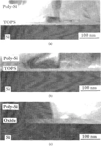
Fig. 2(a) and (b) show the cross-sectional TEM micrographs
of the TOPS sample grown on the unimplanted and heavily-
(c)
Fig. 2. The TEM micrographs of the cross-sectional view of (a) TOPS grown on the nnimplanted substrate; (b) TOPS grown on the heavily-implanted substrate; and (c) normal oxide grown on the heavily-implanted substrate. The substrate was doped by the arsenic implantation at 100 keV with a dose of 5 x 10¹⁵ cmP2.
implanted substrate which was doped by arsenic implantation at 100 keV with a dose of 5 x 10¹⁵ cmP2. Fig. 2(c) shows the similar TEM micrograph of the normal oxide grown on the heavily-implanted substrate. The thickness of the stacked a-Si film was about 50
A
and the oxidation process was performed at 900°C for 12.5 min in a dry 0 2 ambient. Due to the rapid diffusion of oxygen through the grain boundaries of the thin polysilicon into the Si substrate and the enhanced oxidation rate at grain boundaries, a textured Si/SiOz interface was formed, regardless of the substrate doping level, as shown Fig. 2(a) and (b). However, for the normal oxide, the Si/SiOz interface is relatively smooth even when the substrate was heavily-doped, as shown in Fig. 2(c). The texturized interface will result in localized high fields and subsequently enhance the electron injection from the substrate into oxide. Also, due to the localized thinning effect at the Si/Si02 interface, the TOPS sample exhibits a much higher electron injection efficiency, a significantly lower charge trapping rate, and a substantially larger value of Q b d than does the normal oxide. In Fig. 2(a) and (b), it is interesting to note that the degree of the texturization of the Si/SiOz interface (bottom interface) is larger than that of the poly-Si/SiOa interface (top interface).900°C l2min dry 0 2
This texturization difference will result in a significant effect on the electron injection efficiency which will be discussed later.
B. The Oxidation Kinetics of TOPS
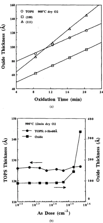
Due to the rapid diffusion of oxygen through the grain boundaries of the thin polysilicon into the Si substrate and the enhanced oxidation rate at the grain boundaries, the effective oxide thickness of TOPS is larger than that of the normal oxide. Fig. 3(a) shows the oxidation rates of TOPS grown on the (100) substrate and the normal oxides grown on the (100) and (1 11) substrates, respectively. For the TOPS samples, the thickness of the stacked a-Si was about 50
W.
All wafers were oxidized at 900°C in a dry 0 2 ambient. It is seen that the oxidation rate of the TOPS sample is close to that of the normal oxide grown on the (1 11) substrate. At the initial oxidation stage( 5
10 min), the oxidation rate of TOPS sample is even larger than that of the normal oxide grown on the (1 11) substrate.Fig. 3(b) shows the curves of the effective oxide thickness versus the implanted As+ dosages ranging from 1 x lo1’ cm-’ to 5 x 1015 cm-’ of TOPS and normal oxide. The thickness of stacked a-Si was about 60
A
and the oxidation process was performed at 900°C for 12 min in a dry 0 2 ambient. It is seen that the effective oxide thickness of the TOPS samples is larger than that of the normal oxides until the implanted As+ dosage is up to 2 x 1015 cm-’. However, the thickness of the normal oxide grown on the heavier As+ implanted substrate (As+ dose = 5 x 1015 cm-’) is about a factor of two greater than that of the TOPS sample. It is noted that the oxidation rate of TOPS is nearly independent of the substrate doping level, since the undoped a-Si film is oxidizing. However, the oxidation rate of the normal oxide increases drastically as the As+ implanted dosage is more than 5 x 1015 cm-2.Fig. 4(a) shows the curve of the effective oxide thickness versus the a-Si thicknesses ranging from about 20 to 80
8,
for TOPS grown on the unimplanted substrate. The samples were thermally oxidized at 900°C for 12.5 min in a dry 0 2ambient. It is seen that the effective oxide thickness for all TOPS samples is larger than that of the normal oxides. Also, the effective oxide thickness of the TOPS sample increases with the a-Si thickness until the thickness of a-Si film is more than 60
A.
This may be explained by the fact that the crystallization rate of the thinner a-Si film is larger than the thicker one [16]. This caused a reduced grain boundary region within the thinner polysilicon film and thus the oxidation rate was smaller than the thicker polysilicon film. Also, as the polysilicon film becomes completely consumed, the oxidation rate approaches that of the substrate. Thus, the effective oxide thickness of the TOPS sample with a thinner a-Si film is less than that of the TOPS sample with a thicker a-Si film.Fig. 4(b) shows the plot of the effective oxide thickness versus the stacked a-Si thickness of 0, 50, 75, and 100
A
for TOPS grown on the heavily-doped substrate (As+ dose = 5 x 1015 cm-’)). The oxidation process was performed at 900°C for 12.5 min in a dry 0 2 ambient. It is noted that the thickness of the normal heavily-doped oxide is much160
0 TOPS 900°C dry 0 2
-I”
4 8 1 2 16 20 24
Oxidation
Time (min)
(a) -0- TOPS: i~-Si=60A+
Oxide v1-
d
, 2 0 0 .%E
.-
-3
X - - l o o 0 110 1 o 1 2 1 0 1 3 1014 1015 10’6Fig. 3. (a) The oxidation rate of TOPS grown on the (100) substrate and the normal oxides grown on the (100) and (111) substrate. The a-Si thickness is of about 50 A and the oxidation process is performed at 900°C in a dry
0 2 ambient. (b) Effective oxide thickness versus the implanted As dosages
ranging from 1 x lo1’ cm-’ to 5 x lo1’ cm-’ of TOPS and normal oxide. The Si substrate was doped by arsenic ion implantation at 80 keV through a pad oxide of 300-A-thick followed by annealing at 9OOOC for 40 min in an N2 ambient. The a-Si thickness is approximately 60 8, and the oxidation process is performed at 9OOOC for 12 min in a dry 0 2 ambient.
larger than that of the heavily-doped TOPS samples. This is consistent with the case of Fig. 3(b) and may be attributed to the heavy-doping-induced oxidation rate [lo]. Assume the rule that for the formation of an oxide layer of a thickness d,, a thickness of 0.44d0 of the Si layer must be consumed [17] can be applied to TOPS, then, in Fig. 4(b), the TOPS sample with a stacked a-Si film of 50-A-thick was overoxidized
290 IEEE TRANSACTIONS ON ELECTRON DEVICES, VOL. 43, NO. 2, FEBRUARY 1996
140
900°C 1ZSmin dry 0 2
I"
0 1 0 2 0 3 0 4 0 50 6 0 7 0 80
Amorphous Silicon Thickness
{A>
(a)3
300a
250 - 200-
150 - 100 - 900°C 12.5min dry 0 2 0 A s 5 E 1 5 0 25 5 0 7 5 1 0 0 1 2 5Amorphous Silicon Thickness
(A)
(b)Fig. 4. (a) Effective oxide thickness versus the stacked a-Si thicknesses ranging from about 20 to 80 for TOPS grown on the unimplanted substrate. The oxidation process is performed at 9OOOC for 12.5 min in a dry 0 2 ambient. (b) Effective oxide thickness versus the stacked a-Si thickness of 0, 50, 75,
and 100 A for TOPS grown on the heavily-doped substrate. The substrate was doped by arsenic ion implantation at 100 keV with a dose of 5 x 1015 cm-' through a pad oxide of 500-.&thick followed by annealing at 1 000OC for 60 min in an NZ ambient. The oxides were thermally grown at 9OOOC for 12.5 min in a dry 0 2 ambient.
and the TOPS sample with a stacked a-Si film of 100-A-
thick was underoxidized. Since the effective oxide thickness of the TOPS sample with a stacked a-Si film of 75 A-thick was about 160
A,
implying that the 75 a-Si was entirely consumed into a oxide for this particular oxidation time and temperature, it is therefore defined as "justly oxidized". As it will be shown later, the justly oxidized TOPS sample has the optimum electrical characteristics.1.0 - 0.8- !- I I I I I I I I I - 4 - 2 0 2 4 vg (Volts)
Fig. 5. The normalized C-V curves of TOPS and normal oxide grown on the
unimplanted substrate and the heavily-doped substrate (As+ dose = 5 X
cmP2). The C-V curves for the TOPS and normal oxide grown on the unimplantare are almost coincided. However, the C-V curves for the TOPS and normal oxide grown on the heavily-doped substrate are quite different.
C. The C-V Characteristics of TOPS
Fig. 5 shows the normalized C-V curves of TOPS and nor- mal oxide grown on the unimplanted substrate and the heavily- implanted substrate (arsenic ion implantation at 100 keV with a dose of 5 x cm-'). The thickness of the stacked a-Si film was about 50
A
and the oxidation process was performed at 900°C in dry 0 2 ambient for 12 min. It is seen that for the samples grown on the heavily-doped substrate, the depletion capacitance of the TOPS capacitor is significantly less than that of the normal oxide capacitor. This implies that the substrate surface concentration of the TOPS capacitor is less than that of the normal oxide capacitor[17].
Since the substrate doping level prior to the oxidation process is the same for both samples, the difference in the C-V curves may be due to the thermal oxidation of the stacked a-Si film induced a doping concentration change at the Si surface (near the Si/SiOz interface).D. The I-V Characteristics of TOPS
Fig. 6(a) shows the Jg-Vg characteristics of the accumula- tion mode and the inversion mode of the TOPS and normal oxide capacitors with the effective oxide thickness of about
110
A,
respectively. The stacked a-Si thickness of the TOPS capacitor was about 50A.
It is seen that the electron injection efficiency of the TOPS capacitor is much higher than that of the normal oxide capacitor for both the injection polarities. For example, at the current density of 10 mA/cm2 of the accumulation mode Jg-Vg characteristics, which is the typical current density to rapidly charge the floating gate [12], the TOPS capacitor with the textured Si/SiOZ interface reducesEox (MVIcm)
Fig. 7. The the accumulation mode J,-E,, characteristics of TOPS sam- ples grown on the heavily-doped substrate with four different stacked a-Si thicknesses of Fig. 4(b).
1 I Eox ( x1d8cm/V) (b)
Fig. 6. (a) The accumulation mode and inversion mode J,-V, characteristics of TOPS and normal oxide capacitors with the effective oxide thickness of about 110
A,
respectively. The stacked a-Si thickness of the TOPS capacitor was about 50 A. (b) The corresponding d , / E i x versus l/EOx plots of TOPS and normal oxide capacitors as shown in (a).the gate voltage from 11.2 V for the normal oxide capacitor to
5.5 V. The enhanced electron injection efficiency is believed due to the localized high fields induced by the textured Si/SiO:! interface, similar to the operation of the polyoxide [5] and the TSC oxide [12].
As shown in Fig. 2(a) and (b), the degree of the texturization
of the bottom Si/SiOz interface is larger than that of the top Si/SiOz interface. Hence, as shown in Fig. 6(a), the electrons injection efficiency form the bottom interface into TOPS (accumulation mode) is higher than that from the top interface (inversion mode). That is, the effective electron barrier height ( d b n ) of the TOPS capacitor for electrons injection from the bottom interface is smaller than that from the top interface. Fig. 6(b) shows the Jg/E:x versus l / E o x plots (Fowler-Nordheim, F-N, plots) of the TOPS and normal oxide capacitors derived from Fig. 6(a), respectively. The deduced values of the effective electron barrier height, $bn, in the accumulation mode
Jg-Vg
characteristics are about 1.74and 3.15 eV for the TOPS and
Jg-Vg
characteristics, they are about 2.07 and 3.20 eV for the TOPS and normal oxide capacitors, respectively.Fig. 7 shows the accumulation mode Jg-Eox characteristics of the TOPS samples grown on the heavily-doped substrate with four different stacked a-Si thicknesses of Fig. 4(b). It is seen that the 160-A-thick TOPS sample formed by thermally oxidizing the 75 A-thick a-Si has the largest electron injection efficiency and the largest tunneling current at the onset of dielectric breakdown. For the overoxidized and underoxidized TOPS samples, the Jg-Eox characteristics become anomalous and the tunneling current at the onset of dielectric breakdown is very small. Thus, to obtain an optimum TOPS charac- teristics, the stacked a-Si film must be just converted into
oxide.
E. The Charge Trapping Behavior of TOPS
It has been reported that the TOPS sample has a better immunity to the hot electron stressing than the normal oxide, due to its lower bulk electric field induced by the textured
292 IEEE TRANSACTIONS ON ELECTRON DEVICES, VOL. 43, NO. 2, FEBRUARY 1996
Si/SiO2 interface [14]. In this section, we used the bidirectional I-V measurement [ 181 to study the trapped charge density and the trapped charge centroid. The
F-N
tunneling technique wasused to study the trapped charge behavior. Positive gate bias stressing was applied to the TOPS sample and the normal oxide by holding the tunneling current constant at 10
nA.
The injection current was fixed at 10 mA/cm2 and the area of the device was 2.6 x l o p 4 cm2. Fig. 8(a) shows the curves of the gate voltage shift versus the stressing time of the TOPS sample and the normal oxide with the effective oxide thickness of about 110A.
It is seen that the value of AVg(+), the gate volltage shift for the positive polarity, of the TOPS sample is slightly larger than that of the normal oxide at the initial stressing stage. This may be due to the fact that the TOPS sarnple has a larger interface state density and pre-existing electron trapping states than does the normal oxide due to the textured Si/SiO2 interface [14]. However, as the stressing time increases, the value of AVg(+) of the TOPS sample becomes smaller than that of the normal oxide. This may be due to the TOPS sample having less impact ionization rate due to the lower bulk electric field as indicated by Fong et al.[1%]. In contrast, the
AVg(-),
the gate voltage shift for the negative polarity of the TOPS sample is much less than that of the normal oxide, especially after a long time stressing. Since both oxides have the same polysilicon deposition and doping condition, the pre-existing electron trapping states at the top interface for both oxides are similar. Hence, it is believed due to the lower bulk electric field for the TOPS sarnple, where less electron-hole pairs and trapping states were generated. Combining AV,(+) and AVg(-), one can determine the trapped charge density and the trapped centroid[lS], as shown in Fig. 8(b) and (c), respectively. It is seen that the net trapped charge density of the TOPS sample is less than that of the normal oxide even for the TOPS sample with a textured Si/SiOz interface, which has been attributed to be the major reason for a very large electron trapping for polyoxide [ 191. The centroid of the trapped charges of the TOPS sample is at a distance of about 25 8, away from the bottom interface (the cathode of injection), while that of the normal oxide is found to be about 40
8,
close to the top interface (anode). The centroid of the normal oxide is consistent to the result of the previous paper [20].F.
Time-Dependent-Dielectric-Breakdown (TDDB) of TUPSFig 9(a> shows the charge-to-breakdown ( Q b d ) histograms of the TOPS sample and the normal oxide of Fig. 6(a). The area of the testing device is 4.64 x
lop3
cm2 and the stressing current is 10 mA/cm2. It is seen that about 35% of the normal oxide capacitors have Q b d less than 1 C/cm2, while nearlyall the 100 TOPS capacitors have Q b d larger than 1 C/cm2. Furthermore, more than 50% of the TOPS capacitors have Q b d
larger than 10 C/cm2. Fig. 9(b) shows the Q b d histograms of
TOPS and normal oxide grown on the heavily-doped substrate (As+ dose = 5 x 1015 cm-’). The area of the testing device is 2.6 x l o p 4 cm-’ and the stressing current is 10 mA/cm2. It is noted that none of the TOPS capacitors fail before 0.1 C/cm2. The significant difference in Q b d may be explained
-€- TOPS:+Vg 0 Normal Oxide:+Vg
1
--E- Normal Oxide:-Ve0 100 2 0 0 3 0 0 4 0 0 S O 0
Stressing Time (sec)
(a)
10 mA/cm2 Stressing
-0- TOPS
0 1 0 0 2 0 0 3 0 0 4 0 0 S O 0
Stressing Time (sec)
(b)
10 mA/cmZ Stressing
--D- Normal Oxide
0 1 0 0 200 3 0 0 400 S O 0
Stressing Time (sec) (c)
Fig. 8. and -V,
directions versus the stressing time for TOPS and normal oxide capacitors under a constant current of 10 W c m 2 stressing. The injection polarity is in the accumulation mode. (b) The curves of the trapped charge density and (c) the trapped charge centroid versus the stressing time derived from (a), respectively.
Fig. 9. (a) The &bd histograms of the TOPS sample and the normal oxide shown in Fig. 6. The area of the testing device is 4.64 x cm2 and the stressing current is 10 mA/cm2. (b) The &bd histograms of the TOPS sample and the normal oxide grown on the heavily-doped substrate (As+ dose = 5 x lo1’ cm-2) under a constant of 10 mA/cm2 stressing.
oxidation rate at the grain boundaries, a textured Si/Si02 interface is obtained. The oxidation rate of TOPS is close to that of normal oxide grown on a (1 11) Si substrate. The oxidation rate of TOPS also increases with the increase of the stacked a-Si thickness.
Since the textured Si/SiOz interface results in localized high fields, the electron injection efficiency of TOPS is much higher than that of the normal oxide for both the injection polarities. For example, in the accumulation mode I-V characteristics, the electric field at a current density of 10 mA/cm2 is reduced from about 10 MV/cm for the normal oxide to about
5
MV/cm for TOPS. It has also been found that the optimum TOPS sample can be obtained by justly oxidizing the stacked a-Si film.Due to the lower bulk electric field and the smaller injection area, the optimum TOPS sample exhibits a smaller electron trapping rate and a lower interface state generation rate even under high current stressing. The value of Q b d of the TOPS sample is also much larger than that of the normal oxide. The high electron injection efficiency and the low charge trapping rate are found to be independent of the Si substrate doping level, if the stacked a-Si layer has been completely or nearly completely converted into oxide.
ACKNOWLEDGMENT
The authors thank M. S. Liang for helpful discussions and
J. F. Chen for TEM micrographs.
REFERENCES
111 S. K. Lai, V. K. Dham, and D. Guuterman, “Comparison and trends in today’s dominant E’ technologies,” in IEDM Tech. Dig., p. 580, 1986.
[2] D. A. Baglee, “Characteristics and reliability of 100 8, oxides,” in Proc. Int. Rel. Phys. Symp., 1984, p. 152.
[3] K. Naruke, S . Taguchi, and M. Wada, “Stress induced leakage current limiting to scale down EEPROM tunnel oxide thickness,” in ZEDM Tech. Dig., 1988, p. 424.
[4] C. Chang, C. Hu, and R. W. Brodersen, “Quantum yield of electron impact ionization in silicon,” .I.Appl. Phys., vol. 57, p. 302, 1985. [5] Nonvolatile Semiconductor Memores: Technologies, Design, and Appli-
cations, C. Hu, Ed.
[6] L. Faraone, “Thermal Si02 films on n+ polycrystalline silicon: Elec- trical conduction and breakdown,” IEEE Trans. Electron Devices, vol. ED-33, p. 1785, 1986.
[7] H. Nozawa, N. Matsukawa, S. Morita, J.-I. Miyamoto, and T. Iizuka, “EEPROM cell with HB (one half barrier height) oxide for VLSI,” in VLSI Symp. Tech. Dig., 1984, p. 42.
[8] H. Nozawa, N. Matsukawa, and S. Morita, “An EEPROM cell using a low barrier height tunnel oxide,” IEEE Trans. Etectron Devices, vol. [9] C. J. Hegarty, J. C. Lee, and C. Hu, “Enhanced conductivity and breakdown of oxides grown on heavily implanted substrate,” Solid State
New York IEEE Press, 1991.
ED-33, p. 275, 1986.
.
-Electron., vol. 34, p.-1207, 1991.
1101 Y. Fong, A. T. Wu, R. Moazzami, P. K. KO, and C. Hu, “Oxides grown by the lower bulk electric field for TOPS, which results in a
reduction of the hole generation rate [ 121. IV. CONCLUSION
In this paper, the characteristics of thin textured tunnel oxide prepared by thermal oxidation of thin polysilicon film on Si substrate (TOPS) have been studied. For TOPS, due to the rapid diffusion of oxygen through the grain boundaries of the thin polysilicon film into the Si substrate and the enhanced
~-
-
-
on textured single-crystal for low programming voltage nonvolatile applications,” IEDM Tech. Dig., p. 889, 1987.
[ l l ] Y. Fong, A. T. Wu, P. K. KO, and C. Hu, “Oxides grown on textured single-crystal silicon for enhanced conduction,” Appl. Phys. Lett., vol. 52, p. 1139, 1988.
[12] Y. Fong, A. T.-T. Wu, and C. Hu, “Oxides grown on textured ’single-
crystal silicon-dependence on process and application in EEPROM’s,’’
IEEE Trans. Electron Devices, vol. 37, p. 583, 1990.
[13] M. Y. Hao and J. C. Lee, “Electrical characteristics of oxynitrides grown on textured single-crystal silicon,” Appl. Phys. Lett., vol. 60, p. 445, 1992.
[14] S. L. Wu, C. L. Lee, and T. F. Lei, “Tunnel oxide prepared by thermal oxidation of thin polysilicon film on silicon (TOPS),” IEEE Electron Device Lett.. vol. 14. D. 379. 1993.
294 IEEE TRANSACTIONS ON ELECTRON DEVICES, VOL. 43, NO. 2, FEBRUARY 1996
-, “Ultra-thin textured polyoxide prepared by thermal oxidation of thin polysilicon film on n f polysilicon layer,” Appl. Phys. Lett, vol.
62, p. 3491, 1993.
C. V. Thompson, “Grain growth in polycrystalline silicon films,” Mar.
Res. Soc., vol. 106, p. 115, 1988.
E. H. Nicollian and J. R. Brews, MOS (Metal Oxide Semiconductor)
Physics and Technology. New York Wiley, 1982.
M. S. Liang and C. Hu, “Electron trapping in very thin thermal silicon dioxides,” in IEDM Tech. Dig., p. 396, 1981.
E. Avni, 0. Abramson, Y. Sonnenblick, and J. Shappir, “Charge trapping in oxide grown on polycrystalline silicon layers,” J. of Electrochem. Soc., vo1.-135, p. 182, -1988.
M. M. Heyus and R. F. DeKeersmaecker. “Comuarison of hkh-field stress effects in metal-oxide-semiconductor struc&res with al~.&~~um and polycrystalline silicon gates using intemal photoemission measure- ments,” J. Appl. Phys., vol. 58, p. 3936, 1985.
Shye-Lin Wu (S’90-M’92) was born in Nan-Ton, Taiwan, R.O.C., in 1963. He received the B.S. degree in Electrical Engineenng from Nation Cheng Kung University in 1987, and the M.S. and Ph.D. degrees in Electronics Engineering from National Chiao Tung University in 1989 and 1992, respec- tively. From 1992 to 1993, he worked as an Asso- ciate researcher in the National Science Council of R.O.C. He is presently workmg as a senior engineer in advanced module department of Vanguard Inter- national Semiconductor (VIS) Corporation. His research area includes thin dielectric reliability, alternative gate di- electrics, modified LOCOS isolation, dual poly gate structure, shallow junc- tion, and ploycide for advanced ULSI devices. He has published 20 papers and ownered 9 patents in above areas.
De Ming Chiao, photograph and biography not available at the time of publication.
Chung Len Lee (S’7O-M’75-M’sl-M’88--SM’92) received the B S degree from National Taiwa University, and the M S and Ph D degrees from Camegie-Mellon UNiversity, Pittsburgh, PA, all in electrical engineering, in 1968, 1971, and 1975, respectively
he joined the Department of Electronic Engmeer- mg, National Chiao Tung University, as a faculty member in 1975, and is currently a Professor His teaching and research have been in the areas of ootoelectronics. integrated circuits. and comuuter- aided-design. He was the &rector of the Semiconductor Research Cenkr of the university from 1980 to 1983, and has been the director of the Submicron Professionals Training Center since 1989. He has supervised more than 90 M.S. and Ph.D. students to complete their theses and has published more than
120 papers in journals and conferences in the above areas.
Tan Fu Lei was born in Keelung, Taiwan, R 0 C , on September 17, 1944 He received the B S degree in electrical engineering from National Chnng Keng University, Tainan, Taiwan, in 1967, and the M S and Ph D degrees in electronics engineering from National Chiao Tung University, Hsinchu, Taiwan, m 1970 and 1979, respectively
From 1970 to 1979, he was with the Fine Prod- ucts Microelectronics Corporation, Taiwan, as an engineer workmg on the fabrication of small-signal transistors From 1980 to 1982,, he was the Plant Manager, Photronic Corporation, Taiwan. In 1983, he joined the faculty of National Chiao Tung University, as an Associate Professor in the Department of Electronics Engineering and the Institute of Electronics. From 1984 to 1986, he was the Director of the Semiconductor Research Center. Presently, he is a Professor in that department and the Associate Director of the National Nan0 Device Laboratory. His research interests are in semiconductor devices and optoelectronics.