IEEE TRANSACTIONS ON TERAHERTZ SCIENCE AND TECHNOLOGY, VOL. 4, NO. 3, MAY 2014 391
77–110 GHz 65-nm CMOS Power Amplifier Design
Kun-Long Wu, Kuan-Ting Lai, Robert Hu, Christina F. Jou, Dow-Chih Niu, and Yu-Shao Shiao
Abstract—This paper details the development of our millimeter-wave wideband power amplifier design. By treating the power combiner as an impedance transformer which allows different loading impedance to be taken into account, a compact wideband power-combining network can be constructed. With small trans-mission-line attenuation being sustained and maximum output power easily extracted from the transistors over the 77–110 GHz frequency range, a power amplifier can then be designed using 65-nm CMOS process to cover the whole W-band. In the on-wafer measurement, the gain is around 18 dB, the output reflection coefficients is below 10 dB, and the output-referred 1 dB com-pression point can reach 12 dBm at 1.2 V bias condition; when the bias is increased to 2.5 V, a 18 dBm output power is recorded. To our knowledge, this is the first CMOS power amplifier that covers the whole W-band.
Index Terms—CMOS, impedance transformation, millimeter-wave, power amplifier, power combining, wideband.
I. INTRODUCTION
I
N THE DESIGN of silicon power amplifiers, several tech-niques have been employed to increase the output power level such as current combining where the Wilkinson power combiner is probably the most well-known [1]–[6], voltage combining [7]–[13], or the phase-array spatial combining [14]–[16]. With very low-loss antennae, which need to be fabricated separately from the amplifier circuit, the radiation efficiency and aggregate power level of the phase-array power amplifier system can be impressive. Since the current or voltage combining approach can be developed independently and then integrated with the phase-array technique on the system level, we would like to explore in this paper the possibility of de-signing an optimized millimeter-wave wideband PA circuit using either current- or voltage-combining for maximum output power delivery over the intended bandwidth, which is 77–110 GHz in this case.Manuscript received November 17, 2013; revised February 07, 2014; ac-cepted March 31, 2014. Date of current version April 29, 2014. This work was supported in part by National Science Council of Taiwan, Republic of China, under Contracts NSC 101-2221-E-009-170, NSC 100-2623-E-009-005-D, NSC 100-2627-E-002-003, and NSC 99-2627-E-002-003.
K.-L. Wu and C. F. Jou are with the Department of Electrical Engi-neering, National Chiao Tung University, Hsinchu 30050, Taiwan (e-mail: [email protected]).
K.-T. Lai and R. Hu are with the Department of Electronics Engi-neering, National Chiao Tung University, Hsinchu 30050, Taiwan (e-mail: [email protected]).
D.-C. Niu is with Chung-Shan Institute of Science and Technology, Taoyuang, Taiwan.
Y.-S. Shiao is with National Nano-Device Laboratories, Hsinchu 30078, Taiwan.
Color versions of one or more of the figures in this paper are available online at http://ieeexplore.ieee.org.
Digital Object Identifier 10.1109/TTHZ.2014.2315451
As with the loading impedance and the total number of amplification branches, the equivalent loading impedance for each branch will be in the current-combining case and in voltage-combining. Therefore, it is the impedance-di-viding property in voltage combining that allows large current, and thus power, extraction from individual transistor. This pre-ferred large current swing is more obvious in the submicron era, where low breakdown voltage tends to limit the available output power of each transistor. However, the complexity of cir-cuit layout and the parasitics of the transformer itself will make the voltage-combining technique to be narrow-band. By con-trast, the simplicity in current-combining layout renders the de-sign of millimeter-wave wideband PA a less daunting task as long as the constraint can be properly handled. In this paper, by treating the combining circuit as impedance trans-former, it is found that, under parallel- loading condition, a very compact and low-loss current combiner can be constructed over wide bandwidth. At the combiner’s output, a broadband network will provide this specific value from the nominal 50 loading impedance; while at its input, another matching circuit can maximize the power extraction from the transistor. Theoretical analysis and simulation regarding this capacitive-loading power combiner and the matching circuits are carried out first; power combiners for other loading conditions, such as parallel- , series- , and series- , will also be compared and discussed. A 77–110 GHz 65-nm, CMOS power amplifier is then designed using this combining technique and measured on-wafer. Though the delivered output power is still lower than those of narrow-band amplifiers, this 77–110 GHz PA demon-strates the potential of silicon circuits in millimeter-wave wide-band applications.
II. ANALYSIS OFCAPACITIVEPOWER-COMBININGCIRCUIT
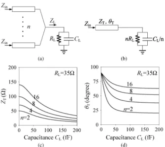
Fig. 1(a) shows the schematic of an ideal -way power com-bining circuit where the output loading is a parallel cir-cuit. With identical (common-mode) input signals, an equiv-alent single-branch configuration can be constructed, as illus-trated in Fig. 1(b). By assuming the line impedance to be and its electrical length , the corresponding input impedance
can be derived as
(1) with
(2) If we treat the power combining circuit as a multi-input single-output impedance transformer that allows the loading
2156-342X © 2014 IEEE. Personal use is permitted, but republication/redistribution requires IEEE permission. See http://www.ieee.org/publications_standards/publications/rights/index.html for more information.
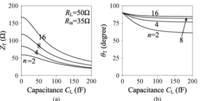
Fig. 1. Capacitive power-combining circuit. (a) In the -way power-com-bining circuit, the loading impedance is made of in parallel with . (b) Equivalent single-branch circuit where is the characteristic impedance of the transmission line and is this line’s electrical length. (c) Optimized for the 2-, 4-, 8-, and 16-way power combining circuits where the loading resistance is fixed at 35 and varies from 0 to 200 fF; the frequency of interest is 94 GHz. (d) The corresponding .
impedance to be replicated at the input ports, i.e., , we then have
(3) (4) Fig. 1(c) and (d) displays the calculated and versus dif-ferent loading capacitance for 2-, 4-, 8-, and 16-way power com-bining circuits where the loading resistance is fixed at 35 and the frequency of interest is 94 GHz. Here we choose 35 rather then 50 is because the output resistance of the 40 1.8 m 65-nm CMOS transistor used in our PA design is close to 35 ; therefore, it will be more convenient using 35 from the beginning of the analysis. In the zero- case, the re-sulting for is the well-known and is 90 . However, if is increased to 80 fF, then and become 26 and 22 , i.e., capacitive output loading allows wider and shorter transmission lines to be used for power-combining pur-pose. It is also interesting to observe that the will remain constant for larger value of .
When compared with the conventional quarter-wavelength resistive power-combining circuit, the shorter and wider trans-mission lines used in the capacitive power combiner means the related power loss can be reduced. Such benefit, however, will be compromised if discernible bandwidth degradation is ob-served. To evaluate the resemblance of to , the deviation parameter in decibels can be defined as
(5) The smaller the , the better the impedance transformation. As shown in Fig. 2(a), the solid curves on the Smith chart are the 77–110 GHz capacitive output loading impedance where
Fig. 2. Frequency response of the two-way capacitive power combining circuit in 77–110 GHz. (a) Impedance displayed on the Smith chart where the solid curves have their fixed at 35 and , 25, 50, and 100 fF, respectively; the dashed curves are the input impedance of the power combiner which is optimized at 94 GHz. (b) Deviation of from . (c) Solid curve is for and fF; the dashed curve 1 is for of the power combiner with optimized and ; the dashed curve 2 is with changed to 41 and is still the same 22 ; the dashed curve 3 is with and changed to 18 . (d) Corresponding deviation in decibels.
is 35 and is 0, 25, 50, and 100 fF, respectively; the dashed curves are the corresponding input impedance of the two-way power combining circuit with and optimized at 94 GHz. Fig. 2(b) shows the where the perfect impedance transfor-mation at 94 GHz makes , i.e., dB, at that spe-cific frequency point and less than 20 dB elsewhere. Since the capacitive power combining technique is more than capable of covering the whole W-band from the perspective, other than the ideal value can be used to accommodate some layout constraints, as demonstrated in Fig. 2(c). Here the solid curve is the output loading of 35 in parallel with 80 fF ; the dashed curve 1 is the where the line impedance used in the power combiner is the optimized 26 and elec-trical length 22 . Since 26 line (of 13 m line width) is a little too wide to implement in the silicon circuit, we instead choose (of 5 m line width) while keep the same 22 , and the resulting is the dashed curve 2. Surely there is no reason that the cannot be finessed too, and so curve 3 is for and . Fig. 2(d) shows the corresponding , and we can see that the adoption of 41 transmission line is just fine.
Theoretically, the bandwidth constraint of the capacitive power combiner can also be determined by the Bode–Fano criteria, which states
WU et al.: 77–110-GHz 65-nm CMOS POWER AMPLIFIER DESIGN 393
If we assume the in-band reflection is 20 dB, i.e., , and total reflection for out-of-band, then we have
(7) The allowed impedance transformation bandwidth will be 77.5 GHz, which is much larger than GHz.
From the DC perspective, since the output power-combining circuit is often used for drain-bias purpose too in most power amplifier design, short and low-impedance microstrip lines means the DC voltage drop can be reduced and thus more efficient operation of the amplifier is expected. In terms of RF, the millimeter-wave power loss is surely proportional to the line’s physical length while its dependence on linewidth is less critical. For a transmission line of physical length
, both its characteristic impedance and propagation constant can be derived from the matrix as [17]
(8) therefore,
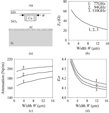
(9) (10) Fig. 3(a) illustrates the profile of the 65-nm CMOS transmis-sion line where the top metal is made of thick copper while the bottom metal is a thin aluminum sheet. Fig. 3(b) is the charac-teristic impedance calculated at 77, 94, and 110 GHz, respec-tively, and they all render the same result. Fig. 3(c) is the simu-lated attenuation constant and here we have taken into account the metal, dielectric, and radiation losses. Among the three loss factors, the metal loss dominates while the radiation loss is very small and can be neglected. If we further split the metal loss into the top-metal loss and the bottom-metal loss, then it is found that the top-metal loss decreases with wider linewidth while, due to more concentrated current density along the bottom metal, the bottom-metal loss increases with wider linewidth. As a re-sult, the attenuation constant reveals a very weak dependence on linewidth in this frequency range. Fig. 3(d) shows the effec-tive relaeffec-tive dielectric constant which is defined as
(11) where is the free-space wavelength.
Fig. 4(a) is the schematic of the cascaded two-way power combining circuit. The total power loss (in dB) along the transmission-lines can be calculated as
(12) Fig. 4(b) shows the simulated results where the solid curve
cor-responds to and , which is used for
loading impedance equal to 35 in parallel with 80 fF;
the dashed curve is with and
Fig. 3. Property of the transmission line used in the power combining circuit. (a) Profile of the 65-nm CMOS transmission line where the top metal is made of copper with conductivity , while the bottom metal sheet is aluminum with . Loss tangent for silicon nitride and silicon oxide used in the simulation are 0.008; the conductivity of silicon substrate is . (b) Simulated characteristic impedance of the transmission line which is independent of frequency. (c) 77, 94, and 110 GHz attenuation constant versus linewidth . (d) Effective relative dielectric constant.
, and is used for . Apparently, power loss of the capacitive power-combining circuit is about 1 dB less than that of the conventional quarter-wave power-combining circuit. Fig. 4(c) and (d) shows the schematic and the simulated results of the direct four-way power-combining circuit and, again, the capacitive combining approach presents a smaller power loss. Though there is a strong incentive in the resistive power-com-bining case to use direct four-way than cascaded two-way, as the former requires a 90 electrical length while the latter demands , there is no such preference in the capacitive power-combining situation.
Finally, we would like to inquire whether other loading arrangements, such as series , parallel , or series , can render similar results. For series loading
with , the characteristic impedance and
electrical length of the transmission line are
(13)
For parallel loading with ,
Fig. 4. Cascaded two-way and direct four-way power combining circuits. (a) Schematic of the cascaded two-way power combiner. (b) Total power loss of the cascaded two-way’s. The solid curve corresponds to transmission line with and , which is used for output loading of and fF. The dashed curve is with and , and is used for and . (c) Schematic of the direct four-way combiner. (d) The corresponding power loss where the solid curve is for and fF, while the dashed curve is for
and .
and
(14) While for series loading with , there is
(15) Fig. 5(a) and (b) shows the and used in the two-way power combining circuit with parallel and series load-ings. For small capacitor, say, smaller than 40 fF, the transmission-line impedance used for series loading is just too large; as increases, the corresponding electrical length will increase and soon surpass that used in the parallel case. Fig. 5(c) and (d) shows the parallel and series loadings: the larger-than-quarter-wavelength transmission line deems both unrealistic. It then becomes clear that the parallel is the preferred loading of choice for power-combining circuit design.
III. 77–110 GHz POWERAMPLIFIERDESIGN
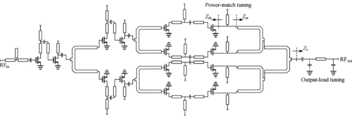
This power amplifier is designated to operate in the linear, i.e., class-A, region, with three amplification stages, where each stage is made of two common-source transistors so that flat gain response can be obtained in 77–110 GHz. In the simulation, wideband input matching is made possible by fine-tuning the input transistors’ loading impedance. Four common-source transistors are arranged, using the aforementioned combining
Fig. 5. Characteristic impedance and electrical length of the transmission line used in power combining circuit with different loading conditions. (a) Theoret-ical where the solid curve is for parallel loading while the dashed curve is for series loading. Here is fixed at 35 and the frequency is 94 GHz. (b) for parallel and series loadings. (c) Theoretical where the solid curve is for parallel loading while the dashed curve is for series loading. (d) Corresponding .
technique, to deliver the power simultaneously. To ensure suf-ficient power gain at 110 GHz, each transistor is made of two paralleled 20 1.8 m ones, i.e., m, with the corresponding reaching 200 GHz [18]; at 1.2 V drain bias voltage, the transistor’s current density is 34 mA/72 m and its output resistance will be close to 35 in 77–110 GHz. Since it is the current swing rather than voltage swing that tends to constrain the circuit’s performance in this low impedance situation, the maximum output power can be determined through conjugate impedance matching. Fig. 6 is the schematic of the 77–110 GHz power amplifier where the output impedance of the final-stage transistors in this frequency range can be modelled as a paralleled circuit with and fF. For efficient power delivery over such wide bandwidth, the capacitive power-combining technique and two additional tuning circuits are employed here. The output-load tuning circuit converts the nominal 50 system impedance into a shunt , with and
fF, to be used as the power combiner’s loading impedance . The two-stage capacitive power-combining circuit, with and , then makes its to be close to , which happens to be . The power-match tuning circuit transforms to its complex-conjugate counterpart
, thus facilitates maximum power extraction from the transistors.
Fig. 7(a) and (b) shows the schematic and simulated results of the output-load tuning circuit. Due to the existence of the pad capacitor , the output impedance presented to this amplifier is not a pure 50 but rather resembles that of point on the Smith chart. At 94 GHz, the series inductor or a short transmission line will transform to . The parasitic shunt capacitance of the DC-blocking capacitor, , then
WU et al.: 77–110-GHz 65-nm CMOS POWER AMPLIFIER DESIGN 395
Fig. 6. Schematic of the 77–110 GHz power amplifier. The output-load tuning circuit will transform the 50 system impedance to paralleled loading, thus facilitates the use of capacitive power-combining network. The power-match tuning circuit allows efficient wideband power extraction from the output transistors.
Fig. 7. Output-load tuning circuit. (a) Schematic where is the para-sitic capacitance of the large DC-blocking capacitor.(b) The solid curve 1 is the intended tracking contour that moves from the origin of the Smith chart to point and then , and finally to , with fF,
pH, and fF. Dashed curve 2 is with zero- , being a quarter-wave transmission line, and a large . Dashed curve 3 has large
, short transmission line, and zero- .
moves to the intended , which has the impedance of 35 in parallel with 80 fF. The solid curve 1 corresponds this tuning process. If zero- is allowed, an assumption that holds true only theoretically in the CMOS but is feasible in GaAs or InP processes, then a quarter-wave transmission line can be employed to transform the 50 to the intended 35 ; a of 80 fF can then be added to reach , as indicated by the dashed curve 2. On the other hand, if the DC-blocking capacitor can be completely removed, then a slightly larger followed by a short could also convert the nominal 50 loading to , as illustrated by the dashed curve 3. Of the three approaches, the used in curve 3 has the smallest value and therefore is the most preferred one from the power conservation perspective; however, the omission of on-chip DC-blocking capacitor may cause problems or other inconve-niences. The zero- approach of curve 2, though simple in analysis, is lossy since it requires a quarter-wave transmission line. By contrast, our tuning method of curve 1 is the most feasible one, as both DC-blocking capacitance and RF pad capacitance have been taken into account. Fig. 8(a) and (b) is the schematic and simulated results of the power-match tuning circuit, which is located between the output transistors and the power combiner. The cascaded two-way power combiner will convert to . The shunt inductor then moves to , which is close to , thus allows efficient power extrac-tion. For better illustration, the , , and contours
Fig. 8. Power-match tuning circuit. (a) Schematic. (b) The 77–110 GHz will be transformed by the two-stage power-combining network into where the total electrical length equal to . The shunt inductor
pH then converts to , which is close to the complex conjugate of the transistor’s output impedance, i.e. .
at 77–110 GHz are all displayed on the Smith chart and it is clear that this tuning circuit is up to the task. As for the loss of the output network, it can be obtained through EM simulation. At 94 GHz, the shunt stub accounts for 0.6 dB power loss, the cascaded 2-way power combiner has dB loss, the DC-blocking contributes 0.3 dB loss and the final tuning line takes away another 0.3 dB; therefore, the total output-network loss is 1.8 dB.
Surely we would like to ask whether there is a more direct way for complex-conjugate power match, or is it possible to have of the power combiner to be the negative value of so that the additional shunt stub can be omitted, and
the answer is yes. In the case of and
, then the impedance and electrical length of the transmission line in the n-way power combiner can be determined as
(16)
and . Now if we have and
, these calculated results are displayed in Fig. 9. For a 4-way direct-power-match combiner, as shown in Fig. 10, the transmission line impedance and electrical length are 47 and
Fig. 9. Impedance and electrical length of the power combiner which trans-forms the negative value of to , thus allows direct power match with the transistor’s output.
Fig. 10. Schematic of the 4-way direct-power-match power combiner. Here , and is paralleled RC circuit.
78 , respectively, and that causes at 94 GHz and therefore the shunt stub can be omitted completely. Though ca-pable of direct power match, this combining technique tends to be narrowband or medium-bandwidth at most, as demonstrated in Fig. 11(a). Here is from our proposed capacitive power combining method while is using the direct-power-match combiner; apparently, the contour is closely following over the 77–110 GHz frequency range. Even worst for the di-rect-power-match method is that, for frequency below 75 GHz, its transformed input impedance will be on the lower half of the Smith chart, i.e., capacitive now. A measure of the bandwidth for complex-conjugate power match can also be through the de-viation parameter, which is defined as
(17) and needs to be changed to for capacitive power com-biner. Fig. 11(b) shows the simulated results and it is clear that our proposed capacitive power combiner, as solid curve, allows effective power extraction from the transistor in 77–110 GHz. On the other way, in terms of loss, the direct-power-match com-biner has 1.8 dB loss at 94 GHz. If we further include the addi-tional 0.2 dB loss from the quarter-wavelength shunt stub used for drain bias, the total loss will approach 2 dB at 94 GHz, which is slightly larger than the 1.8 dB obtained from our proposed method.
Fig. 12 is the photograph of the 77–110 GHz power ampli-fier using 65-nm CMOS process where the chip size is 950 600 m . Since metal–insulator–metal (MIM) capacitors are not available from the foundry during the time of designing this circuit, we instead use custom-made multilayer interdig-ital metal–oxide–metal (MOM) capacitor, which has its
res-Fig. 11. Comparison of capacitive power combiner with direct-power-match power combiner. (a) is the input impedance of the capacitive power com-biner while comes from the direct-power match combiner. is the com-plex conjugate of the transistor’s output impedance. (b) the solid curve is the deviation of from , while the dashed curve is the deviation of from
.
Fig. 12. Photograph of the 77–110 GHz power amplifier with 65-nm CMOS process. The chip size is 950 600 m . With 1.2 V and 480 mA drain bias, the total power consumption is 576 mW. The capacitors are all custom-made multi-layer MOM capacitors. The two pads, and pads too, on both sides of the chip are internally connected.
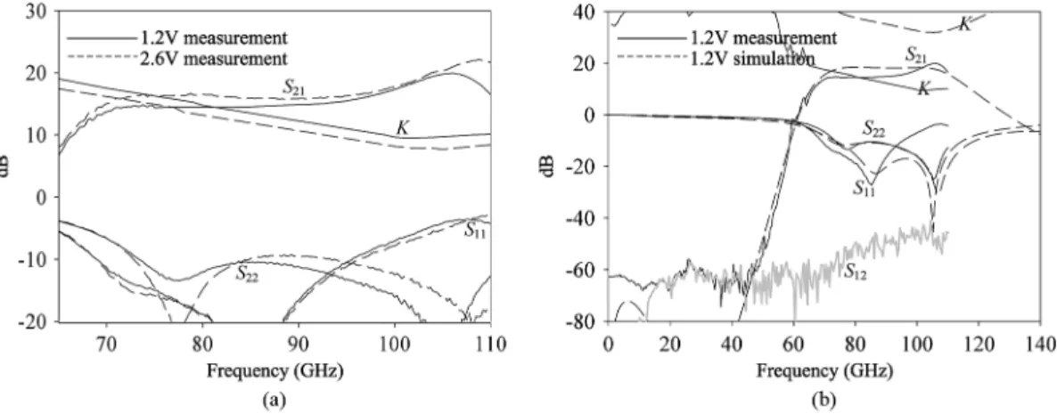
onance frequency well above 120 GHz and thus is valid for use at W-band. With DC bias of 1.2 V and 480 mA, the total power consumption is 576 mW. The W-band -parameters, as measured on-wafer, are displayed in Fig. 13(a) where the solid curves correspond to 1.2 V bias while the dashed curves are with 2.6 V bias; apparently, this amplifier can effectively cover 70–110 GHz from the small-signal perspective and is uncondi-tionally stable, as is judged by the stability factor. The DC-140 GHz -parameters with 1.2 V bias are shown in Fig. 13(b). Due to the limits of the instrument, the measured results are only to 110 GHz while the simulation can be up to 140 GHz. If we decrease the transistor’s gate resistance by 5 , then the peaking toward 110 GHz will be observed in the simulation; this reduction of gate resistance in the modelling can also explain why the measured noise figure is 2 dB lower than its simulated counterpart. As for the large-signal measurement, Fig. 14(a) shows both the measured and simulated output power versus input power at 77 GHz and 110 GHz, which can then be used to derive their respective output-referred 1 dB compression point, or OP1 dB. Fig. 14(b) displays the OP1 dB of 77–110 GHz; due to the constraint imposed by the waveguide port of the power meter, the amplifier’s power performance below 77 GHz has not been measured. In the simulation, the peak of OP1 dB
oc-WU et al.: 77–110-GHz 65-nm CMOS POWER AMPLIFIER DESIGN 397
Fig. 13. -parameters of the power amplifier. (a) The solid curves are measurement with V and mA while the dashed curves are measurement with V and mA. The stability factors are displayed in . (b) DC-140 GHz -parameters and factor in the 1.2 V case where the solid curves are measured results while the dashed curves are their simulated counterparts. The simulated is far below 80 dB and not displayed here. The 3 dB bandwidth for in the simulation covers 70–110 GHz.
Fig. 14. Measured and simulated performance of the power amplifier. (a) Output power versus input power at 77 GHz (black curves) and 110 GHz (gray curves) with bias of V and mA. (b) The output-referred 1 dB compression point from 77 to 110 GHz, as measured with 2 GHz frequency step. The 1 dB bandwidth for OP1 dB is 76–114 GHz in the simulation. (c) 77 GHz (black curves) and 110 GHz (gray curves) output power at different drain bias voltages where the input power is fixed at 0 dBm. (d) Noise figure. In all the plots, the solid curves are the measured results while the dashed curves are their simulated counterparts.
TABLE I
W-BANDSILICON-BASEDPOWERAMPLIFIERCOMPARISON
curs at 87 GHz and it is 11.8 dBm, and the frequency points for
OP1 dB of dBm are 76 and 114 GHz; given
that the 3 dB bandwidth of is 70–110 GHz, it becomes ap-propriate characterizing this PA as 77–110 GHz. Surely, by in-creasing the drain bias voltage , the available output power of this PA can be steadily boosted, as is demonstrated in Fig. 14(c); with 0 dBm input power at 110 GHz, the corresponding output will increase from 13 to 18 dBm when the bias is changed from 1.2 to 2.5 V. Fig. 14(d) is the noise figure of this amplifier where
the measurement is 2 dB lower than the simulation, and this may be coming from the overestimation of the gate resistance in tran-sistor modeling.
A comparison with other CMOS or SiGe power amplifiers covering similar frequency range is tabulated in Table I. It is true that a transformer is capable of pulling more current from the transistors; however, the resulting millimeter-wave PA tends to be of moderate bandwidth, as symmetric circuit layout is dif-ficult to maintain now [12], [21]–[23]. On the other hand, it has
been proposed using a tapered transmission-line in the power combining circuit to obtain wider bandwidth, and the resulting power amplifier can effectively cover 73–97 GHz [24]; how-ever, by using capacitive power combining method, we have demonstrated that an even wider-band PA can be constructed without line tapering. As for the PAE, our 4.5% may not be impressive. This is because, in order to sustain large enough gain across such wide bandwidth, a total of ten transistors has been used for gain amplification while only four are for output power delivery. If lower gain or narrower bandwidth can be ac-cepted or more advanced process such as SiGe is adopted, then the PAE can be increased accordingly.
IV. CONCLUSION
The capacitive power-combining theory has been proposed and analyzed in this paper, which allows a low-loss power-combining network to be constructed over broad bandwidth. A 77–110 GHz power amplifier using 65-nm CMOS process is designed using this technique and then measured on-wafer. It shows an OP1 dB of 12 dBm under 1.2 V bias condiction, and the output power can reach 18 dBm at 2.5 V bias.
ACKNOWLEDGMENT
The authors wish to thank the National Nano-Device Labo-ratories (NDL), Hsinchu, Taiwan, for assistance on chip fabri-cation. Comments and suggestions from the reviewers of this paper are appreciated.
REFERENCES
[1] A. Komijani and A. Hajimiri, “A wideband 77-GHz, 17.5-dBm fully integrated power amplifier in silicon,” IEEE J. Solid-State Circuits, vol. 41, no. 8, pp. 1749–1756, Aug. 2006.
[2] C. Y. Law and A.-V. Pham, “A high-gain 60 GHz power amplifier with 20 dBm output power in 90 nm CMOS,” in IEEE Int. Solid-State Circuits Conf. (ISSCC) Dig. Tech. Papers, 2010, pp. 426–427. [3] M. Bohsali and A. M. Niknejad, “Current combining 60 GHz CMOS
power amplifiers,” in IEEE Radio Freq. Integr. Circuits (RFIC) Symp. Dig. Papers, 2009, pp. 31–34.
[4] B. Martineau, V. Knopik, A. Siligaris, F. Gianesello, and D. Belot, “A 53-to-68 GHz 18 dBm power amplifier with an 8-way combiner in stan-dard 65 nm CMOS,” in IEEE Int. Solid-State Circuits Conf. (ISSCC) Dig. Tech. Papers, 2010, pp. 428–429.
[5] A. Y.-K. Chen, Y. Baeyens, Y.-K. Chen, and J. Lin, “An 83-GHz high-gain SiGe BiCMOS power amplifier using transmission-line current-combining technique,” IEEE Trans. Microw. Theory Techn., vol. 61, no. 4, pp. 1557–1569, Apr. 2013.
[6] W. Tai, L. R. Carley, and D. S. Ricketts, “A 0.7 W fully integrated 42 GHz power amplifier with 10 percent PAE in 0.13 m SiGe BiCMOS,” in IEEE Int. Solid-State Circuits Conf. (ISSCC) Dig. Tech. Papers, Feb. 2013, pp. 142–143.
[7] D. Chowdhury, P. Reynaert, and A. M. Niknejad, “A 60 GHz 1 V 12.3 dBm transformer-coupled wideband PA in 90 nm CMOS,” in IEEE Int. Solid-State Circuits Conf. (ISSCC) Dig. Tech. Papers, 2008, pp. 560–635.
[8] T. LaRocca, J. Y.-C. Liu, and M.-C. F. Chang, “60 GHz CMOS am-plifiers using transformer- coupling and artificial dielectric differential transmission lines for compact design,” IEEE J. Solid-State Circuits, vol. 44, no. 5, pp. 1425–1435, May 2009.
[9] I. Aoki, S. D. Kee, D. B. Rutledge, and A. Hajimiri, “Fully integrated CMOS power amplifier design using the distributed active-transformer architecture,” IEEE J. Solid-State Circuits, vol. 37, no. 3, pp. 371–383, Mar. 2002.
[10] K. H. An, O. Lee, H. Kim, D. H. Lee, J. Han, K. S. Yang, Y. Kim, J. J. Chang, W. Woo, C.-H. Lee, H. Kim, and J. Laskar, “Power-combining transformer techniques for fully-integrated CMOS power amplifiers,” IEEE J. Solid-State Circuits, vol. 43, no. 5, pp. 1064–1074, May 2008. [11] J.-W. Lai and A. Valdes-Garcia, “A 1 V 17.9 dBm 60 GHz power am-plifier in standard 65 nm CMOS,” in IEEE Int. Solid-State Circuits Conf. (ISSCC) Dig. Tech. Papers, 2010, pp. 424–425.
[12] K.-Y. Wang, T.-Y. Chang, and C.-K. Wang, “A 1 V 19.3 dBm 79 GHz power amplifier in 65 nm CMOS,” in IEEE Int. Solid-State Circuits Conf. (ISSCC) Dig. Tech. Papers, 2012, pp. 260–262.
[13] S. Aloui, Y. Luque, N. Demirel, R. Plana, D. Belot, and E. Kerherve, “Optimized power combining technique to design a 20 dB gain, 13.5 dBm OCP1 60 GHz power amplifier using 65 nm CMOS technology,” in IEEE Radio Freq. Integr. Circuits (RFIC) Symp. Dig. Papers, 2012, pp. 53–56.
[14] A. Natarajan, A. Komijani, X. Guan, A. Babakhani, and A. Hajimiri, “A 77-GHz phased-array transceiver with on-chip antennas in silicon: Transmitter and local LO-path phase shifting,” IEEE J. Solid-State Cir-cuits, vol. 41, no. 12, pp. 2807–2819, Dec. 2006.
[15] A. Valdes-Garcia, S. T. Nicolson, J.-W. Lai, A. Natarajan, P.-Y. Chen, S. K. Reynolds, J.-H. Conan Zhan, D. G. Kam, D. Liu, and B. Floyd, “A fully integrated 16-element phased-array transmitter in SiGe BiCMOS for 60-GHz communications,” IEEE J. Solid-State Circuits, vol. 45, no. 12, pp. 2757–2773, Dec. 2010.
[16] Y. A. Atesal, B. Cetinoneri, M. Chang, R. Alhalabi, and G. M. Rebeiz, “Millimeter-wave wafer-scale silicon BiCMOS power amplifiers using free-space power combining,” IEEE Trans. Microw. Theory Tech., vol. 59, no. 4, pp. 954–965, Jan. 2011.
[17] D. M. Pozar, Microwave Engineering, 4th ed. Hoboken, NJ, USA: Wiley, 2012.
[18] B. Heydari, M. Bohsali, E. Adabi, and A. M. Niknejad, “Millimeter-wave devices and circuit blocks up to 104 GHz in 90 nm CMOS,” IEEE J. Solid-State Circuits, vol. 42, no. 12, pp. 2893–2903, Dec. 2007. [19] J. Kim, H. Dabag, P. Asback, and J. F. Buckwalter, “Q-band and
W-band power amplifiers in 45 nm CMOS SOI,” IEEE Trans. Mi-crowave Theory Tech., vol. 60, no. 6, pp. 1870–1877, June 2012. [20] D. Sandstrom, M. Varonen, M. Karkkainen, and K. Halnen, “W-band
CMOS amplifiers achieving 10 dBm saturated output power and 7.5 dB NF,” IEEE J. Solid-State Circuits, vol. 44, no. 12, pp. 3403–3409, Dec. 2009.
[21] D. Sandstrom, B. Martineau, M. Varonen, M. Karkkainen, A. Cathelin, and K. Halnen, “94 GHz power-combining power amplifier with 13 dBm saturated output power in 65 nm CMOS,” in IEEE Radio Freq. Integr. Circuits Symp. 2011, June 2011, pp. 1–4.
[22] Q. J. Gu, Z. Xu, and M.-C. F. Chang, “Two-way current-combining W-band power amplifier in 65-nm CMOS,” IEEE Trans. Microwave Theory Techn., vol. 60, no. 5, pp. 1365–1374, May 2012.
[23] Y. Zhao and J. R. Long, “A wideband, dual-path, millimeter-wave power amplifier with 20 dBm output power and PAE above 15% in 130 nm SiGe-BiCMOS,” IEEE J. Solid-State Circuits, vol. 47, no. 9, pp. 1981–1997, Sep. 2012.
[24] E. Afshari, H. Bhat, X. Li, and A. Hajimiri, “Electrical funnel: A broad-band signal combining method,” in IEEE Int. Solid-State Circuits Conf. (ISSCC) Dig. Tech. Papers, 2006, pp. 751–760.
Kun-Long Wu was born in Kaohsiung, Taiwan,
R.O.C., in 1987. He received the B.S. degree from the Department of Electrical Engineering, National Sun Yat-Sen University, Kaohsiung, Taiwan, in 2009, the M.S. degree from the Electronics Engi-neering, National Chiao Tung University, Hsinchu, Taiwan, in 2011, and is currently working toward the Ph.D. degree in electrical engineering at the same university. His research interest is in mil-limeter-wave transceiver design.
WU et al.: 77–110-GHz 65-nm CMOS POWER AMPLIFIER DESIGN 399
Kuan-Ting Lai was born in Taichung, Taiwan. She
received the B.S. degree in materials science and engineering from National Cheng Kung University, Tainan, Taiwan, in 2012, and the M.S. degree in electronics engineering from National Chiao Tung University, Hsinchu, Taiwan, in 2014, where she was working on millimeter-wave GaAs and CMOS power amplifier design.
Robert Hu received B.S.E.E. degree from National
Taiwan University, Taipei, Taiwan, in 1990, and the Ph.D. degree from The University of Michigan at Ann Arbor, MI, USA, in 2003.
From 1996 to 2003, he was working in the Academia Sinica, Taipei, Taiwan, on the mil-limeter-wave receivers. He is currently with the Department of Electronics Engineering, National Chiao Tung University, Hsinchu, Taiwan. His research interests include microwave and mil-limeter-wave electronics.
Christina F. Jou was born in Taipei, Taiwan, in
1957. She received the B.S., M.S., and Ph.D. degrees in electrical engineering from the University of California, Los Angeles, CA, USA, in 1980, 1982, and 1987, respectively. The subject of her doctoral thesis was the millimeter-wave monolithic Schottky diode-grid frequency doubler.
From 1987 to 1990, she worked at Hughes Air-craft Company, Torrence, CA, USA as a member of the Technical Staff in the Microwave Products Divi-sion, where she was responsible for microwave de-vice modelling. In 1990, she joined National Chiao Tung University where she is now a Professor. Her current research is in developing microwave/RF active circuits and MEMS devices.
Dow-Chih Niu was born in Taipei, Taiwan, in 1956.
He received the B.S. degree in electro-physics and M.S. degree in electronics engineering from the Na-tional Chiao Tung University in 1978 and 1982, re-spectively, and the Ph.D. degree from UCLA, Los Angeles, CA, USA, in 1993..
From 1982 to 1991, he was with Chung-Shan In-stitute of Science and Technology (CSIST), Hsinchu, Taiwan. He is currently with Chung-Shan Institute of Science and Technology (CSIST), Hsinchu, Taiwan, and is in charge of the development of microwave and millimeter-wave sub-systems.
Yu-Shao Shiao received the B.S. degree in
commu-nications engineering and the M.S. degree in elec-tronics engineering from National Chiao Tung Uni-versity in Taiwan, in 1996 and 1998, respectively. He, later, received the second M.S. degree in physics from National Taiwan University in 2001, and the Ph.D. degree in astronomy from University of Illi-nois at Urbana-Champaign in 2008.
He is currently with National Nano-Device Lab-oratories, Hsinchu, Taiwan. His main research inter-ests include mixed-signal and RF integrated circuit design in CMOS and BiCMOS technology, such as data converters, phase lock loops, and voltage-controlled oscillators. He also works on scientific instrumen-tation in high energy physics and astronomy, including cryogenic detectors and circuits, low noise amplifiers, millimeter and sub-millimeter receivers.