GaN light emitting diodes with V-shaped pits
Chi-Kang Li, Chen-Kuo Wu, Chung-Cheng Hsu, Li-Shuo Lu, Heng Li, Tien-Chang Lu, and Yuh-Renn Wu,
Citation: AIP Advances 6, 055208 (2016); doi: 10.1063/1.4950771 View online: http://dx.doi.org/10.1063/1.4950771
View Table of Contents: http://aip.scitation.org/toc/adv/6/5 Published by the American Institute of Physics
AIP ADVANCES 6, 055208 (2016)
3D numerical modeling of the carrier transport
and radiative efficiency for InGaN/GaN light emitting
diodes with V-shaped pits
Chi-Kang Li,1Chen-Kuo Wu,1Chung-Cheng Hsu,1Li-Shuo Lu,1Heng Li,2
Tien-Chang Lu,2and Yuh-Renn Wu1,a
1Graduate Institute of Photonics and Optoelectronics and Department of Electrical
Engineering, National Taiwan University, Taipei, 10617, Taiwan
2Department of Photonics and Institute of Electro-Optical Engineering, National Chiao-Tung
University, Hsinchu 30050, Taiwan
(Received 27 December 2015; accepted 4 May 2016; published online 11 May 2016)
In this paper, influence of a V-pit embedded inside the multiple quantum wells (MQWs) LED was studied. A fully three-dimensional stress-strain solver and Poisson-drift-diffusion solver are employed to study the current path, where the quantum efficiency and turn-on voltage will be discussed. Our results show that the hole current is not only from top into lateral quantum wells (QWs) but flowing through shallow sidewall QWs and then injecting into the deeper lateral QWs in V-pit structures, where the V-pit geometry provides more percolation length for holes to make the distribution uniform along lateral MQWs. The IQE behavior with different V-pit sizes, threading dislocation densities, and current densities were analyzed. Substantially, the variation of the quantum efficiency for different V-pit sizes is due to the trap-assisted nonradiative recombination, effective QW ratio, and ability of hole injections. C 2016 Author(s). All article content, except where
otherwise noted, is licensed under a Creative Commons Attribution (CC BY) license (http://creativecommons.org/licenses/by/4.0/).[http://dx.doi.org/10.1063/1.4950771]
I. INTRODUCTION
III-nitride optoelectronic devices such as light emitting diodes (LEDs) and laser diodes (LDs) are becoming essential roles to replace the traditional light sources nowadays. Driving LED chips with high current densities is inevitable to extend the market of solid-state lighting for the purpose of lower costs, smaller volumes, and higher illuminations within a single chip. However, the e ffi-ciency is significantly decreased at larger injection current densities, which is called droop effect.1
The limitation is fundamentally lying on the material property and crystal quality. The commercial LEDs are generally grown on sapphire substrates where the huge lattice mismatch between GaN and sapphire substrate will lead to a high density of threading dislocations (TDs).2In addition, the lattice mismatch between GaN and InGaN will induce the piezoelectric field in the InGaN layer and lead to quantum-confined Stark effect (QCSE).3The QCSE separates electron and hole wave-functions which reduces the radiative recombination efficiency, and TDs can act as a carrier leakage path to influence the device reliability as well.4,5Besides, TDs are the nonradiative recombination
centers which trap carriers and reduce the internal quantum efficiency (IQE).
Despite GaN-based blue LEDs with such high dislocation densities (∼108 cm−2), the room
temperature photoluminescence (PL) efficiency can be rather high. This is a very typical case because AlGaInP-based red light LEDs have a low luminescence even with relatively lower dislo-cation densities (more than 103cm−2).6This might be attributed to the carrier localization caused by indium fluctuation that reduces the nonradiative recombination.7–9 Regarding with our recent studies, the indium fluctuation incorporated into the simulation model is exceptionally fitting the
aElectronic mail:yrwu@ntu.edu.tw
experimental L-I-V curves by adopting more reasonable material parameters.10,11 On the other
hand, many researches have been reported that the inverted hexagonal V-shaped pit (V-pit) forma-tion are considered to be induced by TDs,12,13where V-pits might be the key role to improve the device efficiency under such high dislocation densities.14 The studies show that active regions in structures with the V-pit are composed of the normal lateral c-plane quantum wells (QWs) and inclined sidewall [10¯11] facet QWs, where the indium composition of lateral c-plane QWs is higher than that of inclined QWs. The potential energy in sidewall QWs is higher than that in c-plane QWs and behaves as a barrier to avoid carriers diffusing into the TDs, which means that it might screen the nonradiative recombination center to ensure the high efficiency under a high density of TDs.15
Therefore, under certain conditions, V-pits might improve the GaN-based LED performance with a relatively higher density of TDs except that the active recombination area is reduced.
The roles of V-pit structures in the GaN/InGaN LEDs with or without superlattice (SL) layers beneath are already studied.16–18Except for screening the TDs from nonradiative recombination, the better hole injection into lateral QWs is also introduced by the 2D semi-section simulation.19and experimental measurements.20The influence of V-pit diameters on the efficiency is also discussed by PL measurements.21In addition, the atom probe tomography (APT) data indicates that the
struc-ture of QWs in V-pit regions is deformed, where the geometry is adjusted, and the width and indium composition of inclined sidewall QWs in V-pits are especially thinner and lower.22Moreover,
exper-iments demonstrated that the energy barriers between lateral and sidewall QWs are depending on the V-pit diameter and tried to explain the PL radiative efficiency.14However, it is still vague about
how the current path is in the V-pit structure and the trend of PL efficiency with diverse V-pit diameters.21Therefore, in this paper we will construct the fully three-dimensional (3-D) model by assessing the real strain distribution, trap-induced potential pulling, and carrier transport equations to discuss the current path because of the non-planar geometry and current spreading effect.23The quantum efficiency and turn-on voltage behavior will be studied to explain the experimental data as well as the physics behind.
II. SIMULATION METHOD
In this paper, we use the 3-D finite element method (FEM) to solve the stress-strain equations to obtain the strain distribution over the entire V-pit structure.24The calculated strain is transformed to
the piezoelectric polarization field by the following formula
Ppz=*. . . , e15ϵxz, e15ϵyz, e31(ϵxx+ ϵyy) + e33ϵzz, + / / / -(1)
where ϵxx, ϵyy, ϵzzare normal strains, and ϵyz, ϵzx, ϵxyare shear strains. Ppzis the strain-induced
piezoelectric polarization. e15, e31, and e33are piezoelectric coefficients, where the values can be
found in Ref.25, and other terms are zero due to the symmetry of Wurtzite crystal structures. By taking the divergence of the total polarization (Ptotal(r)) in the space including spontaneous
and piezoelectric polarization field, the polarization charge ( ρpol(r)) induced at each mesh grid point
can be calculated. The induced fixed polarization charge at different positions will be implemented into Poisson and drift-diffusion solver to obtain the potential (V(r)) as below,
∇ϵ(r)∇V(r) = n(r) − p(r) + N−A(r) − ND+(r) + ∇ · Ptotal(r), (2) Jn(r) = qµnn(r)∇V (r) + qDn∇n(r), (3) Jp(r) = qµpp(r)∇V (r) − qDp∇p(r), (4) ∇ · Jn, p(r) = q(SRH(r) + B0n(r)p(r) + C0(n2(r)p(r) + n(r)p2(r))), (5) SRH(r) = p(r)n(r) − n 2 i τn(p(r) + nie Ei−Et K BT ) + τp(n(r) + nieEt−EiK BT ) , (6)
055208-3 Li et al. AIP Advances 6, 055208 (2016)
where ϵ(r) is the permittivity. n(r) and p(r) are free electron and hole carriers. N−
A(r) and ND+(r) are
the ionized acceptor and donor density. Jnand Jpare the electron and hole current, respectively. The
nonradiative carrier lifetimes τnand τpare 5.0×10⁻⁸s except for the TD region. B0is the radiative
recombination coefficient and set to 2.0×10⁻¹¹ cm3/s. C
0 is the Auger recombination coefficient
and set to 2.0×10⁻³¹cm6/s. All of above parameters are position dependent and commonly used
to examine droop effects.26,27The TD region is divided into donor-like traps (in p-GaN layer) and
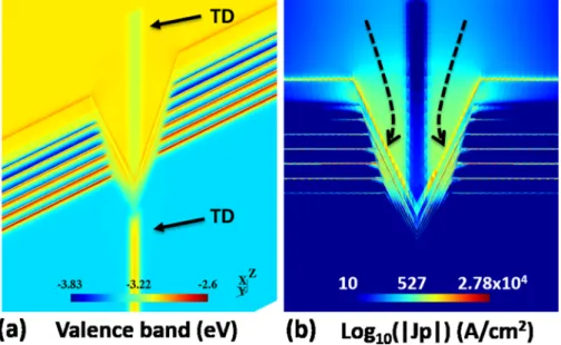
acceptor-like traps (in n-GaN layer) as shown in Fig. 1(a)that are capable of capturing holes and electrons, respectively. The donor-like traps are distributed above the QWs, while the acceptor-like traps are distributed below the QWs, where the density of traps (Nt) is 1.0×1019cm−3. This study
uses the Shockley-Read-Hall (SRH) model to account for the defect or trap assisted nonradia-tive recombination. Et is the energy level for traps, which is assumed at the midgap for both
acceptor-like and donor-like traps. Ei and ni are the intrinsic energy level and intrinsic carrier
density, respectively. τnand τpin TD regions as shown in Fig.1(a)are assumed to be 1.0×10⁻¹²s,
which is quite small and carriers will almost recombine nonradiatively once electrons and holes are flowing into this region.
The details of 3D Poisson and drift-diffusion solver can be referred to our previous publica-tion.28 The simulation structure is shown in Fig. 1(a), where the epi-layers and dimensions are
FIG. 1. (a) Cross-sectional view and detailed dimensions of the simulation structure for the V-pit LED. (b) TEM (provided by prof. Tien-Chang Lu (NCTU)) (c) Calculated polarization charge distribution (cm−3).
suggested by the transmission electron microscopy (TEM) as Fig. 1(b) shows. In addition, the mesh structure is constructed by GMSH program.29 The middle orange line is the location of
TDs that is assumed to be 20 nm width according to TEM and Scanning Transmission Elect-ron Microscope (STEM).15,30There are 6-pairs of InGaN/GaN multiple quantum wells (MQWs),
where the indium compositions of lateral c-plane QWs and sidewall [10¯11] facet QWs are 17% and 7%, respectively.21,22 Besides, the thickness of c-plane QWs is 3 nm that is larger than
side-wall [10¯11] facet QWs with 0.87 nm depending on epi-growth conditions.16 The p-type doping densities in Al0.15Ga0.85N (electron blocking layer (EBL)) and GaN layer are 7.0×1019 cm−3and
2.0×1019cm−3, and the activation energies are 205 meV and 170 meV, respectively. The n-type GaN doping density is 5.0×1018cm−3.
III. RESULTS AND DISCUSSION
This study attempts to understand how the current path influenced by TDs and sizes of the V-pit structure. A series of the V-pit diameter will be studied, including 180 nm, 220 nm, 280 nm, and 340 nm. To simplify the problem and the limitation of current computation memory, we simulate a single V-pit covered by contacts at top and bottom, where the total simulation dimension is 700 nm × 700 nm, which is corresponding to a typical 2.0×108cm−2TD density as a reference case.
Besides, we did not consider the slight variation of indium compositions and well thickness in the sidewall QWs for different V-pit diameters, which might happen in different fabrication processes. At the beginning, the induced polarization charge is verified25,31 and a slight strain relaxation at
the corner is observed. A larger polarization charge is induced in lateral c-plane QWs, and the smaller polarization charge is induced along the [10¯11] sidewall QWs, where the direction of the piezoelectric field is opposite in this semipolar plane as shown in Fig. 1(c), which matches the results of Romanov et.al.25
Figure 2(a) shows the calculated 3-D valence band potential by Poisson and drift-diffusion solver with the calculated strain distribution. In the p-GaN layer, the valence band potential is pulled down by trapping holes along TDs, while in the n-GaN layer, the valence band potential is pulled up due to trapping of electrons.32The trapped holes in the p-GaN layer will expel holes to flow into this region but will attract electrons. Therefore, the hole current are expelled by the pulling potential and diffused into lateral c-plane QWs through the sidewall of V-pits as shown in Fig.2(b). The hole current is not only from top injection into lateral c-plane QWs but also flowing along the inclined
FIG. 2. (a) 3-D valence band potential distribution (eV) by clipping the certain plane off. (b) Distribution of scalar hole current density (A/cm2). The V-pit diameter is 180 nm and the current density is 20 A/cm2.
055208-5 Li et al. AIP Advances 6, 055208 (2016)
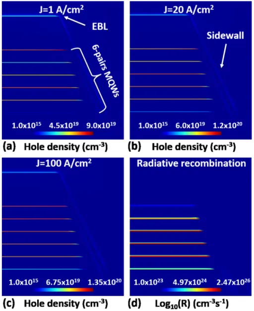
FIG. 3. (a)-(c) are the hole density distribution (cm−3) at 1, 20, and 100 A/cm2. (d) Radiative recombination rate distribution
(cm−3s−1) at 20 A/cm2. The V-pit diameter is 180 nm for all cases.
sidewall QWs due to the lower indium composition and the smaller polarization field (smaller piezoelectric barrier). In conventional planar LEDs, the hole density distribution in different QWs is not uniform, where the hole density is mostly crowded at the top QW (last QW) and is harder to inject into the bottom QW (first QW) due to the low mobility of hole. However, in the V-pit LED, the sidewall QWs provide an additional hole percolation path to make the hole density distribution more uniform in different c-plane QWs as shown in Fig. 3. At low current densities, the hole density distribution is mainly located at the third and last QWs attributed from the top injection and sidewall injection as shown in Fig.3(a). As the current density (applied voltage) increases, the hole density at the third and fourth QWs increases by successive sidewall injections. When the current density approaches 100 A/cm2, the hole density distribution is mainly crowded at last three top QWs
because the applied voltage is large enough to inject holes from top by overcoming c-plane QW barriers induced by piezoelectric fields. By examining the radiative recombination distribution at 20 A/cm2, lateral deeper QWs are the actual active region, where the second to fourth QWs have
stronger radiative recombination rates as shown in Fig.3(d). As a result, the V-pit structure does not only screen TDs, but assists hole injection into the deeper QWs.
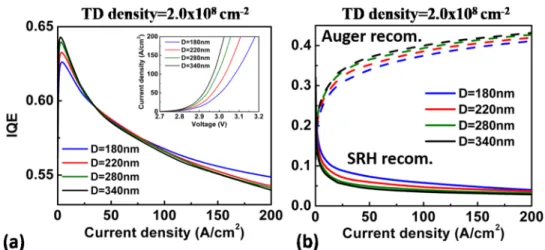
FIG. 4. (a) IQE versus different current densities (A/cm2). The inset of Fig. (a) is the calculated I-V curve. (b) Ratio of SRH
and Auger recombination to the injection current versus different current densities (A/cm2). The TD density is 2.0×108cm−2.
The I-V and IQE curves are calculated as shown in Fig. 4(a) Since a larger V-pit provides an extensive area for carriers injection from the sidewall into c-plane QWs, the turn-on voltage is pushed smaller. Furthermore, the IQE peak value (below 20 A/cm2) is higher for a larger V-pit
diameter. As we know, electrons and holes are mainly trapped at TDs center near the bottom corner of the V-pit due to comparatively lower potentials. In addition, the resistance for electrons and holes is unbalanced, where the hole is more resistive than the electron. For a larger diameter V-pit, the hole current is hard to achieve the bottom of the sidewall QWs due to high resistances of the p-GaN layer and has a widespread percolation path with a large cross-sectional sidewall area. Hence, the nonradiative recombination is weaker at the bottom of sidewall QWs for a larger V-pit diameter as shown in Figs.5(a) and5(b). When the V-pit diameter further increases to 340 nm, the increas-ing peak IQE value is saturated because the SRH nonradiative recombination is not continued to decrease as shown in Fig.4(b). As a result, we could conclude that the nonradiative recombination along TDs will limit the IQE peak value at a lower current density. In our simulation, the IQE peak value is lower compared with the commercial LEDs33,34due to the ABC coefficients we used for the
FIG. 5. (a) and (b) are the nonradiative recombination rate distributions (cm−3s−1) for the 180 nm and 340 nm V-pit diameters,
055208-7 Li et al. AIP Advances 6, 055208 (2016)
simulation.27,35,36In addition to ABC coefficients, the nonradiative recombination in the TD region
and reduced quantum well area will further decrease the IQE peak value. The influence of parameter setting will be discussed in the later section.
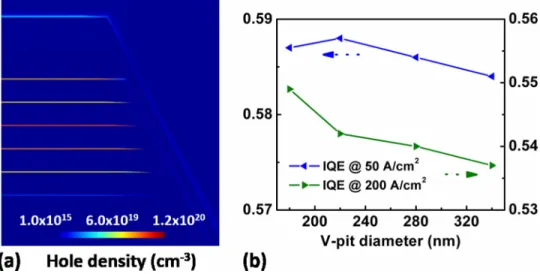
As the current density increases, the Auger recombination starts to affect the system as shown in Fig.4(b). The Auger recombination continues to be enhanced with a smaller effective QW ratio (ratio of lateral c-plane QW areas to the total dimension) by expanding the V-pit size to accumulate high carrier densities in c-plane QWs. The effective QW ratio is smaller when the V-pit diameter becomes larger due to the fixed in-plane area. In other words, the volume of lateral QWs is smaller for a larger V-pit diameter to accommodate carriers, which induces relatively high carrier densi-ties inside QWs as shown in Fig. 6(a)compared with Fig.3(b)to enhance Auger recombination. Therefore, the droop effect happens earlier and more significant for a larger V-pit size as shown in the green line of Fig.6(b). Meanwhile, when the V-pit diameter increases beyond the hole current spreading length (vertical path) to avoid it extending to the bottom of sidewall QWs, the nonradia-tive recombination in TDs does not continue to decrease for the V-pit diameter above 280 nm and the Auger recombination continues to increase due to smaller active volume size. As a result, we also found that the IQE curve among various V-pit diameters exhibits a switched behavior as shown in the blue line of Fig.6(b), which has a good agreement with the experiments.14,21
With regard to the irregular distribution of TDs in the real epi-layers, the TD density we used is an averaging number. To discuss the influence of TD densities for the overall LED performance, we further simulated 1.0×108cm−2and 6.25×108cm−2TD densities, which are corresponding to
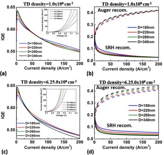
1 µm × 1 µm and 700 nm × 700 nm simulation area, respectively. Figures 7(a)and7(c)show the computed I-V and IQE curve for various V-pit diameters. It is clearly observed that the droop effect is more obvious with a higher TD density due to the inherent smaller effective QW ratio for large V-pit sizes. The IQE curve for various V-pit diameters is crossed at a smaller current density when the TD density is larger. Besides, the switched IQE behavior is observed in terms of higher (6.25×108cm−2) or lower (1.0×108cm−2) TD densities.
At 1.0×108cm−2TD density, because the entire c-plane QW region is wider compared to the
TD size where the influence of TDs becomes smaller, the SRH nonradiative recombination would stop to affect the IQE at larger V-pit diameters. In addition, the effective QW ratio does not change too much by varying V-pit sizes to trigger off the Auger recombination as shown in Fig. 7(b). Therefore, we could know that the TD density is a factor as well to impact the variation of IQE behavior for various V-pit diameters, where the IQE behavior is depending on the Auger recombina-tion and SRH nonradiative recombinarecombina-tion that are modulated by TD densities. Moreover, the current injection from V-pit sidewalls is more unhindered for a smaller simulation dimension at which the V-pit occupies a large portion making the turn-on voltage smaller with a high density of TDs.
FIG. 6. (a) Hole density distribution (cm−3) of a 340 nm V-pit diameter at 20 A/cm2. (b) IQE values at certain current
FIG. 7. (a) and (c) are the IQE versus different current densities (A/cm2) for the 1.0×108cm−2and 6.25×108cm−2TD
densities, respectively. The inset of Figs. (a) and (c) are the calculated I-V curves. (b) and (d) are the ratio of SRH and Auger recombination to the injection current versus different current densities (A/cm2) for the 1.0×108cm−2and 6.25×108cm−2
TD densities, respectively.
In addition to the TD density, we also examine the dependence between the IQE curve and ABC coefficients. We consider the 180 nm V-pit diameter and 2.0×108 cm−2 TD density as the
reference case. As shown in Fig.8(a), when we increase the nonradiative carrier lifetime in the TD region to decrease the SRH recombination, the peak IQE value increases as expected. Besides, if
FIG. 8. (a) IQE curve with various nonradiative carrier lifetimes. τ is the nonradiative carrier lifetime except for the TD region and τTDis the nonradiative carrier lifetime of the TD region, where nonradiative electron and hole lifetimes are the
same. (b) IQE curve with various radiative recombination coefficients (B0) and Auger recombination coefficients (C0). C0is
055208-9 Li et al. AIP Advances 6, 055208 (2016)
the nonradiative carrier lifetime except the TD region becomes large as shown in the black line of Fig.8(a), the peak IQE value increases as well. Therefore, the SRH recombination dominates in the lower current density region, which is the first power dependence on the carrier concentration. On the other hand, when we enhance the radiative recombination coefficient from 2.0×10⁻¹¹cm3/s
to 7.0×10⁻¹¹cm3/s, the overall IQE increases and the droop effect is slightly diminished as shown
in Fig. 8(b). In addition, the increase of Auger coefficients does not only deteriorate the overall IQE, but significantly increase the droop effect. As a result, we could conclude that the radiative recombination and Auger recombination dominate the IQE as the current density increases, which indicate the second and third power dependence on the carrier concentration, respectively.
IV. CONCLUSION
In conclusion, this study presents a 3-D numerical analysis to investigate the current path in the V-pit LED. By examining the effect of TDs in the V-pit structure, we found the potential is pulled by the activation of traps and expel carriers from TD regions to diffuse into sidewall QWs without significant nonradiative recombination. The simulation results also shows the current is flowing through shallow sidewall QWs and then injecting into the deeper c-plane QWs, where the V-pit geometry provides more percolation length for holes to make the hole distribution uniform through c-plane MQWs. Theoretically, the IQE curve with various V-pit diameters is determined by the nonradiative recombination along TDs, effective QW ratio, and hole distribution along c-plane QWs. The peak IQE value is limited by nonradiative recombination along TDs at lower current densities. It is higher as the V-pit diameter is larger because holes have higher chance to flow into c-plane QWs instead of flowing into the corner of V-pit QWs. However, as the V-pit diameter becomes large enough, it would increase the Auger recombination due to a smaller effective QW ratio. The droop effects will become stronger and happen earlier. According to the experimental PL efficiency measurements,14,21the trend of quantum efficiencies by increasing the V-pit diameter is
not unified, which could be explained by the diameter-dependent energy barrier and effective QW ratio. However, in addition to the effective QW ratio, the hole current path in the nonplanar V-pit geometry influenced by applied voltages is another critical factor to explain the switched behavior. Furthermore, we try to examine various TD densities, where the IQE curve is also correlated with the TD density that a higher TD density induces larger Auger recombination due to the inherent smaller effective QW ratio. The droop effect is very serious for the oversized V-pit that would not be an optimized option among all of simulated TD densities.
This work is supported by Ministry of Science and Technology in Taiwan for the finan-cial support, under Grant Nos. MOST 102-2221-E-002-194-MY3, MOST 104-3113-E-155-001, MOST 104-2923-E-002-004-MY3, and the financial support from project of aim for top university 104R890957.
1J. Iveland, L. Martinelli, J. Peretti, J. S. Speck, and C. Weisbuch,Phys. Rev. Lett.110, 177406 (2013). 2S. Mathis, A. Romanov, L. Chen, G. Beltz, W. Pompe, and J. Speck,J. Cryst. Growth231, 371 (2001).
3O. Ambacher, R. Dimitrov, M. Stutzmann, B. E. Foutz, M. J. Murphy, J. A. Smart, J. R. Shealy, N. G. Weimann, K. Chu,
M. Chumbes, B. Green, A. J. Sierakowski, W. J. Schaff, and L. F. Eastman,Phys. Status Solidi B216, 381 (1999).
4L. C. Le, D. G. Zhao, D. S. Jiang, L. Li, L. L. Wu, P. Chen, Z. S. Liu, Z. C. Li, Y. M. Fan, J. J. Zhu, H. Wang, S. M. Zhang,
and H. Yang,Appl. Phys. Lett.101, 252110 (2012).
5J. Kim, J. Kim, Y. Tak, S. Chae, J.-Y. Kim, and Y. Park,IEEE Electron Device Lett.34, 1409 (2013). 6S. Lester, F. Ponce, M. Craford, and D. Steigerwald,Appl. Phys. Lett.66, 1249 (1995).
7S. Chichibu, T. Azuhata, T. Sota, and S. Nakamura,Appl. Phys. Lett.69, 4188 (1996). 8A. David and M. J. Grundmann,Appl. Phys. Lett.96, 103504 (2010).
9D. Watson-Parris, M. J. Godfrey, P. Dawson, R. A. Oliver, M. J. Galtrey, M. J. Kappers, and C. J. Humphreys,Phys. Rev. B
83, 115321 (2011).
10Y.-R. Wu, R. Shivaraman, K.-C. Wang, and J. S. Speck,Appl. Phys. Lett.101, 083505 (2012). 11T.-J. Yang, R. Shivaraman, J. S. Speck, and Y.-R. Wu,J. Appl. Phys.116, 113104 (2014). 12M. Shiojiri, C. Chuo, J. Hsu, J. Yang, and H. Saijo,J. Appl. Phys.99, 073505 (2006).
13H.-L. Tsai, T.-Y. Wang, J.-R. Yang, C.-C. Chuo, J.-T. Hsu, Z.-C. Feng, and M. Shiojiri,Mater. Trans.48, 894 (2007). 14N. Okada, H. Kashihara, K. Sugimoto, Y. Yamada, and K. Tadatomo,J. Appl. Phys.117, 025708 (2015).
15A. Hangleiter, F. Hitzel, C. Netzel, D. Fuhrmann, U. Rossow, G. Ade, and P. Hinze,Phys. Rev. Lett.95, 127402 (2005). 16S.-H. Han, D.-Y. Lee, H.-W. Shim, J. W. Lee, D.-J. Kim, S. Yoon, Y. S. Kim, and S.-T. Kim,Appl. Phys. Lett.102, 251123
17J. Kim, Y.-H. Cho, D.-S. Ko, X.-S. Li, J.-Y. Won, E. Lee, S.-H. Park, J.-Y. Kim, and S. Kim,Opt. Express22, A857 (2014). 18Z. Quan, J. Liu, F. Fang, G. Wang, and F. Jiang,J. Appl. Phys.118, 193102 (2015).
19Z. Quan, L. Wang, C. Zheng, J. Liu, and F. Jiang,J. Appl. Phys.116, 183107 (2014). 20X. Wu, J. Liu, and F. Jiang,J. Appl. Phys.118, 164504 (2015).
21C.-Y. Chang, H. Li, Y.-T. Shih, and T.-C. Lu,Appl. Phys. Lett.106, 091104 (2015).
22S. Tomiya, Y. Kanitani, S. Tanaka, T. Ohkubo, and K. Hono,Appl. Phys. Lett.98, 181904 (2011). 23C.-K. Li, H.-C. Yang, T.-C. Hsu, Y.-J. Shen, A.-S. Liu, and Y.-R. Wu,J. Appl. Phys.113, 183104 (2013). 24C.-C Hsu, C.-K. Wu, C.-K. Li, T.-C. Lu, and Y.-R. Wu, in 15th NUSOD (2015).
25A. Romanov, T. Baker, S. Nakamura, and J. Speck,J. Appl. Phys.100 (2006).
26E. Kioupakis, P. Rinke, K. T. Delaney, and C. G. Van de Walle,Appl. Phys. Lett.98, 161107 (2011). 27J. Piprek,Phys. Stat. Sol. (A)207, 2217 (2010).
28C.-K. Wu, C.-K. Li, and Y.-R. Wu,J. Comput. Electron.14, 416 (2015). 29C. Geuzaine and J. F. Remacle,Int. J. Numer. Meth. Eng.79, 1309 (2009).
30X. Wu, J. Liu, Z. Quan, C. Xiong, C. Zheng, J. Zhang, Q. Mao, and F. Jiang,Appl. Phys. Lett.104, 221101 (2014). 31O. Ambacher, J. Majewski, C. Miskys, A. Link, M. Hermann, M. Eickhoff, M. Stutzmann, F. Bernardini, V. Fiorentini, V.
Tilak, B. Schaff, and L. F. Eastman,J. Phys.: Condens. Matter14, 3399 (2002).
32C. Youtsey, L. Romano, R. Molnar, and I. Adesida,Appl. Phys. Lett.74, 3537 (1999). 33D.-S. Shin, D.-P. Han, J.-Y. Oh, and J.-I. Shim,Appl. Phys. Lett.100, 153506 (2012). 34H.-Y. Ryu, H.-S. Kim, and J.-I. Shim,Appl. Phys. Lett.95, 081114 (2009). 35C.-K. Li and Y.-R. Wu,IEEE Trans. Electron Devices59, 400 (2012).