Reduced hole injection barrier for achieving ultralow voltage polymer
space-charge-limited transistor with a high on/off current ratio
Yu-Chiang Chao, Yi-Cheng Lin, Min-Zhi Dai, Hsiao-Wen Zan, and Hsin-Fei Meng
Citation: Applied Physics Letters 95, 203305 (2009); doi: 10.1063/1.3261749
View online: http://dx.doi.org/10.1063/1.3261749
View Table of Contents: http://scitation.aip.org/content/aip/journal/apl/95/20?ver=pdfcov Published by the AIP Publishing
Articles you may be interested in
Polymer space-charge-limited transistor as a solid-state vacuum tube triode Appl. Phys. Lett. 97, 223307 (2010); 10.1063/1.3513334
Low voltage active pressure sensor based on polymer space-charge-limited transistor Appl. Phys. Lett. 95, 253306 (2009); 10.1063/1.3266847
Three-dimensional organic field-effect transistors with high output current and high on-off ratio Appl. Phys. Lett. 94, 103307 (2009); 10.1063/1.3098404
Light-emitting polymer space-charge-limited transistor Appl. Phys. Lett. 93, 223301 (2008); 10.1063/1.3027057 Polymer space-charge-limited transistor
Appl. Phys. Lett. 88, 223510 (2006); 10.1063/1.2207838
This article is copyrighted as indicated in the article. Reuse of AIP content is subject to the terms at: http://scitation.aip.org/termsconditions. Downloaded to IP: 140.113.38.11 On: Wed, 30 Apr 2014 08:24:17
Reduced hole injection barrier for achieving ultralow voltage polymer
space-charge-limited transistor with a high on/off current ratio
Yu-Chiang Chao,1Yi-Cheng Lin,1Min-Zhi Dai,1Hsiao-Wen Zan,2,a兲 and Hsin-Fei Meng1,a兲
1Institute of Physics, National Chiao Tung University, Hsinchu 300, Taiwan
2Department of Photonics and Institute of Electro-Optical Engineering, National Chiao Tung University,
Hsinchu 300, Taiwan
共Received 23 August 2009; accepted 14 October 2009; published online 20 November 2009兲 Vertical polymer space-charge limited transistor 共SCLT兲 operated with an ultralow voltage is demonstrated. The influence of aging effect of the oxygen plasma treated indium tin oxide electrode on the hole injection barrier and on the transistor characteristics is investigated. By reducing the hole injection barrier, the on/off ratio as high as 104is obtained at a collector to emitter voltage as low as ⫺0.84 V. The low operation voltage is crucial to the development of low-power large-area polymer transistor array. Inverter characteristics are also demonstrated by connecting a SCLT with a load resistor. © 2009 American Institute of Physics.关doi:10.1063/1.3261749兴
Reducing the operation voltage of transistors is crucial for the development of integrated circuit or large-area tran-sistor array because low operation voltage gives rise to low power consumption. For complementary metal-oxide-semiconductor technology in very-large-scale integration cir-cuits, low operation voltage is achieved by using advanced and expensive lithography processes. For example, 0.18 m process is required to realize metal-oxide-semiconductor field-effect transistors operated by 1 V.1For large-area appli-cations, reducing transistor operation voltage by upgrading lithography system to scaling down the channel length is not cost effective. Thin-film transistors 共TFTs兲, such as metal-oxide TFTs,2 amorphous silicon TFTs,3 and polycrystalline silicon TFTs,4 require operation voltages higher than 5 V. When organic or polymer transistors are considered for the development of printable, flexible, large-area transistor array, operation voltages are even higher than 10 V.
Using vertical-channel transistor structure with ul-trashort channel length is an alternative approach to reduce the operation voltage. In previous reports, vertical polymer metal-base transistors with various base conformations have been demonstrated to reduce the operation voltage to be less than 10 V.5–8 However, it is important to further reduce the operation voltage to suppress power consumption. Since the vertical channel is a thin polymer semiconductor film sand-wiched by two metals共emitter and collector兲, the thin poly-mer film gives rise to a low channel resistance while the injection barrier from metal to polymer causes large contact resistance at the metal/polymer interface. When the operation voltage across the vertical channel is reduced, the voltage drop at the metal/polymer interface significantly influences device performance. However, no research has been con-ducted to understand the influence of hole injection on the characteristics of vertical transistors. Vertical polymer tran-sistor operated with ultralow voltage is still in need. At the same time, low leakage current and high on/off current ratio are required.
In this work, we focus on voltage reduction while keep-ing on/off current ratio. The vertical transistor we used is space-charge limited transistor共SCLT兲. The basic concept of
SCLT was proposed and verified in our previous reports,8in which, to operate the transistors, 4 to 7 V across the vertical channel are required. In this work, we reduce the hole injec-tion barrier at indium tin oxide共ITO兲/polymer interface. The hole current is enhanced at low voltage. Meanwhile, low electric field suppresses leakage current. The high on/off ra-tio of 104 is obtained at a collector to emitter voltage共V
CE兲 as low as ⫺0.84 V. The characteristics of an inverter fabri-cated by connecting a SCLT with a resistor in series are also demonstrated.
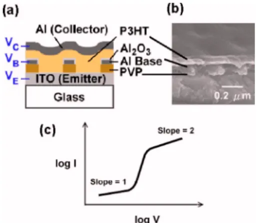
The structure of the SCLT is shown in Fig. 1共a兲. The ITO/poly共3-hexylthiophene兲 共P3HT兲/Al diodes are fabricated on ITO glass substrate with or without O2 plasma treatment on ITO. P3HT of 1200 Å is spin coated from 2.5 wt % chlo-robenzene. To investigate the influence of aging time on the diode characteristics, some ITO glass substrates are stored in glove box for various aging time after O2plasma treatment followed by spin coating P3HT. The plasma chamber is con-nected with glove box such that O2-plasma-treated ITO sub-strates do not contact with ambient air during the investiga-tion of aging time. The SCLT is fabricated on an ITO glass substrate which is flattened by 150 W O2plasma for 30 min. 600 Å cross-linkable poly共4-vinyl phenol兲 共PVP兲 is spin coated on the ITO substrate and then cross-linked at 200 ° C for 60 min in vacuum. Poly共melamine-co-formaldehyde兲
me-a兲Authors to whom correspondence should be addressed. Electronic mail:
[email protected] and [email protected].
FIG. 1. 共Color online兲 共a兲 The schematic device structure of a SCLT. 共b兲 SEM image of device before Al collector deposition. 共c兲 The schematic log I − log V curve of a SCLT. Three regions with different slopes are observed.
APPLIED PHYSICS LETTERS 95, 203305共2009兲
0003-6951/2009/95共20兲/203305/3/$25.00 95, 203305-1 © 2009 American Institute of Physics
This article is copyrighted as indicated in the article. Reuse of AIP content is subject to the terms at: http://scitation.aip.org/termsconditions. Downloaded to IP: 140.113.38.11 On: Wed, 30 Apr 2014 08:24:17
thylated 共Aldrich, Mw⬃511兲 is utilized as a crosslinking agent for PVP. The surface of PVP is turned into hydrophilic by short time exposure of 50 W O2plasma before submerg-ing the substrate into 2000 Å positively charged polystyrene spheres 共Merck, K6–020兲 dilute ethanol solution with 0.8 wt %. The polystyrene spheres are adsorbed on PVP sur-face to serve as the shadow mask. After being submerged in polystyrene spheres solution for 3 min, the substrate is then transferred into a beaker with boiling isopropanol solution for 10 s. The substrate is immediately blown dry to form two dimensional colloidal arrays. 400 Å Al is evaporated as metal base electrode. After removing the polystyrene spheres by an adhesive tape 共Scotch, 3M兲, the PVP at sites without Al coverage is removed by 10 min 150 W O2plasma treat-ment. During the O2plasma treatment, Al2O3is also grown on the Al base. The substrate is then stored in glove box for various time before spin coating P3HT of 1200 Å from 2.5 wt % chlorobenzene. Finally, the Al collector is depos-ited to complete the SCLT with active area as 1 mm2. The scanning electron microscopy共SEM兲 image of device before Al deposition is shown in Fig. 1共b兲. When SCLT is turned on, the relationship between the channel current共IC兲 and the channel voltage 共VCE兲 can be observed by log IC− log VCE curve as shown in Fig.1共c兲. The region with a slope equal to 2 refers that the current is the space-charge limited current. When the slope is equal to 1, the conduction is related to the intrinsic carrier density since hole injection is blocked by the interface barrier.9 Reducing injection barrier is the key to obtaining high current under low voltage.
Hole injection from ITO has been enhanced by many methods including UV/ozone and plasma treatment. In this work, before spin coating P3HT, the surface of ITO emitter is treated with O2 plasma during the plasma etch back pro-cess. As a result, hole injection from ITO to P3HT is im-proved by O2 plasma treatment. The normalized current-voltage curves of ITO/P3HT/Al diodes are shown in Fig.
2共a兲. The normalized current turns on rapidly at low voltage for the diode fabricated on O2-plasma-treated ITO. As for the diode fabricated on ITO without O2 plasma treatment, the normalized current turns on at around 1 V. Previous reports have demonstrated that the changes in surface chemical com-position, surface species and surface carbon contribute to the enhanced ITO work function.10–12 The enhanced ITO work function gives rise to the reduced energy barrier at the inter-face of ITO and P3HT as shown in the inset of Fig.2共a兲. For the diode with low hole injection barrier, hole injection oc-curs at low voltage and hence the turn-on voltage is low. As for the diode with high-injection barrier, high voltage is needed for hole tunneling through the barrier. Since the en-hanced ITO work function is related to the change of surface carbon and surface species, aging effect is expected to sig-nificantly influence ITO work function. As shown in Fig.
2共b兲, aging effect on the O2-plasma-treated ITO is investi-gated. Since 2 min are necessary for transferring sample from plasma chamber into glove box and spin coating P3HT, the minimum aging time is estimated as 2 min. Longer aging time is achieved by store sample in glove box for various period of time. For the diode with 2 min aging time, a rap-idly increasing current is observed when the forward-bias voltage is applied. However, as the aging time increases from 2 to 62 min, the turn-on voltage of ITO/P3HT/Al diode is increased. In the mean time, the contact angle also rises with
the aging time as shown in the inset of Fig.2共b兲. Aging time longer than 62 min causes no apparent change on turn-on voltage and contact angle. The observation can be explained as follow. With the increasing aging time, the surface oxygen concentration decreases and the surface carbon concentration increases, which results in the decrement of ITO work func-tion, and thus increment of hole injection barrier as well as turn-on voltage.13After 62 min aging time, the surface con-dition goes back to that before O2plasma treatment, and the benefit brought by O2plasma treatment disappeared.
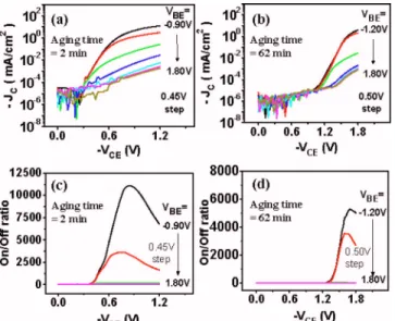
After knowing that O2 plasma treatment decreases the turn-on voltage and enhances the hole current at low voltage while the aging causes the opposite effect, the influence of the O2 plasma treatment and the aging effect on the SCLT characteristics is then investigated. The characteristics of SCLTs made with aging time of 2 min共low-injection-barrier SCLT兲 and 62 min 共high-injection-barrier SCLT兲 are com-pared and shown in Figs. 3共a兲and3共b兲. The VBEis changed from negative to positive to turn on and turn off the SCLT. The off current is reduced by increasing VBE until leakage current occurs and causes a large base current density 共JB兲. Apparently, the collector current density 共JC兲 can be modu-lated by VBE for both SCLT. However, the low-injection-barrier SCLT can be turned on at low voltage 共VCE = −0.3 V兲 but the high-injection-barrier SCLT can only be turned on with higher voltage共VCE= −1 V兲. This agrees with the results obtained form Fig.2. Low-injection-barrier SCLT FIG. 2. 共Color online兲 共a兲 The normalized current-voltage curves of the ITO/P3HT/Al diodes. The ITO surface is treated with or without O2plasma.
The inset shows the schematic energy level diagrams under low and high voltage. The black solid lines represent the Fermi level of ITO with low and high work function. The black dashed line represents the highest occupied molecular orbital of P3HT while device is under low voltage bias. The red dot-dashed line represents the highest occupied molecular orbital of P3HT while device is under high voltage bias.共b兲 The normalized current-voltage curves of the diodes fabricated on ITO substrate with different aging time. Images of water drop on ITO surface with aging time of 2 and 62 min are compared in the inset.
203305-2 Chao et al. Appl. Phys. Lett. 95, 203305共2009兲
This article is copyrighted as indicated in the article. Reuse of AIP content is subject to the terms at: http://scitation.aip.org/termsconditions. Downloaded to IP: 140.113.38.11 On: Wed, 30 Apr 2014 08:24:17
shows good transistor characteristics and the output current density is around 12.7 mA/cm2 as V
CE= −1.2 V. The base current density is in the order of 10−4– 10−3 mA/cm2 and hence the current gain 兩JC/JB兩 is as large as 104 to 105. The on/off ratio for SCLT with low and high injection barrier is plotted as a function of VCE in Figs. 3共c兲 and3共d兲, respec-tively. High on/off ratio of 104 for low-injection-barrier SCLT is obtained at VCE= −0.84 V while that for high-injection-barrier SCLT is about 5000 at VCE= −1.69 V. Even when more negative VCE and VBE are applied on high-injection-barrier SCLT to turn on the emitter-to-collector di-ode, the on/off ratio is still lower than that of low-injection-barrier SCLT. The lower on/off ratio in high-injection-low-injection-barrier SCLT results from higher base-collector voltage drop which increases leakage current and hence reduces the on/off ratio. Operating the SCLT under low voltage can prevent leakage current. Low injection barrier from ITO to P3HT is essential to obtain high output current and high on/off ratio at low operation voltage.
After a SCLT with a high on/off ratio operated within ultralow voltage is fabricated, a resistive-load inverter based on SCLT is demonstrated by connecting a SCLT with a load resistor 共RL= 1 M⍀兲 in series. Schematic inverter cir-cuit is shown in the inset of Fig. 4共a兲. The transfer charac-teristics at various supply voltage 共VDD兲 are shown in Fig.
4共a兲. The output voltage 共Vout兲 can be expressed by Vout =共VDDREC兲/共RL+ REC兲, where RECis the effective resistance from emitter to collector. When input voltage 共Vin兲 applied on base electrode is 1 V共logic “0”兲, the SCLT is in the off state, REC is much larger than RL and the output voltage 共Vout兲 approaches VDD. On the contrary, when Vin is ⫺1 V 共logic “1”兲, the SCLT is in the on state, RECis smaller than
RLand Voutapproaches zero. Ideally, Voutshould be equal to 0 V as the SCLT is in the on state. However, in our case, Vout is not exactly 0 V because RECin the on state is comparable to RL. This problem can be solved by further increasing the on current of SCLT or by replacing RLwith an n-type SCLT. The gain values of the inverter are shown in Fig.4共b兲. The absolute value of voltage gain is 1.4, implying that this de-vice may be used in logic circuits as subsequent stages.14
In summary, the influence of hole injection barrier on the SCLT characteristics is investigated. By fabricating SCLT with minimum aging time after O2 plasma treatment, the minimum hole injection barrier is obtained, the hole current is enhanced at low voltage, and thus the low operation volt-age SCLT is achieved with high on/off ratio of 104at VCEas ⫺0.84 V. The proposed high on/off ratio and low operation voltage SCLT opens a possibility to develop high-performance organic electronics with large-area solution pro-cess. The inverter characteristics represent a promising elec-tronic application with low operation voltage and low power consumption.
This work is supported by the National Science Council of Taiwan under Contract No. NSC97-2628-M-009-016.
1C. W. Kuo, S. L. Wu, S. J. Chang, H. Y. Lin, and Y. P. Wang,J.
Electro-chem. Soc. 155, H611共2008兲.
2A. Suresh and J. F. Muth,Appl. Phys. Lett. 92, 033502共2008兲. 3L. Han, P. Mandlik, K. H. Cherenack, and S. Wagner,Appl. Phys. Lett.
94, 162105共2009兲.
4I. S. Kang, S. H. Han, and S. K. Joo,Appl. Phys. Lett. 91, 222113共2007兲. 5Y. Yang and A. J. Heeger,Nature共London兲 372, 344共1994兲.
6S. H. Li, Z. Xu, G. Yang, L. Ma, and Y. Yang, Appl. Phys. Lett. 93,
213301共2008兲.
7Y. C. Chao, M. H. Xie, M. Z. Dai, H. F. Meng, S. F. Horng, and C. S. Hsu,
Appl. Phys. Lett. 92, 093310共2008兲.
8Y. C. Chao, H. F. Meng, S. F. Horng, and C. S. Hsu,Org. Electron.9, 310
共2008兲.
9Z. Chiguvare and V. Dyakonov,Phys. Rev. B 70, 235207共2004兲. 10D. J. Milliron, I. G. Hill, C. Shen, A. Kahn, and J. Schwartz,J. Appl. Phys.
87, 572共2000兲.
11K. Sugiyama, H. Ishii, Y. Ouchi, and K. Seki, J. Appl. Phys. 87, 295
共2000兲.
12K. H. Lee, H. W. Jang, K. B. Kim, Y. H. Tak, and J. L. Lee,J. Appl. Phys. 95, 586共2004兲.
13J. Y. Deng, Z. Z. You, W. Tao, L. W. Zhi, and J. X. Qiao, Proc. SPIE 6030, 60300G共2006兲.
14M. H. Yoon, H. Yan, A. Facchetti, and T. J. Marks,J. Am. Chem. Soc. 127, 10388共2005兲.
FIG. 3.共Color online兲 The characteristics of SCLTs made with aging time of 共a兲 2 min and 共b兲 62 min. The on/off ratio of SCLTs made with aging time of共c兲 2 min and 共d兲 62 min.
FIG. 4. 共Color online兲 共a兲 Transfer characteristics of the inverter at various
VDD. The schematic inverter circuit is shown in the inset. The load resistance
is 1 M⍀. 共b兲 The corresponding gain values of the inverter.
203305-3 Chao et al. Appl. Phys. Lett. 95, 203305共2009兲
This article is copyrighted as indicated in the article. Reuse of AIP content is subject to the terms at: http://scitation.aip.org/termsconditions. Downloaded to IP: 140.113.38.11 On: Wed, 30 Apr 2014 08:24:17