A Novel Pixel Design for AM-OLED Displays
Using Nanocrystalline Silicon TFTs
Chen-Wei Lin, Mango C.-T. Chao, Member, IEEE, and Yen-Shih Huang
Abstract—This paper presents a novel pixel design for active
matrix organic light emitting diode (AM-OLED) displays using nanocrystalline silicon thin-film transistors (TFTs). The proposed pixel design can effectively reduce the variation of its stored display data caused by the leakage current of nanocrystalline silicon TFTs, which can in turn increase the contrast resolution of AM-OLED displays. With a proper setting of its capacitors, the proposed pixel design can achieve a 5.55 reduction on its display-data variation while requiring only a 1.15 write time when compared to the typical pixel design. The aperture ratio resulting from the layout of the proposed pixel design can also be maintained above 40%, which satisfies the specification of most AM-OLED displays. A series of simulations as well as mea-surement results are provided to validate the effectiveness of the proposed pixel design.
Index Terms—Active Matrix Organic Light Emitting Diode
(AM-OLED), coupling effect, microcrystalline thin-film transistor (TFT), nanocrystalline TFT.
I. INTRODUCTION
D
URING the past few years, major display manufacturers have put a lot research efforts into the area of active ma-trix organic light emitting diode (AM-OLED) displays, which use self-light-emitting devices, require no backlight elements, and in turn are lighter, thinner, and less power-consumed com-pared to the current display mainstream, active matrix liquid crystal display (AM-LCD displays) [1], [2]. AM-OLED display can also provide faster response time, wider viewing angle, and better front-of-screen (FOS) quality, and hence is considered as the best candidate for next-generation displays [1], [2]. In order to build a robust backplane which can reliably control OLED’s current and thus its lightness, a stable and high-quality thin-film transistor (TFT) technology is required. However, the available TFT technologies in current industry are not yet cost-effective or stable enough, which has been the biggest barrier for devel-oping quality AM-OLED displays today [1], [3].Table I compares the three major prospects of the TFT tech-nology used for building the backplane of AM-OLED displays, which are: 1) amorphous silicon ( -Si) TFT; 2) polycrystalline silicon (poly-Si) TFT; and 3) nanocrystalline silicon (nc-Si) TFT (or microcrystalline silicon TFT). The first prospect -Si Manuscript received September 16, 2009; revised December 23, 2009. First published March 11, 2010; current version published May 25, 2011.
C.-W. Lin and M. C.-T. Chao are with the Department of Electronics Engineering and Institute of Electronics, National Chiao Tung Univer-sity, Hsinchu 30010, Taiwan (e-mail: [email protected]; mango@ faculty.nctu.edu.tw).
Y.-S. Huang is with the Industrial Technology Research Institute, 310 Taiwan (e-mail: [email protected]).
Digital Object Identifier 10.1109/TVLSI.2010.2042735
TABLE I
COMPARISON OFSILICON-BASEDTFTS
TFT, which is currently used for building the backplane of AM-LCD displays, has the advantages of low leakage, low process temperature, better electric uniformity, and easy depo-sition, resulting a relatively low manufacturing cost [1], [2], [4]. However, -Si TFT suffers from its low mobility, which may result in a low aperture ratio and in turn low illumination effi-ciency. -Si TFT also suffers from its large threshold-voltage shift over time, which significantly reduces the reliability of AM-OLED displays since a large current needs to pass through the TFTs which drive the OLEDs. Such an OLED-driving TFT is not required in AM-LCD displays, whose light source comes from a stable backlight element.
In contrast with -Si TFT, the second prospect poly-Si TFT, which is also a mature technology in current industry, can pro-vide stable threshold voltage over time and high mobility for driving OLED due to its larger silicon grain size [1], [2]. How-ever, by using the technique of excimer laser annealing for crys-tallization, poly-Si TFT has the disadvantages of low electric uniformity, which limits the application of poly-Si TFT only on small-size panels [1], [2]. Also, the overall manufacturing cost of poly-Si TFT is high because of its high process complexity, the required laser equipments, and its high process temperature. The third prospect nc-Si TFT, whose silicon grain size is between the other two TFT technologies, can overcome the drawbacks of low mobility and poor reliability when compared to -Si TFT, and at the same time overcome the drawbacks of high manufacturing cost and poor electric uniformity when compared to poly-Si TFT. As in [1], [4]–[6], nc-Si TFT can be manufactured by using the conventional 13.56 MHz plasma-enhanced chemical vapor deposition (PECVD), whose manufacturing infrastructures are already well established in current industry for -Si TFT technologies. Furthermore, if the nc-Si TFT is constructed by using the bottom-gate structure [1], [3] instead of the top-gate structure [5], [6], the process flow can match the one used for the current manufacturing of AM-LCD displays. In this condition, the technology of nc-Si TFT can reuse the current production lines of AM-LCD displays and, thus, can be brought to mass production sooner and more economically.
Overall, the nc-Si TFT combines several advantages of both poly-Si and -Si TFTs, is cost-effective in manufacturing, and hence emerges as a promising TFT technology for AM-OLED displays. However, the biggest barrier preventing the nc-Si TFT from production is its high drain-source turn-off current (leakage current). When the typical pixel design is used, this high leakage current may result in either a low contrast resolu-tion or the lose of a stored display data before an image frame is refreshed. A high leakage current is a common drawback of using the PECVD [1], [5] and may become worse when the bottom-gate structure is used [1], [3], [5]. Several previous works attempted to reduce this leakage current from the aspects of changing TFT’s structures [5], [6], material [1], or deposi-tion mechanisms [7], but yet the current progress along this research line is still not sufficient enough to reach the standard for production.
In this paper, we attempt to push the use of nc-Si TFTs into production by proposing a novel pixel design of AM-OLED dis-plays. The proposed pixel design can effectively reduce the de-gree of display-data variation caused by nc-Si TFT’s leakage. Also, its write-time overhead and area overhead can be properly limited by the choice of its capacitance setting and layout tech-niques, respectively. The analysis and simulation for both dis-play-data variation and data write time will then be provided. An optimal configuration of the proposed pixel design can be ob-tained through proper simulation. The measurement result based on a nc-Si TFT technology developed by ITRI [8] further con-firms our analysis and simulation for the proposed pixel design. In general, the contrast resolution saved by the proposed pixel design can be up to more 2 digital bits, which significantly ease the pressure of finding a new low-leakage material or deposition mechanism, and in turn speed up the production of AM-OLED displays using nc-Si TFTs.
II. BACKGROUND OFAM-OLED DISPLAYS AND THETYPICALPIXELDESIGN
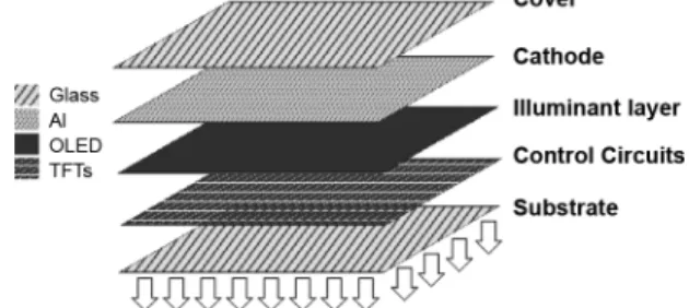
Unlike AM-LCD panels, which need a backlight element to be its light source, AM-OLED panels use the OLED thin film embedded in its multilayer structure for illumination and hence requires no backlight element. Fig. 1 illustrates the typical multi-layer structure used for an AM-OLED panel, which consists of the following five layers listed from bottom to top: 1) substrate layer; 2) control-circuit layer; 3) illuminant layer; 4) cathode layer; and 5) cover layer. The substrate layer and cover layer are usually made by glass, which allows the light passing through, isolates the other inner layers from water and oxygen, and hence prevents the aging of its organic material as well as the change of TFT’s electrical characteristics. The control-circuits layer utilizes TFTs and capacitors to form a pixel array, which can control the degree of illumination of each OLED, which is evaporated on the illu-minant layer accordingly. The cathode layer is made by metal Al and used as the ground signal connected to OLED.
As a result of the multilayer structure shown in Fig. 1, the panel’s images are observed from the bottom of the panel since the layer on top of the illuminant layer (made by aluminum) is opaque. Thus, the light generated by the OLEDs needs to pass through the control-circuit layer, and which in turn needs to pro-vide a transparent region on each pixel design as a channel for
Fig. 1. Typical multilayer structure of an AM-OLED panel.
Fig. 2. Layout of a typical pixel design and its resulting transparent region.
light. The transparent region is made by a transparent electrical conductor, indium tin oxide (ITO), and is used as an electropad connecting to the OLED. Fig. 2 shows a typical pixel layout with the corresponding transparent region. Based on the OLED technologies used in our design, the ratio of the transparent re-gion in a pixel design (defined as aperture ratio) have to be more than 40% of the pixel’s total area to provide sufficient luminance under the constraint of current density.
Following is the calculation of the minimum aperture ratio. First, we use (1) to calculate the required current passing through the OLED (denoted as ) such that the desired luminance of a panel (denoted as ) can be provided. In (1), the luminance of the panel is set to 200 nits 1 nit 1 Cd/m , which accords to the specification of a quality AM-OLED panel [9]. The pixel area (denoted as ) in a 4.1” QVGA AM-OLED panel is 86.78 260.35 m . The luminance efficiency (denoted as ) of the OLED in use is set to 4 Cd/A, which is a relatively weak OLED in current OLED market. The panel transmittance (denoted as ) is set to 0.8, which is determined by the transmittance of the transparent electropad (ITO) and the substrate (glass). By solving (1) with the above parameters, the required current is equal to 1.4 A
Fig. 3. Overview of a pixel array.
The aperture ratio of a pixel design (denoted as ) deter-mines the area of the transparent electropad, i.e., the area of the evaporated OLED. The area of the evaporated OLED further determines the current density of the OLED [10], [11]. An ex-cessive current density may significantly degrade the reliability and lifetime of the OLED. In the following calculation, we set the upper bound of the current density (denoted as ) to 20 mA cm as suggested by [10], [11]. By solving (2), the aper-ture ratio needs to be larger than 31%. Thus, setting the min-imum aperture ratio to 40% is actually a high standard for cur-rent panels and can already cover a significant range of design margins
(2) Fig. 3 shows an overview of an AM-OLED pixel array locating on the control-circuit layer, where the lightness of a pixel is controlled by the data stored in a pixel cell. In this pixel array, a row of pixel cells is selected by the signal . The data of pixel cells on a selected row is fed through the signal
. The signal and are controlled
by an outside driving IC through a runner, respectively. Such an AM-OLED pixel array is similar to a DRAM array except the following differences: 1) the data stored in each AM-OLED pixel cell is an analog signal rather than a digital signal; 2) an AM-OLED array only performs write operations while a DRAM array performs both read and write operations; and 3) the write operation of an AM-OLED pixel array is performed in a row basis serially and ceaselessly while DRAM cells can be accessed randomly.
Fig. 4 illustrates the typical pixel design used in current AM-OLED displays, which consists of two TFTs, one capac-itor, and one OLED. As shown in Fig. 4, the lightness of an OLED is determined by the current flowing through the TFT , which is further controlled by the display data stored in the capacitor . The TFT functions as a switch for deter-mining whether the data from should be written in the capacitor according to signal of . With this pixel design, the electric signal stored in the capacitor can be transformed into an optical signal displaying on an OLED.
Fig. 4. Schematic of the typical pixel design.
Fig. 5. Exemplary timing diagram of Scan line and Data line for an AM-OLED pixel array.
Fig. 5 shows an exemplary timing diagram of
and on an AM-OLED pixel array. The signals on are sequential and non-overlapped pulses. The signal on represents the image data to be displayed on a pixel row and is notated by , where and represent the index of the corresponding pixel row and time frame, respectively. When on a row is turned on, the cor-responding pixel cells enter the “data-written” phase and their display data is written in. When on the row is turned off, the corresponding pixel cells enter the “data-retained” phase and the pixel cells need to maintain the stored data until the next write operation on the current row. Thus, the time of an image frame is equal to the total time of a data-written phase and a data-retained phase, which is actually equal to the total number of rows times the time of a data-written phase.
Therefore, the quality of a proposed pixel design can be de-termined by its required time of writing in a display data and its capability of retaining a display data. The time of an image frame is fixed and usually set to 16.7 ms (reciprocal of 60 Hz) according to the sensitivity of human’s vision. Thus, the time of a data-written phase determines the number of pixel rows to be supported in a display, i.e., the size of the display. The capability of retaining a display data affects the degree of display-data vari-ation during the data-retained phase, and in turn determines the contrast resolution represented by its least significant bit. Also, the proposed pixel design has to be subject to the pixel-area limit of a display panel and the required aperture ratio.
Fig. 6. I versus V of a nc-Si TFT [1].
III. CHALLENGE OF USING NC-SI TFTS IN AM-OLED DISPLAYS
A. Problem: High Leakage Current of nc-Si TFTs
Despite of providing several advantages on its mobility, reli-ability, and manufacturing cost, the nc-Si TFTs suffers from its large turn-off leakage current [1], [3], [5], [12], which does not exist for -Si TFTs or can be solved by using lightly-doped-drain (LDD) technique for low-temperature-polysilicon TFTs, which is a poly-Si TFT technology [2]. Fig. 6 shows the drain-source current of a nc-Si TFT versus gate-source voltage in condition of different drain-source voltage [1]. As Fig. 6 shows, of a nc-Si TFT may significantly increase when is smaller than a certain amount. This characteristic of large turn-off leakage current results in that the switch TFT may not be able to cut off the connection between and (as shown in Fig. 4) during the data-retained phase. Thus, the data stored on would be interfered by the data at writing into the other pixel cells in the same column, which may result in significant display-data variation during the data-retained phase.
B. Straightforward Solutions
For the engineers who cannot acquire better TFT devices at present, the following two straightforward solutions can be ap-plied to the typical pixel design to minimize the display-data variation resulting from nc-Si TFT’s large leakage current. The first solution is to increase the refresh rate. The second one is to increase the size of the capacitor or the channel length of the TFT .
1) Higher Refresh Rate: The objective of increasing refresh
rate is to reduce the time of the data-retained phase such that the variation of the stored voltage of can also be reduced before the new display data is written in. However, increasing the refresh rate may result in the following three drawbacks. First, increasing the refresh rate needs a stricter specification to both the data-driver IC and the scan-driver IC, which may in turn increase the design efforts and the cost of both driver ICs. Second, increasing the refresh rate requires a higher power consumption of the display, which may prevent the AM-OLED displays from mobile applications. Last and most importantly, the time for writing in display data to a pixel cell needs to be
reduced since a frame period is equal to the total number of pixel rows times the time of the data-written phase. Otherwise, the number of affordable pixel rows become smaller. The time of writing in a display data is determined by the mobility and the channel width of the switch TFT . However, increasing the mobility of a TFT may not be always achievable and increasing the channel width of the switch TFT may increase its leakage at the same time, which contradicts with our original objective of using a higher refresh rate.
2) Larger or Longer Channel Length of : This
cir-cuit-level solution focuses on increasing the time constant between and , where and represent the capacitance of and the drain-source resistance of during the data-re-tained phase (which is also denoted as ). Usually, in-creasing is not preferable because the layout area of already occupies a significant portion of the whole pixel design. Doubling the size of may significantly decrease the aper-ture ratio of the pixel design. Also, increasing the size of will increase the time of writing in a display data. On the other hand, increasing the channel length of is more affordable since the original size of is relatively small. For current typ-ical pixel designs, the channel length of can be increased by multiple times and its aperture ratio can still be higher than the minimum requirement. Also, increasing the channel length of will increase the time of writing in a display data as well. Thus, when increasing the channel length of , both aperture ratio and the capability of writing in a display data should be maintained higher than their minimum requirement.
IV. PROPOSED PIXEL DESIGN FORMINIMIZING DISPLAY-DATAVARIATION
A. Design Overview and Design Constraints
In this section, we propose a novel pixel design to minimize the display-data variation resulting from the large leakage cur-rent of nc-Si TFTs. Fig. 7 shows the schematic of the proposed pixel design, which consists of three TFTs ( , , and ), three capacitors ( , , and ), and one OLED. Compared to the typical design shown in Fig. 4, TFT in the proposed pixel design plays the same role as TFT in the typical de-sign, which connects a voltage source to the OLED. Instead of using only one capacitor in the typical pixel design, the proposed pixel design uses three capacitors ( , , and ) to store the display data. Also, the proposed pixel design utilizes two TFTs ( and ) as switches to determines whether the display data can be written in. The voltage at determines the lightness of the OLED.
The proposed pixel design can effectively minimize the dis-play-data variation by adding an extra TFT in between the stored display data (voltage at ) and during the data-written phase. Also, the proposed pixel design requires no extra
control signal other than and , and thus
can be easily applied to current AM-OLED displays using nc-Si TFTs. However, in order to limit the area overhead and provide an enough aperture ratio, two design constraints need to be fol-lowed for the proposed design. First, the total capacitance of , , and is the same as . Second, the size of each TFT used in the proposed design is the same as that used in
Fig. 7. Schematic of the proposed pixel design.
the typical design. With these two constraints, the area over-head of the proposed pixel design is around one TFT more com-pared to the typical design, which is within the affordable range based on the aperture ratio of our current pixel design. Actually, this 1-TFT area overhead can be further minimized using proper layout techniques. Note that we strictly limit the size of the total capacitance because the capacitor in the typical pixel design al-ready occupies a big portion of the pixel-cell layout. Any further significant increase of the capacitance may result in large area overhead and in turn an unacceptably low aperture ratio.
In the following Sections IV-B and IV-C, we will first detail the behavior of the proposed pixel design during the data-written phase and the data-retained phase, respectively. Next, we will compare the proposed pixel design with the typical pixel design based on the result of analysis, simulation, and measurement. Also, we will discuss the impact of using different combinations of the sizes of , , and on the display-data variation and the data-written time.
B. Circuit Behavior During Data-Written Phase
During the data-written phase, is set to high and both and are turned on. Once is turned on, the volt-ages at the two terminals of , , and , are about the same. Then similar data voltage will be written into through one TFT and be written into through two TFTs ( and ). As a result, the discharge of is relatively small during the data-written phase. Since writing data into needs to pass a larger resistance (one more TFT) than writing data into , a smaller ratio of over can reduce the write time of the proposed pixel design.
C. Circuit Behavior During Data-Retained Phase
At the beginning of the data-retained phase (right after the data-written phase ends), the voltages at and should be the same and represent the display data (the impact of the par-asitic capacitance of and is ignored here). At the same time, is set to low and both and are turned off. Due to the leakage of and , the data at and may be changed. The amount of the leakage current is strongly de-termined by the TFT’s drain-source voltage. As shown in Fig. 6, the leakage current when 10 volt could be 3-order larger than the leakage current when 0.1 volt. Thus, the leakage
of can be much larger than that of since the voltage be-tween and is significant larger than the voltage between and (almost 0 at the beginning of the data-re-tained phase).
Compared to the typical pixel design shown in Fig. 4, the data variation at is larger than that at since the capacitance of
is smaller than that of . However, the data variation at is significantly smaller than that at due to a smaller leakage current of . Note that the voltage at represents the display data during the data-retained phase. Thus, the key idea of the proposed design is to protect the data at by creating a smaller drain-source voltage of while allowing a larger but proper data variation at . In our later analysis, we will discuss how the setup of the size of , , and affects the data variation at for the proposed pixel design.
In fact, the voltage between and will increase with time, and in turn may degrade the capability of the proposed pixel for protecting its display data after a certain period of time. Fortu-nately, this situation only occurs after the time passes the period of the data-retained phase. Thus, the proposed pixel design can still effectively protect its display data for current applications of display panels.
V. WORST-CASEANALYSIS FOR THEPROPOSEDPIXELDESIGN In this section, we theoretically analyze the degree of dis-play-data variation and the time of writing in a display data for the proposed pixel design, respectively. Also, the analysis for both data variation and write time is performed under their worst case.
A. Worst-Case Display-Data Variation
The leakage current of a transistor is directly proportional to its drain-source voltage. Thus, the worst case of display-data variation of a pixel occurs when the display display-data of the pixel stores the maximum voltage (denoted as ) and its stays constantly at the minimum voltage (0 volt) during the data-retained phase. Based on this worst-case setting, we then analyze the display-data variation for both the typical and proposed pixel designs, i.e., to calculate the voltage at in Fig. 4 and the voltage at in Fig. 7 with respective to time
, respectively.
1) Display-Data Variation of the Typical Pixel Design: The
current flowing in the transistor is equal to the current flowing out of the capacitor during its discharging. Thus, the voltage at node (denoted as ) can be determined by (3), where represents the resistance of when turns off
(3) By solving the differential equation of (3), we can obtain versus time as shown in (4). Note that the boundary condition is
when
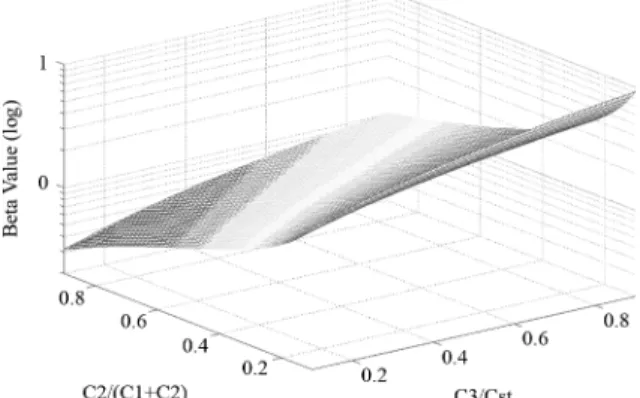
Fig. 8. Beta value associated with different settings ofC , C , and C when t = 0:01 3 R 3 C .
Fig. 9. Beta value associated with different settings ofC , C , and C when t = 0:1 3 R 3 C .
Based on (4), we can then derive the derivative of with respect to time as listed in (5)
(5)
2) Display-Data Variation of the Proposed Pixel Design: To
analyze the voltage at (denoted as ) for the proposed pixel design, we need to analyze the voltage at (denoted by ) first. During the data-retained phase, the turn-off resistance of
(denoted as ) can be viewed as infinite since its is low and the leakage current is much smaller than that of . As a result, the equivalent capacitance at is
during the data-retained phase, where represents the equivalent capacitance when is connected to in serial.
Thus, by substituting with and
with in (5), we can obtain the derivative of with respect to time as listed in (6)
(6) Because of the charge sharing between and , the rela-tion between and can be obtained as in (7)
(7)
By substituting with (6), we obtain the derivative of with respect to time as shown in (8)
(8)
3) Comparison Between the Proposed and Typical Pixel De-signs: To evaluate the effectiveness of the proposed pixel deign
on reducing the display-data variation, we first define the factor as the ratio of over . A larger value of means that the proposed pixel design can protect its display data better from the transistor’s leakage compared the typical pixel design. Equation (9) shows the calculation of by combining
(5) and (8). Note that since the
transistors used in both designs have the same device size
(9) Equation (9) shows that the value of is affected by the fol-lowing factors: 1) the turn-off resistance of the transistor; 2) the size of each capacitor ( , , , and ); and 3) the time . Figs. 8 and 9 show the logarithm of associated with
and when and
, respectively. From Figs. 8 and 9, we find the following two trends about the value of . Note that
.
• A larger out of the total capacitance leads to a higher .
• A smaller out of leads to a higher .
The reason for the first trend is that a larger can mini-mize the voltage variation at , which in turn can minimize the voltage variation at as shown in (7). The reason for the second trend is that a smaller can minimize the voltage variation at caused by the charge sharing between the serially connected and .
Fig. 10 shows the value of over time for three different settings of , , and . Note that the turn-off resistance of a TFT varies along with its as shown Fig. 6, where ranges from 10 volt A to 0.1 volt A, i.e., 10 to 10 . With 200 fF, the time represented by
here should be between 20 and 200 ms (average 110 ms). Since the period of the data-retained phase defined in the specification is 16.7 ms (corresponding to 60 Hz), we care only the value of before . During this period (0 to ) in Fig. 10, the value of is almost a constant for all capacitance settings.
However, the above analysis is only an approximation since the TFT transistor is assumed to be fully turned off during the data-retained phase. In reality, a smaller may not always lead to a higher because a larger can help to reduce the vari-ation of of and in turn limit the leakage current of . Fig. 11 shows the of over time with different values of
Fig. 10. over time for three capacitance settings.
Fig. 11. V ofM over time associated with different values of C given C =C = 0:8.
, where the of increases while decreases. If a too small is used, the leakage of will significantly increase, which will then speed up the voltage variation at . Thus, the size of should be controlled within a proper range to mini-mize the display-data variation. This constraint also implies that the size of cannot be too large since the total capacitance of , , and is a constant . A too large will limit the size of .
Since the of is originally 0 at the beginning and then gradually becomes larger, the leakage of becomes larger along with the time, meaning that the proposed pixel design can only protect its display data effectively at the early stage and may gradually lose its capability of data protection later on. Fortunately, the increase of the of in our proposed pixel design is not significant enough during the data-retained phase defined in our specification (16.7 ms, reciprocal of 60 Hz). Thus, compared to the typical design, the proposed pixel design can still effectively protect the display data with a proper setting of its three capacitors. We will show the simulation result to validate this phenomenon in the next section.
B. Worst-Case Write Time
In this subsection, we analyze the worst-case write time, i.e., writing a into a pixel whose original value is 0 volt, for both typical and proposed pixel designs. The write time of a pixel design is determined by its equivalent time constant.
Fig. 12. Illustration of theRC model during the data-written phase for both the typical and proposed designs.
Fig. 12 illustrates the simplified model for both the typical and the proposed new pixel design, where represent the resistance of the transistor when turns on.
Based on the model of Fig. 12, (10) and (11) shows the worst-case write time for the typical design (denoted as ) and the proposed design (denoted as ), respec-tively. Note that the transistors on both designs have the same device size and hence
(10)
(11) In fact, the in (11) represents the upper bound of the worst-case write time of the proposed design. The term
is overestimated since the voltage between and is small during the data-written phase (small ) and is not fully discharged. If we completely ignore the impact of and eliminate the term from (11), a lower bound of the worst-case write time can be obtained as in (12)
(12) As (11) shows, the upper bound of the worst-case write time of the proposed design is more than that of the typical design. As (12) shows, the lower-bound of the worst-case write time is less than the upper bound. Thus, to reduce the write time for the proposed design, needs to be smaller and
needs to be larger. However, a smaller and a larger may decrease pixel’s capability of protecting the display data. In Section VI, we discuss how to find a proper setting of all capacitors used in the proposed pixel design through simulation.
VI. SIMULATIONRESULTS
In this section, we will discuss the following issues through the simulation results, which are performed based on the PECVD-based bottom-gate nc-Si-TFT technology developed by ITRI [8].
A. Worst-Case Display-Data Variation
In the following experiment, we simulate the display-data variation of the proposed design by using different settings of its capacitors ( , , and ), and then compare it to that of the typical design. The display-data variation is defined by the
Fig. 13. 1V =1V associated with different capacitance settings.
biggest voltage difference to its original stored voltage (at or ) caused during a whole data-retained phase. We use and to denote this display-data variation for the typical and the proposed designs, respectively. The stored display data here is set to , i.e., 10 volt in our specification, and its is enforced to stay at 0 volt such that the leakage current of the pixel can be the worst. The total capacitor in use is 200 fF. The channel length and width of a TFT tran-sistor are both 8 m. The period of a data-retained phase is 16.7 ms (reciprocal of 60 Hz). Fig. 13 shows the ratio of over
for different combination of and ,
where .
As the result shows, Fig. 13 confirms our inferences about display-data variation in Section V-A. First, in-creases when increases initially but then starts to drop after is larger than a certain value. Second, also in-creases when decreases initially but then starts to drop after is smaller than a certain value. The peak of
oc-curs when and . Also,
the peak value of is more than 5.65, meaning that the proposed design can effectively reduce the data variation by 5.65 times compared to the typical design.
Next, Fig. 14 shows the and versus time, given that
200 fF, , and .
The rest experiment setting is the same as that used for Fig. 13. As the result shows, the display data of the proposed design drops much slower than the typical design at the begin-ning but then drops faster after a certain period of time. In this experiment, starts to drop faster than when is larger than 37.5 ms, which is much longer than the normal specifi-cation of the data-retained phase, 16.7 ms. This result further demonstrates the effectiveness of the proposed pixel design on reducing the display-data variation for practical applications of display panels.
B. Worst-Case Write Time
Fig. 15 shows the ratio of the worst-case write time of the proposed design (denoted as ) over that of the typical design (denoted as ) for different capacitance settings. As the result shows, the write time of the proposed design decrease when increases or decreases, which fits the conclusion of our analysis in Section V-B.
Fig. 14. Stored display data over time for both the typical and proposed designs.
Fig. 15. W T =W T associated with different capacitance settings.
Fig. 16. W T =W T versusC =(C + C ) when C =C = 0:6.
Fig. 16 further shows the obtained by the sim-ulation, the upper bound in (11), and the lower bound in (12)
when is set to 0.6 and varies. The result
again confirms our analysis on the write time for the proposed design.
C. Finding a Proper Capacitance Setting
In general, the write time of the pixel design is usually a con-straint instead of a factor to be minimized. Thus, in this subsec-tion, we attempt to find a capacitance setting for the proposed design which can result in the largest under the constraint that its is not more than 1.15. We first find the capacitance setting with the largest ,
Fig. 17. 1V =1V and W T =W T versus C =C when C =(C + C ) = 0:32.
Fig. 18. 1V =1V and W T =W T versus C =(C + C ) when C =C = 0:86.
i.e., and as shown
in Fig. 13. For and ,
its is 5.65 but its is 1.17, which
exceeds the constraint of 1.15. We then search around the ca-pacitance setting around the peak point, and
. Fig. 17 shows both and
when is fixed at 0.32 and
varies. As the result shows, the improvement of the proposed de-sign on the display-data variation drops rapidly when is over 0.86 but the corresponding write time does not drop signif-icantly. Thus, appears to be the best setting.
Next, Fig. 18 shows and
when is set to 0.86 but varies. As the
result shows, the improvement on the display-data variation stays around the same level when is near the peak point 0.32. Thus, we can then choose the capacitance setting in Fig. 18 which results in the largest
with , i.e., and
. Its improvement on display-data variation can
be 5.55 and its is exactly 1.15.
Note that designers may need to consider more design param-eters other than the write time and the display-data variation, such as layout area or aperture ratio. The capacitance setting for the proposed design should be chosen based on the corre-sponding objective and design constraints in use. In fact, several capacitance settings in Fig. 13 can achieve a close to the maximum. The designers could utilize those settings for optimizing other design parameters.
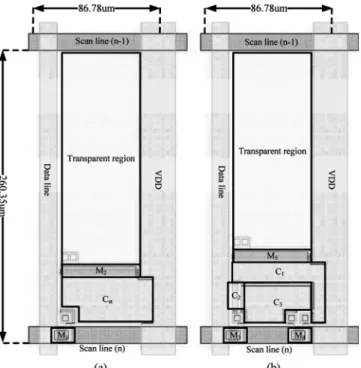
Fig. 19. Layout of the typical and proposed designs for a 4.1” QVGA color AM-OLED panel. (a) Typical design. (b) Proposed design.
D. Area Overhead and Aperture Ratio
Fig. 19(a) and (b) illustrate the layout of the typical pixel design and the the proposed pixel design, respectively. Both pixel designs follows the specification of 4.1” QVGA color AM-OLED backplanes. Its resolution is 320xRGBx240 and its pixel size is 86.78 m 260.35 m for each of the red, green, and blue pixels. For our application, we utilize a white-light OLED along with a corresponding color filter to generate each of RGB colors instead of using an individual OLED which can directly generate the corresponding color. Thus, the pixel sizes as well as their required aperture ratios are the same for all red, green, and blue pixels.
Compared to the typical design, the area overhead of the pro-posed pixel design is an extra transistor . The total ca-pacitances for both designs are the same. However, as shown in the bottom-right of Fig. 19(b), this transistor can be placed above the metal of , and hence its resulting area overhead for the control design can be reduced, which in turn limits the decrease of the aperture ratio for the proposed design. Overall, the aperture ratios of the the proposed design is 41.4%, which is 3.2% lower than that of the typical design (44.6%) and is still higher than the minimum requirement of the aperture ratio (40%) for most AM-OLED displays. This 3.2% lose on the aperture ratio results from the extra contact holes and the spacing around the two more capacitors enforced by the design rules.
Note that, for both typical and proposed designs, the area oc-cupied by the capacitors is much more than that ococ-cupied by the transistors. That is why we are only willing to spend extra area for transistors to reduce the display-data variation, but not extra area for capacitors. The same percent increase in the total capacitance can result in a significant lose in its aperture ratio.
Fig. 20. Improvement of the contrast resolution achieved by using the proposed pixel.
In addition, for the AM-OLED applications which require a higher requirement of the aperture ratio, we can further elimi-nate the metal line with other signal metal lines [13]. Also, top-emission scheme can be used to provide a higher aperture ratio [14], [15].
E. Improvement on Contrast Resolution
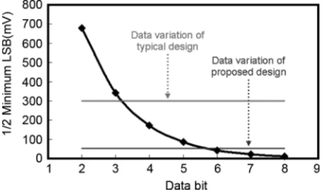
In this subsection, we attempt to identify the contrast reso-lution which can be achieved by our current nc-Si-TFT tech-nology [8] with and without applying the proposed pixel design. The supportable contrast resolution for a nc-Si-TFT technology is determined by its display-data variation during the data-re-tained phase and the voltage of its LSB (least-significant-bit) after -correction. As long as the corresponding display-data variation is less than one half of the LSB voltage, this contrast resolution is supportable.
Fig. 20 shows one half of the LSB voltage required by dif-ferent numbers of resolution bits. Also, Fig. 20 shows the dis-play-data variation caused by the typical design and the pro-posed design, respectively. As the result shows, the typical de-sign can only support a 3-bit contrast resolution with our current nc-Si-TFT technology while the proposed design can support a 5-bit contrast resolution. For general display applications, the number of resolution bits is 8.
VII. OTHERISSUES FOR THEPROPOSEDPIXELDESIGN
A. Turn-Off Voltage at Scan Line
As Fig. 6 shows, does not always decrease when decreases, meaning that decreasing the turn-off voltage at
may not be always able to decrease the leakage current. Also, the leading to the minimum also varies with different . Thus, in this subsection, we attempt to find an appropriate turn-off voltage at (denoted as ) such that the display-data variation for a pixel can be minimized. We first denote the leading to the minimum
given as . In Fig. 6,
is 6.41 volt and is 8.48 volt, where
10 volt and 0 volt.
The ideal case for a good setting of is that its resulting
can be close to for each . However,
is determined by the voltage at , which may vary randomly and hard to predict. Also, is determined by the
Fig. 21. Worst-case display-data variation versusV .
voltage of the stored data, which further determines the corre-sponding . It makes the analysis for the best even harder. Thus, we can only know that the best should
be around since the scale of when
is several orders larger than that when . Fig. 21 shows the display-data variation with different set-tings of , where the store data is set as to create a worst case and the voltage at is a full-range triangle wave to approximate the random data in real applications. As the re-sult shows, the display-data variation can be minimized when setting the turn-off voltage at to 5.5 volt, which is
(-6.41 volt) plus a small constant.
B. Coupling Effect
The coupling effect of a pixel design is referred to the transient voltage drop of the stored data caused by the signal transition at (from 1 to 0) interacting with the parasitic capaci-tors of switch transiscapaci-tors. As a result, at the beginning of the data-retained phase, the stored value first drops by the coupling effect and then varies by switch transistor’s leakage (discussed as data variation previously). This coupling effect has been ex-isted on the pixel designs of AM-LCD and AM-OLED displays. Fig. 22(a) illustrates the coupling effect on the typical pixel de-sign of AM-OLED displays. Fortunately, on the typical pixel design, the voltage drop caused by the coupling effect is almost a constant value for different stored data voltages. It means that by elevating every stored data voltage with a fixed constant, the displayed lightness can remain almost the same as if no cou-pling effect exists. This solution to the coucou-pling effect can be implemented easily without significant overhead [16] and has already been used for AM-LCD displays.
For the proposed pixel design, the coupling effect becomes larger since the impact of two more parasitic capacitors ( and ) of is taken into account other than the of
[as shown in Fig. 22(b)]. Fig. 23 shows the voltage drop caused by the coupling effect corresponding to each stored data voltage on the typical design (denoted by ) and the proposed designs with 3 arbitrary capacitance settings (denoted by ,
, and ). The capacitance settings are ,
; ,
; and , . As the
result shows, the voltage drop of the proposed design is around the same for each stored data voltage just like the typical design, and the same trend can be observed on different capacitance
Fig. 22. Parasitic capacitance of the switch TFTs for both the typical and the proposed pixel design. (a) Typical design. (b) Proposed design.
Fig. 23. Coupling effect associated with different stored data for the typical and proposed designs.
settings of the proposed design. It means that the coupling effect can also be solved for the proposed design with the same simple solution described above.
VIII. MEASUREMENT OFFABRICATEDTFT CIRCUITS
A. Measurement Procedure
We have fabricated both the typical and the proposed pixel design using the PECVD-based bottom-gate nc-Si-TFT tech-nology developed by ITRI [8]. Fig. 24 shows the photo of a fabricated die, which contains several single pixel designs with different configurations. If we directly probe the voltage of the stored data ( or ), the prober of the oscilloscope will im-pose a 10 pF capacitance and a 1 M resistance to the pixel de-sign. Thus, we need to measure the voltage at the source of the transistor driving the OLED through an IO pad and then infer the voltage of the corresponding stored data. Fig. 25 illustrates the measurement setting for both the typical and the proposed designs. Note that the fabricated pixel designs are not connected
Fig. 24. Photo of the fabricated die.
Fig. 25. Measurement setting for both the typical and proposed designs. (a) Typical design. (b) Proposed design.
to any OLED. The OLED is replaced by an IO pad for measure-ment use.
In order to infer the stored data of a pixel ( or ), we need to build the relation between the voltage at the gate (de-noted as ) and the voltage at the source (denoted as ) of the TFT transistor driving the OLED (i.e., or ). For the fab-ricated typical and proposed designs, the device dimension of both and is 40 m 8 m. Fig. 26(a) illustrates how we built the relation between and of (or ), where we generate a 1 Hz triangle wave ranging from 0 volt to 10 volt at and then measure the corresponding through an IO pad. The transistor’s drain is connected to (10 volt). Fig. 26(b) shows the measured versus . Due to the noise of the mea-sured result, we utilize a monotonically-increasing sixth-order polynomial to fit this curve and use the polynomial to map the measured to . Note that this relation between and is characterized combining the effect of the prober’s parasitic
Fig. 26. V versus V of the TFT driving the OLED.
Fig. 27. Signal atScan line and Data line and an exemplary measured result.
capacitance and resistance, which is exactly the same condition when measuring the fabricated pixel designs. Thus, no compen-sation needs to be added into this characterized relation when it is used to infer the stored data of a pixel design.
Fig. 27 shows the signal at and during
our measurement as well as an exemplary measured voltage at the output IO pad (denoted as ). When just turns on, keeps on 0 volt for 5 ms to make sure that the stored data is set to 0 volt. Next, is set to 10 volt and we start to measure the write time. After another 5 ms, we turns off and start to measure the display-data variation during the next 16.7 ms (the period of the data-retained phase). Note that, due to the coupling effect mentioned previously, the voltage setting of the has been slightly adjusted for equal stored data in both the typical and the proposed design.
To obtain the display-data variation, we measure the highest (denoted as ) and the lowest (denoted as ) during the 16.7 ms data-retained phase. Then we map and into their corresponding (or ) using the characterized relation shown in Fig. 26(b). The difference between the two mapped is the measured display-data variation.
To obtain the write time, we measure the time from
to (denoted as ), where is the maximum
voltage when is on. The measured write time is equal to minus the gate-source delay of the transistor. Fig. 28 shows how we obtain the gate-source delay, where a square wave is generated at the gate and measure the time when reach the top. In fact, we only choose to use the time when
Fig. 28. Measurement of the gate-source delay.
TABLE II
MEASUREMENTRESULTS FOR3 DIFFERENTCONFIGURATIONS OF THE
TYPICALPIXELDESIGN
reaches the 98% of the top as the gate-source delay since the signal above the 98% vibrates severely and it takes long time to reach the true top of . Similarly, when measuring , we also choose the time when the measured reaches the 98%
of .
B. Measurement Result
Table II lists the measured display-data variation and write time for three configurations of the fabricated typical pixel de-signs, denoted as T-1, T-2, and T-3. The difference among the three configurations is the channel length of their TFT tran-sistor, where the channel length of T-2 and T-3 is double and triple of that of T-1, respectively. The reported display-data vari-ation for a configurvari-ation T-x is actually a ratio compared to that of T-1, which is of T-1 over of T-x. The reported write time for a configuration T-x is the write time of T-x over that of T-1.
As the result shows, increasing the channel length of can indeed reduce the display-data variation. However, its write-time overhead is directly proportional to its channel length. If we triple the channel length, its measured write time will in-crease more than 3 times. Also, its improvement on display-data variation is only 2.38. This result further demonstrates that in-creasing the channel length of is not a cost-effective method to reduce the display-data variation.
Table III lists the measured display-data variation and write time for nine configurations of the fabricated proposed pixel de-signs, denoted as P-1 to P-9. Each configuration utilizes a dif-ferent capacitance setting with 200 fF. The device dimen-sion of both and for all nine configuration is 8 m 8 m. Similar to Table II, the reported display-data variation and write time is a ratio compared to that of the typical design using T-1 configuration.
As the result shows, the reported display-data variation and write time fit our analysis and simulation results. Basically, a larger can result in a lower display-data variation and a shorter write time before reaching its optimal point (
TABLE III
MEASUREMENTRESULTS FORNINEDIFFERENTCONFIGURATIONS OF THE
PROPOSEDPIXELDESIGN
result in a shorter write time. Compared to that of the typical de-sign T-1, the best improvement on display-data variation among the nine fabricated proposed designs is 4.06 with only 1.36 write time. This result again validates the effectiveness of the proposed pixel design based on real fabricated TFT circuits.
IX. CONCLUSION
In this paper, we have introduced a novel pixel design to re-duce the data variation caused by the leakage current of nc-Si TFT. We first theoretically analyzed the trend of its worst-case data variation and its worst-case write time. Next, several simu-lations associated with different capacitance settings were con-ducted to verify the correctness of our analysis. As the result shows, the proposed pixel design can achieve a 5.55 reduc-tion on its data variareduc-tion while requiring only 1.15 write time when compared to the typical pixel design. The resulting con-trast resolution can also be improved by two bits. In addition, the area overhead of the proposed pixel design can be effec-tively limited by the layout techniques, and thus the proposed design can still provide an aperture ratio over 40%. We further discussed the proper setting of the turn-off voltage at
and the impact of the coupling effect on the proposed pixel de-sign. At last, we reported the measurement results based on the PECVD-based bottom-gate nc-Si-TFT technology devel-oped by ITRI [8].
ACKNOWLEDGMENT
The authors would like to thank DTC, ITRI for discussion and assistance with fabrication.
REFERENCES
[1] K. S. Girotra, Y. M. Choi, B. J. Kim, Y. R. Song, B. Choi, S. H. Yang, S. Kim, and S. Lim, “PECVD-based nanocrystalline-silicon TFT back-planes for large-sized AMOLED,” J. SID, vol. 15/2, pp. 113–118, 2007. [2] T. Arai, N. Morosawa, Y. Hiromasu, K. Hidaka, T. Nakayama, A. Makita, M. Toyota, N. Hayashi, Y. Yoshimura, A. Sato, K. Namekawa, Y. Inagaki, N. Umezu, and K. Tatsuki, “Micro silicon technology for active matrix OLED display,” SID, vol. 41.2, pp. 1370–1373, 2007. [3] M. R. Esmaeili-Rad, A. Sazonov, and A. Nathan, “Analysis of the off
curent in nanocrystalline silicon bottom-gate thin-film transistors,” J.
Appl. Phys., vol. 103, p. 074502, 2008.
[4] Y. H. Peng, C. H. Chen, C. C. Chang, Y. S. Lee, T. S. Huang, C. Y. Hou, K. F. Huang, and Y. Y. Tseng, “32-inch LCD TV using conventional PECVD microcrystalline-silicon TFTs,” SID, vol. 24.3, pp. 333–336, 2008.
[5] C. H. Lee, D. Striakhilev, S. Tao, and A. Nathan, “Top-gate TFTs using 13.56 MHz PECVD microcrystalline silicon,” IEEE Electron Device
Lett., vol. 26, no. 9, pp. 637–639, Sep. 2005.
[6] K. Girotra, S. Park, J. M. Huh, C. Hong, K. Park, S. Lee, J. H. Lee, C. Chu, J. Goh, J. Choi, C. Kim, and J. H. Souk, “A 14inch uniform AMOLED display with low cost PECVD based microcrystalline sil-icon TFT backplanes,” SID, vol. P-259L, pp. 1289–1292, 2008. [7] C. Y. Chang, Y. S. Lee, T. Y. Huang, P. S. Shih, and C. W. Lin,
“The effect of microcrystalline silicon film structure on low-high-low band-gap thin film transistor,” Mater. Chem. Phys., vol. 62, pp. 153–157, 2000.
[8] Y. Y. Pan, C. M. Yeh, C. N. Li, H. Y. Fang, and Y. C. Chen, “Micro-crystalline silicon thin film deposition technology,” Ind. Mater., vol. 271, p. 112, 2009.
[9] AU Optronics Corp. (AUO), “AU Optronics successfully develops world’s first double sided active matrix OLED,” 2004.
[10] W. J. Nam, C. Y. Kim, J. H. Lee, S. G. Park, and M. K. Han, “High-aperture ratio pixel design employingV line elimination for re-ducing OLED current density,” SID, vol. 36, pp. 1456–1459, 2005. [11] C. Adachi, “OLED characteristics at high current density,” Lasers
Electro-Optics Soc., vol. 2, pp. 594–595, 2003.
[12] A. T. Hatzopoulos, N. Arpatzanis, D. H. Tassis, C. A. Dimitriadis, M. Oudwan, F. Templier, and G. Kamarinos, “Study of the drain leakage current in bottom-gated nanocrystalline silicon thin-film transistors by conduction and low-frequency noise measurements,” IEEE Trans.
Electron Devices, vol. 54, no. 5, pp. 1076–1082, May 2007.
[13] W. J. Nam, C. Y. Kim, J. H. Lee, S. G. Park, and M. K. Han, “High-aperture ratio AMOLED pixel design employingV line elimination for reducing OLED current density,” SID, vol. 44.3, pp. 1456–1459, 2005.
[14] W. K. Chen, C. W. Ko, and S. H. Lee, “Bottom and top emission OLED pixel structure,” U.S. Patent 7 250 728, Jul. 31, 2007.
[15] C. J. Lin, “Top emission active matrix OLED and fabrication method thereof,” U.S. Patent 6 943 372, Sep. 13, 2005.
[16] Y. H. Tai, “Design and operation of TFT-LCD panels,” Wu-Nan
Cul-ture Enterprise, vol. 3, pp. 97–100, 2006.
[17] D. Dosev, T. Ytterdal, J. Pallares, L. F. Marsal, and B. níguez, “DC SPICE model for nanocrystalline and microcrystalline silicon TFTs,”
IEEE Trans. Electron Devices, vol. 49, no. 11, pp. 1979–1984, Nov.
2002.
[18] M. S. Shur, M. D. Jacunski, H. C. Slade, A. A. Owusu, T. Ytterdal, and M. Hack, “Spice models for amorphous silicon and polysilicon thin film transistors,” Electrochem. Soc. Proc., vol. 242, pp. 96–23, 1996. [19] P. Servati and A. Nathan, “Modeling of the reverse characteristics
of a-Si:H TFTs,” IEEE Trans. Electron Devices, vol. 49, no. 5, pp. 812–819, May 2002.
[20] C. W. Han, M. K. Han, M. S. Kim, W. J. Nam, S. J. Bae, K. Y. Kim, and I. J. Chung, “Top-emitting OLED pixel employing cathode-contact structure with a-Si:H thin-film transistors,” IEEE Electron. Lett., vol. 43, no. 11, pp. 623–624, Nov. 2007.
[21] M. H. Lu, E. Ma, J. C. Sturm, and S. Wagner, “Amorphous silicon TFT active-matrix OLED pixel,” in Proc. IEEE Lasers Electro-Optics Soc.
Annu. Meet., 1998, vol. 1, pp. 130–131.
[22] S. H. K. Park, M. Ryu, C. S. Hwang, S. Yang, C. Byun, J. I. Lee, J. Shin, S. M. Yoon, H. Y. Chu, K. I. Cho, K. Lee, M. S. Oh, and S. Im, “Transparent ZnO thin film transistor for the application of high aperture ratio bottom emission AM-OLED display,” SID, vol. 39, pp. 629–632, 2008.
[23] W. J. Nam, J. H. Lee, C. Y. Kim, H. J. Lee, and M. K. Han, “High-aperture pixel design employingV line elimination for active matrix organic light emitting diode display,” Japan. J. Appl. Phys., vol. 45, pp. 2433–2436, 2006.
Chen-Wei Lin received the B.S. degree from the Department of Electronics Engineering, National Chiao Tung University, Hsinchu, Taiwan, in 2006, and the M.S. degree from the Graduate Institute of Electronics Engineering, National Taiwan Univer-sity, Taipei, Taiwan, in 2007.
His current research interests include thin film transistor (TFT) circuitry design and VLSI design and testing.
Mango C.-T. Chao (M’07) received the B.S. and M.S. degrees from the Department of Computer and Information Science, National Chiao Tung University, Hsinchu, Taiwan, in 1998 and 2000, respectively, and the Ph.D. degree from the De-partment of Electrical and Computer Engineering, University of California, Santa Barbara, in 2006.
He is currently an Assistant Professor with the Department of Electronics Engineering, National Chiao Tung University. His current research interests include VLSI testing, TFT circuitry design, and physical design automation.
Yen-Shih Huang received the Ph.D. degree from the Department of Materials Science and Engineering, National Tsing Hua University, Hsinchu, Taiwan, in 2002.
He currently works with the Industrial Technology Research Institute, Taiwan. His current research in-terests include thin film transistor (TFT) devices and AMOLED panel manufacture techniques.
![Fig. 6. I versus V of a nc-Si TFT [1].](https://thumb-ap.123doks.com/thumbv2/9libinfo/7698322.144479/4.891.95.400.97.316/fig-i-versus-v-of-nc-si-tft.webp)