Thin Solid Films 346 (1999) 207-211
Room temperature oxidation of Cu/Sio.76Geo,2d
annealed at 200 to 300°C
Jian-Sting Luo”, Wen-Tai Lin”>*:, C.Y. Changb, P.S. Shihb
“Departrrwt of Muterinls Science and Engineering, National Cheilg Kung Uniwrsity, Tainatz, 7OIOI Taiwan hDeparttnent of Electronic Engineering, National Chiao Tung C’niwrsi& Hsinchu, Taiican
Received 14 October 1998: received in revised form 5 December 1998; accepted 5 December 1998
Abstract
The CuSi-catalyzed oxidation behavior of Cu/Si,1,7h Ge” :j after annealing at a temperature of 200-300°C was studied using transmission electron microscopy (TEM). For the Cu/Si o,-ioGeo,Z4 samples annealed at 300°C and followed by exposure in air for 14 weeks an SiOs layer embedded with precipitates containing Cu, Ge, Si, and 0 was formed on the surface of the Cu&Si!-Fe,,) film. During exposure the Cu atoms released from Cu@i,-,Ge,) by oxidation diffused down to the residual Si n.,hGeo?j f&n and subsequently the Si substrate to form new Cu&%,-,lGe,) and Cu$i, respectively. After exposure for 5-6 weeks not only the oxidation of the surface layer became severe but also the growth of the buried Si02 layer was initiated at the Cu3(Si,-,Ge,)/Cu$i interface. Concurrently, the Cu$i-catalyzed oxidation of Si by inward movement of the SiO#i interface was also observed. As compared with the annealed Cu/Si samples the presence of Ge significantly lowered the oxidation rate of the annealed Cu/Si,,7hGe ,I 24 samples. Higher temperature annealing promoted the oxidation rate because of Ge segregation out of the Cu&Si,-,,Ge,,) layer and the formation of a larger fraction of the Cu,iSi,-,Ge,,)/Cu$i interface where the buried Si02 layer was initially formed. 0 1999 Elsevier Science S.A. AU rights reserved.
Ke??vords: Cu$Sil-,Ge,); Room temperature oxidation; Ge segregation; Transmission electron microscopy
1. Introduction
As the device dimensions continue to shrink Cu is a potential material to replace Al for future metallization schemes because of its superior electrical conductivity and electromigration resistance [I]. Unfortunately, Cu is quite mobile in Si and its presence creates recombination centers which can reduce the minority-carrier lifetime [2]. The possible solution to this problem is the use of Cu;Si or Cu3Ge [3,4]. However, upon air exposure Cu$i reacts rzad- ily with oxygen at room temperature, while Cu3Ge is stable [P61. Many studies on the Cu$i-catalyzed oxidation of Si have been made [7-131.
Si,-,\Ge, material offers the promise of greater carrier mobility and band gap engineering, and hence has potential applications in high-speed electronic and optoelectronic devices [14]. The formation of metal-Si,-,Ge,, ohmic or rectifying contacts is required for device applications. Recently, the interfacial reactions of metals such as Ni [l.S], Pt [16], Pd [17], Ti [18-201, Co [21,22], and 0.1 [23] on Si,-,YGe,Y films have been studied. In these reactions, the growth of a ternary phase, e.g. M(Si,-,,Ge.,)z, was generally
* Corresponding author. Tel.: + 8-86-2757-575; fax: t g-86-234-6290.
E-mail address: [email protected] (W.T. Lin)
accompanied by Ge segregation and the formation of agglomeration structure.
For the CuBi,-,Ge, system Jaquez et al. [23] have shown that Ge plays an important role in slowing the rate of oxygen incorporation into the Cu germanosilicide. To date, as far as we know, the oxidation behavior for the Cu/Sil-,YGe, system after annealing has not been detailed. In this paper, we report the evolution of room temperature oxidation in air for the Cu/Si~.-ihGeo2~ system after annealing at a tempera- ture of 200-300°C using transmission electron microscopy (TEM) in conjunction with energy dispersive spectrometry (EDS). A simultaneous study of the Cu+Si/Si system was also conducted for comparison.
2. Experimental
%!.76G%24 films, about 150 nm thick, were grown at
550°C in an ultrahigh vacuum chemical vapor deposition system. A Cu layer, about 70 nm thick, was deposited onto the Si0,76Ge0,21 films at a rate of 0.1 rim/s in an electron gun deposition system. The base pressure was about 2.0 x
lop6 Torr. An amorphous Si overlayer, 10 nm thick, was subsequently deposited onto the Cu layer to protect the unreacted samples from oxidation during storage in a cham- OO40-6090/99/$ - see front matter 0 1999 Elsevier Science S.A. All rights resewed.
308 J.S. Lim er of. / i’%in Solid Films 346 (1999) 207-211
22
88
133
Depth (nm)
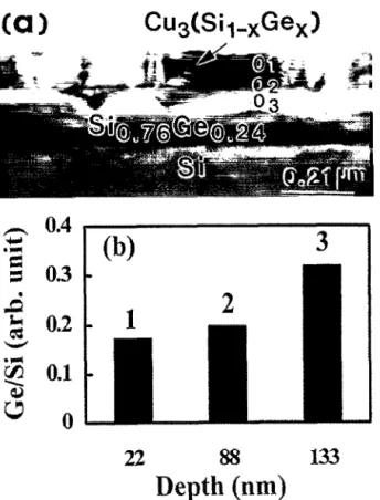
Fig. 1. fa) XTEM image and (b) the depth profile of Ge for the CW Si,, &e,, 24 sample after annealing at 200°C. Ge/Si is the atomic concentra-
tion ratio, x/(1 - x). in the CultSi,-,Ge3 and Si,-,Ge, films.
ber which was kept in a vacuum of approximately 2 X IO-’ Torr { 121. Furnace annealing was carried out in a vacuum of approximately 2.0 x 10e6 Torr. Phase formation and micro- structures were observed by plan-view TEM and cross- sectional TEM (XTEM). The distribution of chemical species in the films was analyzed using EDS which was equipped with a field emission gun with an electron probe 1.2 nm in size. In order to minimize heating during XTEM sample preparation, which could promote the oxidation of
- ~. ..- -.- - .__-
Fig. 2. XTEM image of the Cu/Sil,7hGetilJ sample after annealing-at 25OYZ
23
119
35
24%
Depth
(nm)
Fig. 3. (a) XTEM image and ib) the Gr distribution in the Cu/Si,,&& sample after annealing at 300°C showing Ge segregation out OF &e Cu3iSil-,Ge,z) grains to the surrounding Si,-,Ge,. GelSi is the &%?ic concentration ratio. s/(1 - x), in the CuziSi,-,Ge,) and Si,-,Ge, Rms.
the samples, the epoxy for bonding the sample stack was cured at room-temperature and ion milling of the samples was performed using the substrate holder cooled by liquid N1_.
3. Results and discussion 3.1. Vcicum annealing
For the samples annealed at 200°C T’-Cuj(Sil-,Ge,) was formed from analysis of the electron diffraction pattern. EDSLXTEM analysis showed that the Ge/Si concentration ratio, .x/(1 - x), in the Cuj(Sil-,Ge.J film was reduced, ranging from 0.14 to 0.22 along the film depth, while that in the unreacted Si&ie,J,z4 layer remained unchanged,-i.e. 0.32 as seen in Fig. 1. The reduction of Ge cuncentrationin the germanosilicide was attributed to the capping Si layer ( - 10 nm). During annealing the capping Si layer was involved in the reactions between Cu and Si~~,7bGe,,,14 and hence
.I.S. Lrro et nl. / Tnin Solid Films 346 (19991 207-211 209
ri:a)
-- tSi
f
Cu@
Si0.76Ge0.24
0.21 pm
cb)
oxide
/
31
0.27
pm
Fig. 4. XTEM image of the CU/S~~,.-~~~G~J~~ sample annealed at 2OO’C and followed by exposure in air for (a) 2 and(b) 4 weeks showing that some Cu atoms released from Cul(Sit-,Gc,) by oxidation moved to the Si substrate to form Cu$i and the thickness of the reacted region increased with the exposure time.
diluted the Ge concentration of the germanosilicide. For the samples annealed at 250°C most of the Sio,7hGeo,zl film was consumed and the reacted layer somewhat penetrated to the Si substrate as shown in Fig. 2. From EDYXTEM analysis
oxide
I
Fig. 5. XTEM image of the Cu/Siu,70G~,24 sample annealed at 200°C and followed by exposure in air for 6 weeks showing that the buried SiO2 was initially formed at the Cu3(Si, -,Ge,)/Cu$Si inter-face and subsequently the oxidation of Si proceeded by inward movement of the SiOJSi interface.
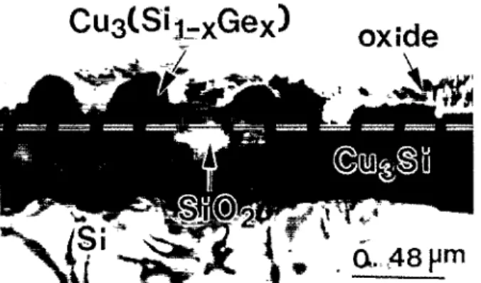
the reacted areas in Si were Ge free, revealing the formation of Cu$i. This result is reasonable since Cu is the dominant moving species in the formation of Cu$i and Cu3Ge by thermal reactions of Cu on Si and Ge. respectively [24,25]. The Ge/Si ratio of the germanosilicide ranged from 0.14 to 0.39 along the film depth. For the samples annealed at 300°C most of the reacted layer penetrated to the Si substrate, forming Cu3(Sil-.YGe,r) and CujSi layers. Meanwhile, agglomeration occurred as shown in Fig. 3; Ge segregated out of the germanosilicide and diffused into the grain boundaries of the germanosilicide to react with Si and Ge from the substrate, forming Ge-rich Sil-,TGe,,. Simi- lar results have been observed in the Ti/Si,-,YGe,Y, Co/ Sil-,,Ge,V, and Ni/Si,-,,Ge,V systems [19,22,26]. The GeLSi ratio of the Cu3(Si,-,1GeY) layer grown at 300°C ranged from 0.05 to 0.24 along the film depth. The heats of forma- tion for Cu$i and CusGe are about -24 and - 16 kJ/mol, respectively [27]. Those values suggest that Cu tends to react preferably with Si.
3.2. Room temnperature oxidation
For the samples annealed at 200°C and then exposed in air for 1 to 4 weeks, an SiO? layer with precipitates containing Cu, Ge, Si, and 0 was formed on the surface of the germa- nosilicide. Both the average thicknesses of the oxide and of the reacted layer increased with the exposure time as shown in Fig. 4. Evidently, after exposure for 2 weeks the reacted layer had already moved to the Si substrate. It has been reported that the Cu atoms released by oxidation of Cu$i move readily to the Cu$i/Si or Si02/Si interfaces to form new Cu,Si [7]. In the present study, the Cu atoms released from Cu3(Si,-,VGe,) by oxidation moved downward to the unreacted Si0.76Ge021 and Si to folm Cu3(Sil-,Ge,) and Cu+Si, respectively.
After exposure for 5-6 weeks, not only the oxidation of the surface layer became severe but also the formation of buried SiOz. was initiated at the Cu~(Sii-,YGe,)/Cu3Si inter- face as shown in Fig. 5. Concurrently, the oxidation of Si proceeding by inward movement of the SiO#i interface was also observed. It is worth noting that voids are usually present in the buried SiO, layer. They may be formed by
Fig. 6. XTEM image of the Cu/Si sample annealed at 200°C and followed by exposure in air for I week.
210 J.S. Luo et al. J Thin Solid Films 346 (1999) 207-211
oxide
Fig. 7. XTEM image of the Cu/SiU.,bGe,,:, sample annealed at 300°C and followed by exposure in air for 1 week.
Ar- milling. For the Cu/Si system annealed at 200°C and followed by exposure in air for I week a buried SiOz layer about 200 nm thick was formed as shown in Fig. 6. No voids were observed in the buried SiO? layer. The buried SiOl layer formed in the Cu/(Sio76-,,Geo,z4) system is not as dense as that formed in the Cu/Si system. Besides, the oxidation rate for the Cu/(Sin,76-.rGe,,,?~) system is evidently lower than that for the Cu/Si system. All these results may be explained in terms of the high stability of Cu3Ge with respect to oxygen [4-6]. Molecular oxygen may be disso- ciated into atomic oxygen in the surface of Cu&, allowing more rapid diffusion through the Cu3Si and SiO; layers [7,9]. The presence of CujGe in the Cu$Si,-,Ge,) film may possibly decrease the diffusion flux of atomic oxygen and Cu through the Cui(Sil-,Ge,J, Cu3Si5 and buried SiOa layers, and hence reduce the Cu&catalyzed oxidation rate. A clear explanation remains to be discovered.
For the Cu/Si system Liu and Chen [12] have reported that the Cu$i-catalyzed oxidation rate decreases with increasing annealing temperature because of grain size effects. In the present study, however, the Cu$i-catalyzed oxidation for the Cu/Siij,76Ge0,2; system was enhanced after higher temperature annealing. One example is shown in Fig. 7. This result is not surprising since after annealing at 250°C some Cu atoms had already moved to the Si substrate to form Cu$i as shown in Fig. 2, eliminating the time required for the release of Cu from Cu&5il-,,Ge,r) by oxidation and the subsequent diffusion of the released Cu to the Si substrate to form new CL@, both of which were involved in the process of room temperature oxidation for the Cuj(Sil-.,Ge,,) films grown at 200°C. Furthermore, the afore- mentioned results have shown that Cu>Ge is stable against oxygen and the formation of buried SiOl is initiated at the Cu&Si, _,Ge.,f/Cu$i interface. In the present study, 300°C annealing yielded the lowest Ge concentration in the Cu$Sil-,YGe,,) layer because of Ge segregation and the largest fraction of the Cu;(Si,-,~Ge,~)/Cu;Si interface as shown in Fig. 3, resulting in the fastest rate of Cu$i-cata- lyzed oxidation.
4, Summary and conclusions
For the Cu/Sill~TbGe,,Z4 sgtiples annealed at 200°C and exposed to air for 1 to 3 weeks. an oxidation layer appeared on the surface of the Cuj(Si,-,Ge,J film. The Cu atoms released from Cuj(Sii -rGe,J by oxidation diffused down to the Si0.7hGei),24 film and the Si substrate to form new Cu7(Si, _,Ge,,) and Cu&, successively. Upon exposure for 5 to 6 weeks, a buried SiOl, layer was initially formed at the Cu3(Si,-,Ge,c)/Cu$i interface; then the oxidation of$i proceeded by inward movement of the SiOJSi interface. The presence of Cu3Ge lowered considerably the oxidation rate of the annealed Cu/Si,-,Ge, samples. Annealing at higher temperatures such as 300°C resulted in (a) Ge sege- gation out of the Cu3(Sii-,Ge,) layer, (b) a larger fraction of the Cu@i,-rGe,,)/Cu$i interface where the buried SiO? layer was initially formed, and (c) an enhanced rate of oxidation catalyzed by Cu$i.
Acknowledgements
This work was sponsored by Republic of China National Science Council under Contract No. NSC86-2215EQW
003. References [II PI [31 Fl PI lb1 [71 181 PI [W t111 WI 1131 1141 1151 [I61 1171 [I81 [I91
H. Miyazaki. K. Hinode. Y. Homma. K. Mtiai. Jpn. J. Appl. Phys. 48 (1987) 329.
J.W. Chen, A.G. Milnes, Annu. Rev. Malei Sci. 10 (1980) i5t~ M.O. Aboelfotoh, A. Cros. B.G. Svensson, K.N. Tu. Phys. Rev. B 41 (1990) 9819.
M.O. Aboelfotoh, L. Krusin-Elbaum. J. Appl. Phys. 70 (1991) 3382. L. Krusin-Elbaum, M.O. Aboelfutoh, Appl. Phys. Lett. 58 (1991) 1341.
M.A. Borek, S. Oktyabrsky, M.O. Aboelfutuh, J. Narayan, Appi. Phys. Lett. 69 (1996) 3560.
J.M.E. Harper, A. Charai, L. Stolt. F.M. d’Heurle, P.M. Fryer, Appl. Phys. Lett. 56 (19901 2519.
M. Setton, J. Van der Spiegel, B. Rothman, Appl. Phys. Lett. 57 (1990) 353* -1
A. Cros, M.D. Aboelfotoh, K.N. Tu. J. Appi. Phys. 67 (1990) 3328. J. Li, J.W. Mayer, L.J. Matienzo, F. Emmi, Mater. C&em. Phys. 32 (1992) 390.
C.S. Liu, L.J. Chen, J. Appl. Phys. 74 11993) 3611. C.S. Liu. L.J. Chen, Thin Solid Films 262 (199.5) 187.
T.L. Alford. E.J. Jaquez, N.D. Theodore, S.W. Russell. M. Diale, D. Adams, S. Anders. J. Appl. Phys. 79 (1996) 1074.
F.Y. Huang, X. Zhu, M.O. Tanner, K.L. Wang, Appl. Phys. Lett. 67 (1995) 566.
R.D. Thompson, K.N. Tu, J. Angillelo, S. Delage, S.S. Iyer, J. Elec- trochem. Sot. 135 (1988) 3161.
Q.Z. Hong. J.W. Mayer, J. Appl. Phys. 66 (1989) 611.
A. Buxbuam. M. Eizenberg, A. Raizm‘an, F. Schafller, Appl. Phys. Lett. 59 (1991) 665.
0. Thomas, S. Delage, F.M. d’Heurle, G. Scilla, Appl. Phys. Lett. 54 119S9) 228.
D.B. Aldrich, FM. d’Heurt, D.E. Sayers, R.J. Nemanich, Phys. Rev. B 53 I19961 16279.
J.S. Luo er al. /Thin Solid Fihzs 346 (1999) 207-211 211 [20] A. Eyal, R. Brener, R. Beserman, M. Eizenberg, 2. Atzmon, D.J. 1241 S.Q. Hong, C.M. Comrie, S.W. Russell, J.W. Mayer, J. Appl. Phys. 70
Smith, J.W. hfayer, Appl. Phys. Lett. 69 (1996) 64. (1991) 3655.
[21] F. Lin, G. Sarcona, M.K. Hatalis, A.F. Cserhati. E. Austin~D.%‘. 1253 L. Stolt, F.M. d’Heurle, Thin Solid Films 189 (1990) 269. @eve, Thin Solid Films 250 (1994) 20. 1261 J.S. Luo. W.T. Lin. C.Y. Chang, W.C. Tsai, J. .4ppl. Phys. 82 (1997)
[22] J.S. Luo, W.T. Lin, C.Y. Chang, W.C. Tsai, S.J. Wang, Mater, Chem. 3621.
Phys. 48 (1997) 140, [27] S.V. Meschel, O.J. Kleppa, Marall. Trans. A 22 (1991) 2162. [23] E.J. Jaquez, A.E. Bair, T.L. Alford, Appl. Phys. Lett. 70 (1997) 874.