Ultrabroadband terahertz field detection by photoconductive antennas based on
multi-energy arsenic-ion-implanted GaAs and semi-insulating GaAs
Tze-An Liu, Masahiko Tani, Makoto Nakajima, Masanori Hangyo, and Ci-Ling Pan
Citation: Applied Physics Letters 83, 1322 (2003); doi: 10.1063/1.1604191 View online: http://dx.doi.org/10.1063/1.1604191
View Table of Contents: http://scitation.aip.org/content/aip/journal/apl/83/7?ver=pdfcov Published by the AIP Publishing
Articles you may be interested in
Terahertz radiation generated and detected by Br + -irradiated In 0.53 Ga 0.47 As photoconductive antenna excited at 800 nm wavelength
Appl. Phys. Lett. 89, 083519 (2006); 10.1063/1.2338538
Terahertz emission properties of arsenic and oxygen ion-implanted GaAs based photoconductive pulsed sources J. Vac. Sci. Technol. A 24, 774 (2006); 10.1116/1.2183284
Generation and detection of ultrabroadband terahertz radiation using photoconductive emitters and receivers Appl. Phys. Lett. 85, 164 (2004); 10.1063/1.1768313
THz radiation emission properties of multienergy arsenic-ion-implanted GaAs and semi-insulating GaAs based photoconductive antennas
J. Appl. Phys. 93, 2996 (2003); 10.1063/1.1541105
Detection of terahertz radiation from longitudinal optical phonon–plasmon coupling modes in InSb film using an ultrabroadband photoconductive antenna
Appl. Phys. Lett. 77, 1798 (2000); 10.1063/1.1311609
This article is copyrighted as indicated in the article. Reuse of AIP content is subject to the terms at: http://scitation.aip.org/termsconditions. Downloaded to IP: 140.113.38.11 On: Thu, 01 May 2014 05:25:30
Ultrabroadband terahertz field detection by photoconductive antennas
based on multi-energy arsenic-ion-implanted GaAs and
semi-insulating GaAs
Tze-An Liu
Institute of Electro-Optical Engineering, National Chiao Tung University, 1001 Ta Hsueh Road, Hsinchu 300, Taiwan, Republic of China
Masahiko Tani, Makoto Nakajima, and Masanori Hangyo
Research Center for Superconductor Photonics, Osaka University, 2-1 Yamadaoka, Suita, Osaka 565-0871, Japan
Ci-Ling Pana)
Institute of Electro-Optical Engineering, National Chiao Tung University, 1001 Ta Hsueh Road, Hsinchu 300, Taiwan, Republic of China
共Received 20 January 2003; accepted 7 July 2003兲
The photoconductive antennas based on multi-energy arsenic-ion-implanted GaAs and semi-insulating GaAs are demonstrated to have a useful bandwidth beyond 20 THz for a gating laser pulse width of 15 fs. The bandwidth and signal-to-noise ratio are compared with those of reference photoconductive antennas based on low-temperature grown GaAs. © 2003 American Institute of Physics. 关DOI: 10.1063/1.1604191兴
Terahertz 共THz兲 time-domain spectroscopy 共THz-TDS兲 based on generation of pulsed THz radiation and its time-domain sampling detection by short laser pulses 共in pump-probe scheme兲 are now widely used as a spectroscopic tech-nique in mm and sub-mm wavelength region. At present, there are two commonly used schemes for generation and detection of THz radiation with femtosecond laser excitation: One is the use of photoconductive 共PC兲 antennas and the other is the use of electro-optic crystals. The useful band-width in the THz-TDS with PC antennas has been typically limited within 3 THz (100 cm⫺1). On the other hand, with the use of thin electro-optic crystals and very short laser pulses less than 20 fs, the spectrum distribution can be ex-tended beyond 30 THz.1,2The limited bandwidth of PC an-tennas was explained by the finite carrier lifetime or the mo-mentum relaxation time of the carriers in the PC substrates. However, recently, Kono, Tani, and Sakai3,4 found that PC antennas based on low-temperature grown GaAs 共LT-GaAs兲 are also able to detect ultrabroadband THz radiation with the use of an appropriate optical setup. They reported the detectable spectral distribution was extended up to 60 THz by using short laser pulses less than 20 fs and a collin-ear geometry for THz beam and probe beam, unlike the com-monly used anti-collinear geometry with the use of Si sub-strate lens.5 The fast response of the PC antennas has been explained by the fast rise of photoconductivity determined by the laser pulse width, while the photoconductive decay is determined by the carrier lifetime, which is much longer than the observed THz field oscillations. However, it was not clear how the photoconductive material properties affect the detection efficiency and bandwidth of PC antennas at such high frequencies. LT-GaAs grown by molecular beam epi-taxy process has properties suitable for the PC antenna
sub-strate, that is, high resistivity, short carrier lifetime and rela-tively good carrier mobility. However, it is not an easy task to fabricate good quality LT-GaAs epitaxial film because op-timization of the growth parameters, such as the growth tem-perature, is required. Arsenic-ion-implanted GaAs (GaAs: As⫹)6exhibits structural, electrical, and ultrafast op-toelectronic characteristics strikingly similar to those of LT-GaAs,7 and is expected to work as an efficient PC sub-strate as LT-GaAs. A semi-insulating 共SI兲 GaAs bulk sub-strate has a good carrier mobility (⬎3000 cm2/V/s), a high dark resistivity (⬃107 ⍀ cm) and a long carrier lifetime (⬎100 ps). It was demonstrated that SI-GaAs can be used as the PC antenna substrate for detection of relatively low fre-quency THz radiation (⬃3 THz),8 although the noise level was significantly high compared to that with LT-GaAs sub-strate.
In this letter, we investigated the effect of substrate prop-erties in the PC detection of ultrabroadband THz radiation by comparing the efficiency and bandwidth of PC antennas made with semi-insulating共SI兲 GaAs, LT-GaAs, and As-ion implanted GaAs. Since these PC materials have different car-rier lifetimes and mobilities, the PC antennas based on these materials were expected to show different detection effi-ciency and bandwidth.
The GaAs: As⫹ substrate was prepared by implanting the semi-insulating 共SI兲 GaAs substrate with arsenic ions at total doses of 1016 ions/cm2 with multiple energies of 50, 100, and 200 keV. This was followed by furnace annealing at 600 °C for 30 min. The ion implantation depth was estimated to be about 100 nm by secondary ion mass spectroscopy measurement. The LT-GaAs was grown at a substrate tem-perature of 250 °C by molecular beam epitaxy and annealed at 600 °C for 5 min after growth. The carrier lifetimes of GaAs:As⫹and LT-GaAs were all estimated to be around 1–2
a兲Electronic mail: [email protected]
APPLIED PHYSICS LETTERS VOLUME 83, NUMBER 7 18 AUGUST 2003
1322
0003-6951/2003/83(7)/1322/3/$20.00 © 2003 American Institute of Physics
This article is copyrighted as indicated in the article. Reuse of AIP content is subject to the terms at: http://scitation.aip.org/termsconditions. Downloaded to IP: 140.113.38.11 On: Thu, 01 May 2014 05:25:30
ps by a transient photoreflectance measurement. A micro-stripline dipole antenna with 30 m dipole length and a 5 m PC gap in the center was fabricated on each PC sub-strate. A mode-locked Ti: sapphire laser, whose pulse width was 15 fs 共the spectral width was 95 nm⬃47 THz), repeti-tion rate 75 MHz, average output power 400 mW, a center wavelength of 800 nm, was used to generate broadband THz radiation from an electro-optic emitter and to gate the PC antenna detector. The experimental setup of the collinear PC detection system,3which is similar to that reported in Ref. 3, was used. The average pump laser power was 150 mW after an optical chopper. Pump beam was focused onto a 10- m-thick共110兲 ZnTe crystal bonded on a 1-mm-thick fused silica plate by a gold-coated off-axis parabolic mirror with a focal length 共f兲 of 50 mm to generate broadband THz radiation by the optical rectification effect. THz beam emitted from the ZnTe emitter was then collimated and focused onto the PC antenna by a pair of off-axis parabolic mirrors ( f⫽50 mm). The gating laser power onto the detector was about 23 mW.
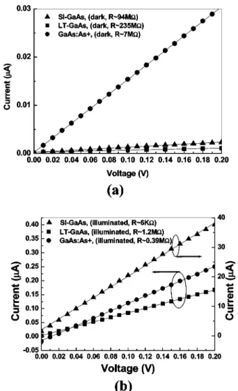
Figure 1 shows the current–voltage (I – V) measurement
共a兲 without and 共b兲 with the laser excitation 共23 mW兲 for the
GaAs:As⫹, LT-GaAs and SI-GaAs PC gap共5m兲 in a weak bias region. SI-GaAs and LT-GaAs PC gaps show lower dark
current. The resistance of LT-GaAs, GaAs:As⫹and SI–GaAs PC gaps decreased to about 1.2 M⍀, 0.4 M⍀, and 6K⍀, respectively, by the laser irradiation. The significant decrease from the high dark resistance (⬃100 M⍀) to the low pho-toconductive resistance共6 k⍀兲 in the SI-GaAs gap indicates a large PC gain, which is attributed to the long carrier life-time. The LT-GaAs gap showed the highest dark resistance. However, its photoconductive resistance was also high共low PC gain兲, which is attributed to the short carrier lifetime (⬃1 ps). On the other hand, GaAs:As⫹ showed the lowest dark resistance, while it showed slightly lower PC resistance
共higher PC gain兲 than that of LT-GaAs 共about one third of
LT-GaAs兲. The lower PC resistance of GaAs:As⫹ compared to that of LT-GaAs is attributed to the slightly longer carrier lifetime (⬃2 ps) and a contribution from the nonion-implanted SI-GaAs substrate, which has a much lower pho-toconductive resistance than the As⫹-ion implanted layer.
There we observed significant stray currents in all anten-nas at the zero bias condition, which may contribute to the noise in THz signal detection; The stray current from SI-GaAs, GaAs:As⫹and LT-GaAs was about 1.5A, 16, and 3 nA, respectively, at the gating power of 23 mW. The origin of the stray currents seems to be the asymmetric Schottky behavior at the metal-semiconductor contact. For dark I – V dependence, such Schottky characteristic is difficult to ob-serve because of relatively high resistivity of the substrate. On the other hand, when we photoexcite the gap with the laser, increasing the conductivity, the Schotty characteristics of the contact become more clear, as observed in the I – V dependence with 23 mW excitation of the PC gap, which showed nonzero crossing at the V⫽0 axis 共the vertical axis兲. Therefore, the high noise level observed in GaAs:As⫹ an-tenna is attributed to the asymmetric Schottky characteristics of the metal-semiconductor contacts in the photoexcited con-dition.
Figure 2 shows the signal wave forms detected by the共a兲 GaAs: As⫹, 共b兲 SI-GaAs and 共c兲 LT-GaAs PC antennas for
FIG. 1. Current–voltage (I – V) measurements共a兲 without and 共b兲 with laser irradiation for GaAs: As⫹ 共circle dot兲, SI-GaAs 共triangular dot兲 and LT-GaAs 共square dot兲 PC gap 共5 m兲 antennas near zero bias region. The resistance共R兲 estimated from the slope is indicated in each diagram.
FIG. 2. Time-resolved THz radiation wave forms detected by PC antenna based on共a兲 GaAs:As⫹,共b兲 SI-GaAs and 共C兲 LT-GaAs. The emitter was a 10-m-thick共110兲 ZnTe crystal.
1323
Appl. Phys. Lett., Vol. 83, No. 7, 18 August 2003 Liuet al.
This article is copyrighted as indicated in the article. Reuse of AIP content is subject to the terms at: http://scitation.aip.org/termsconditions. Downloaded to IP: 140.113.38.11 On: Thu, 01 May 2014 05:25:30
THz radiation generated from the ZnTe emitter. THz wave form detected with the SI-GaAs antenna was averaged for three sequential scanning of the delay stage with a lock-in amplifier time constant of 0.3 s, while for the other PC an-tennas the scanning was only once. The detected peak signal current from GaAs:As⫹, SI GaAs and LT-GaAs PC antennas was 0.02, 0.3, and 0.24 nA, respectively. The signal to noise ratio 共SNR兲 was estimated to be about 20, ⬍10 and 100, respectively. The signal current detected with the GaAs: As⫹ PC antenna was lower than the other two types of PC anten-nas by one order, while the noise level was comparable to that of the LT-GaAs PC antenna. The low signal in the GaAs: As⫹PC antenna is attributed to the insufficient thick-ness of the arsenic ion-implanted layer, which was only 10% of the absorption depth (⬃1m) at the excitation laser wavelength; most of the carriers excited in SI-GaAs substrate beneath the ion-implanted layer could not contribute to the signal since after the photoconductive decay in As⫹-ion-implanted layer, the long-lived carriers in nonion-implanted SI-GaAs are blocked to flow into the antenna con-tact by the insulating layer. The SNR of SI-GaAs PC antenna was lowest, although the signal current level was the highest. The low SNR of SI-GaAs PC antenna is attributed to the large current noise originating from the long-lived photoex-ited carriers (lifetime⬎100 ps), while the other two have carrier lifetimes of 1–2 ps.
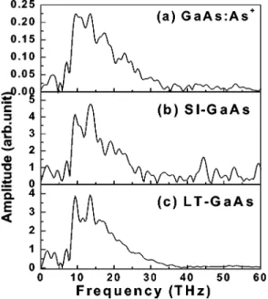
Figure 3 shows Fourier transformed amplitude spectra of
the THz wave forms shown in Fig. 2. The spectrum profiles are almost the same for the three cases. The high frequency end of the spectral distribution is extending to about 30 THz. The end of the spectral distribution above the noise floor was estimated to be 32 and 24 THz for GaAs:As⫹ and SI-GaAs PC antenna, respectively共40 THz for LT-GaAs PC antenna兲, which are the highest frequencies reported so far for the same kind of PC antennas. The spectral bandwidth was lim-ited by the cutoff frequency (⬃40 THz) due to the phase mismatch between共the兲 THz radiation and pump laser pulse in the 10-m-thick ZnTe emitter.3
It was reported that the main contribution to the noise in a PC detector is the Johnson noise共or thermal noise in resis-tance兲 and the laser shot noise.8The Johnson noise in current is inversely proportional to the square root of the resistance, 1/冑R, while the laser shot noise is dependent on the laser power but not on the material properties of the PC substrate. The photoconductive resistance is inversely proportional to the conductivity, , which in turn is proportional to product of mobility,, and carrier life time,. As a result, the noise level is proportional to the square root of the product of carrier lifetime and mobility: Inoise⬀1/冑R⬀冑⬀冑. The
similarity between the spectra obtained with the three types of PC antennas indicates that neither the carrier lifetime nor the mobility共the carrier momentum relaxation time, in other words兲 are critical parameters for the detection bandwidth of the PC antenna, although these material parameters deter-mine the efficiency and noise properties of the PC antennas. In summary, ultrabroadband detection of THz radiation (⬃30 THz) by GaAs:As⫹ and SI-GaAs PC antennas was demonstrated. Their efficiency and bandwidth were com-pared with those of a reference LT-GaAs PC antenna. Al-though the SNR with GaAs:As⫹PC antenna was lower than that of LT-GaAs PC antenna, it is possible to improve the efficiency by increasing the ion-implanted layer thickness. SI-GaAs PC antenna showed poor SNR due to a large noise originating from the long-lived photocarriers.
1Q. Wu and X.-C. Zhang, Appl. Phys. Lett. 71, 1285共1997兲.
2R. Huber, A. Brodschelm, F. Tauser, and A. Leitenstorfer, Appl. Phys. Lett.
76, 3191共2000兲.
3
S. Kono, M. Tani, and K. Sakai, Appl. Phys. Lett. 79, 898共2001兲.
4S. Kono, M. Tani, P. Gu, and K. Sakai, Appl. Phys. Lett. 77, 4104共2000兲. 5S. Kono, M. Tani, and K. Sakai, IEE Proc.-J: Optoelectron. 149, 105
共2002兲.
6F. Ganikhanov, G.-R. Lin, and C.-L. Pan, Appl. Phys. Lett. 67, 3465
共1995兲.
7A. Claverie, F. Namavar, and Z. Liloental-Weber, Appl. Phys. Lett. 62,
1271共1993兲.
8M. Tani, K. Sakai, and H. Mimura, Jpn. J. Appl. Phys., Part 2 36, L1175
共1997兲.
FIG. 3. Fourier transformed amplitude spectra of the PC-detected THz wave forms shown in Fig. 2.
1324 Appl. Phys. Lett., Vol. 83, No. 7, 18 August 2003 Liuet al.
This article is copyrighted as indicated in the article. Reuse of AIP content is subject to the terms at: http://scitation.aip.org/termsconditions. Downloaded to IP: 140.113.38.11 On: Thu, 01 May 2014 05:25:30