國 立 交 通 大 學
顯示科技研究所
碩
士
論
文
在二氧化矽基板上具有小圖形尺寸的
光子晶體奈米結構雷射特性
Laser Emissions from Photonic Crystal Nanostructures with
Small Footprints on SiO
2Substrate
研 究 生:蔡為智
指導教授:李柏璁 教授
在二氧化矽基板上具有小圖形尺寸的
光子晶體奈米結構雷射特性
Laser Emissions from Photonic Crystal Nanostructures with
Small Footprints on SiO
2Substrate
研 究 生:蔡為智 Student:Wei-Chih Tsai
指導教授:李柏璁 博士 Advisor:Dr. Po-Tsung Lee
國 立 交 通 大 學
顯示科技研究所
碩 士 論 文
A Thesis
Submitted to Department of Photonic and Display Institute College of Electrical Engineering and Computer Science
National Chiao Tung University In partial Fulfillment of the Requirements
for the Degree of Master in
Electro-Optical Engineering September 2012
Hsinchu, Taiwan, Republic of China
中華民國 101 年 8 月
I
在二氧化矽基板上具有小圖形尺寸的
光子晶體奈米結構雷射特性
研究生:蔡為智 指導教授:李柏璁 博士 國立交通大學顯示科技研究所 摘 要 在二氧化矽基板上具有小圖形尺寸的光子晶體雷射不僅具有結構穩定的特性,更適 合整合於積體光路中做為光源元件。而透過三五族材料整合於矽基材料上的奈米結構, 更被視為矽奈米光學中有效發光元件的解決方案之一。 在 本 論 文 中 , 透 過 兩 種 光 子 晶 體 加 強 光 - 物 質 交 互 作 用 的 機 制 , 輔 以 DVS-bis-Benzocyclobutene 黏著接合技術,我們在二氧化矽基板上實現具有小圖形尺寸 的光子晶體雷射元件。第一種方式是利用晶格對稱點附近具有極小群速度的光子平帶。 基於此機制,我們透過二維正方晶格光子晶體中 M 對稱點的平帶來實現在二氧化矽基 板上的帶緣雷射,並做為後續的對照組。接著,藉由消除一個方向的光子晶體,我們在 二氧化矽基板上進一步地實現一維光子晶體奈米樑帶緣雷射,其展現出來的元件尺寸以 及雷射閥值皆比二維正方晶格光子晶體帶緣雷射來的小。第二種方式則是以形成共振腔 來加強光-物質交互作用。基於此機制,我們利用封閉一維光子晶體奈米樑的概念來形 成一種新穎的一維光子晶體環形共振腔,在實驗上所展現出來的元件圖形尺寸只有 30 μm2,且其環形直徑僅有 3.56 μm。而在實驗上最小能夠觀察到雷射行為的環形直徑僅 3 μm。此外,我們進一步地在一維光子晶體環形結構中設計具有模隙侷限效應的奈米共 振腔。相較於一維光子晶體環形共振腔,我們從此種雷射元件可取得較小的模態體積以 及較低的雷射閥值。除了極小的元件圖形尺寸外,此類環形光子晶體共振腔可透過側向 光波導耦合的方式,在整合於積體光路時,在耦合機制上展現絕佳的可變化性。II
Laser Emissions from Photonic Crystal Nanostructures with
Small Footprints on SiO
2Substrate
Student: Wei-Chih Tsai
Advisor: Dr. Po-Tsung Lee
Display Institute,
National Chiao Tung University
Abstract (English
Abstract
Photonic crystal (PhC) lasers with small device footprint on silicon-dioxide (SiO2)
substrate not only has mechanically stable property but also is a good candidate for light sources in condensed photonic integrated circuits (PICs). Moreover, III-V active materials on silicon-based substrate are regard as a feasible solution of efficient light sources in silicon photonics.
In this thesis, based on two different mechanisms for enhancing light-matter interactions, DVS-bis-Benzocyclobutene adhesive bonding is utilized to realize ultra-compact PhC lasers on SiO2. The first method is using the flat photonic bands with very low group velocities near
the highly symmetric points of PhCs. Via this mechanism, two dimensional (2D) square-PhC band-edge (BE) lasers at M symmetric point are demonstrated for reference. Via eliminating the PhCs in one dimension, we further demonstrate one-dimensional (1D) PhC nanobeam (NB) BE lasers on SiO2 substrate. Such devices not only have smaller device footprints but
also lower threshold value than those of 2D-square PhC BE lasers. The second method is forming resonators to enhance light-matter interactions. Via this mechanism, we propose and realize a novel 1D PhC ring resonator (PhCRR) on SiO2, a design formed by encircling 1D
PhC NB. This kind of device also shows small device footprint of 30 μm2. The minimum ring diameter for lasing in experiments is 3 μm. Furthermore, we also design a mode-gap confined nanocavity on 1D PhCR. Smaller mode volume and lower lasing threshold than those of 1D
PhCRRs are obtained. In addition to small device footprints, lasers based on PhCRs also show
III
Acknowledgements
兩年碩士生涯倏忽即逝,在這艱辛的道路上,首先我要感謝我的指導教授 李柏璁 博士在研究上給予的指導。此外,老師對排球的熱情也帶給了全實驗室的人。我想這共 同的課外活動使得我們實驗室更顯獨特,也更有凝聚力。謝謝老師。 再者我要感謝 盧贊文大學長,學長在實驗上的討論及精闢的見解讓我少走許多冤 枉路。同時,在論文的寫作以及投影片的製作上給予的寶貴意見都讓我受益良多。雖然 做為學長在此實驗室的閉門弟子,有太多時候沒能符合學長的期望,但學長總是願意花 時間指點我,讓我更有效率的做好我的研究。另外要謝謝 林品佐學長不僅願意在研究 上提供協助,也願意分享到許多研究以外的知識,讓我的研究所生涯更顯豐富。同為 Photonic Technology Lab 的一份子,謝謝 哲嶢、宜錩在 E-beam 以及 SEM 上 的幫忙。謝謝 學弟恆沂在實驗後期提供的協助,讓我能無後顧之憂的專注實驗上的量 測,以後你可要好好的對待ICP。謝謝 家揚學長、開昊讓我知道許多表面電漿的知識。 謝謝太陽能組的各位: 光揚學長、品睿學姐、佳裕學長、權政、佑政在 SRO 的題目上 所提供的協助,雖然在此題目上沒能有太大的進展,但是各位在機台以及量測上所提供 的協助,都讓我壓力減輕不少。謝謝已經畢業的學長姐們: 邱立勛、林雋威、呂紹平、 許書維、莊文齡在我剛進實驗室時,帶領我熟悉實驗室,熟悉新竹的環境。 特別感謝 交通大學 陳方中實驗室以及 中央大學 許晉瑋實驗室在實驗器材以及 材料上提供的協助,讓此研究得以順利進行。感謝 交通大學電子所的 張家豪學長在 ICP 機台管理上的指導。如果沒有學長的指導,我未必能夠順利解決每一次的 alarm。 感謝 中央大學 陳志強教授在我大學時教過我的任何知識。謝謝大學同學 許鈞筌、 陳立人、陳韋先、黃雨平還有高中同學 張博超、張晏豪、陳文傑、陳干越、李佑軒、 范國強,雖然你們都很白目,但在我情緒低落、需要人傾聽時你們絕對是很好的朋友。 謝謝我從小的好朋友 夏佑賢總是告訴我許多有趣的事情,希望未來你的學生生涯能夠 順利。 謝謝我最親愛的家人,總在我需要你們的時候能夠提供慰藉,讓我不致崩潰。 最後,謹以此論文獻給愛我但沒能看到我畢業的外婆及姑姑。 蔡為智 2012 年 9 月 謹誌於 新竹交通大學 交映樓
IV
Table of Contents
Abstract (Chinese)……….………..I Abstract (English) ... II Acknowledgements ... III Table of Contents ... IV Table Captions ... VII Figures Captions ... VIIIChapter 1 ... 1
Introduction ... 1
1.1 Photonic Crystal Lasers ... 1
1.2 Footprint Minimization of PhC Lasers ... 3
1.3 Compact PhC Lasers on Asymmetric Structure ... 5
1.4 Motivation and Proposed Structures ... 6
1.5 Thesis Overview ... 7
Chapter 2 ... 8
Simulation Methods, Fabrication Processes, and ... 8
the Measurement System ... 8
2.1 Introduction ... 8
2.2 Numerical Simulation Methods for Photonic Crystal ... 8
2.2.1 Plane-Wave-Expansion Method ... 10
2.2.2 Finite-Element Method ... 11
2.2.3 Simulation of Photonic Crystal Device ... 13
2.3 Fabrication Process of PhC (III-V Materials) Nano-Structue on SiO2 ... 14
2.3.1 Transferring MQWs on SiO2/Si Substrate via Adhesive Bonding ... 15
V
2.3.3.1 Depositing SiNx Hard Mask and Defining PhC Patterns ... 19
2.3.3.2 Transferring PhC Patterns via Dry Etching Process ... 20
2.4 Measurement Setup ... 22
2.5 Demonstration of Microdisk Laser on SiO2/Si substrate ... 23
2.6 Summary ... 24
Chapter 3 ... 25
Photonic Crystal Band-Edge Lasers ... 25
on SiO2 Substrate ... 25
3.1 Introduction ... 25
3.2 Optical Properties of 2D Square-PhC BE Lasers on SiO2 Substrate ... 25
3.3 1D PhC NB BE Lasers on SiO2 Substrate ... 29
3.3.1 Modal Properties of Dielectric Band in Simulations ... 30
3.3.2 1D PhC NB BE Lasers on SiO2 Substrate ... 32
3.4 Summary ... 37
Chapter 4 ... 38
1D Photonic Crystal Lasers ... 38
Based on Ring Resonator on SiO2 Substrate ... 38
4.1 Introduction ... 38
4.2 1D PhCRR Lasers on SiO2 Substrate ... 39
4.2.1 Dielectric Mode Properties in 1D PhCRR ... 39
4.2.2 Measurement Results of 1D PhCRR Lasers on SiO2Substrate ... 41
4.3 Mode-Gap Confined Nanocavity Lasers in 1D PhCR on SiO2 Substrate ... 45
4.3.1 Design of Mode-Gap Confined Nanocavity in 1D PhCRR ... 46
4.3.2 Lasing from 1D PhCR-nc on SiO2 Substrate ... 46
4.4 Summary ... 48
VI
Summary and Future Works ... 50
5.1 Summary ... 50
5.2 Future Works ... 51
Appendix A ... 52
A.1 Device Footprints of Photonic Crystal Devices ... 52
References ... 53
VII
Table Captions
Chapter 2
Table 2-1: Average thickness of the BCB layer under different spin-coating conditions. ... 17 Table 2-2: SiNx hard mask deposition condition via PECVD. ... 19
Table 2-3: Recipe of RIE and ICP mode. ... 21
Chapter 3
VIII
Figures Captions
Chapter 1
Fig. 1-1: Schemes of 1D, 2D, and 3D PhCs and the corresponding pictures. ... 1 Fig. 1-2: Scheme of photon manipulations in a 2D PhC slab. ... 2 Fig. 1-3: (a) Scheme of a 2D PhC single-defect nanocavity and its confinement mechanism. (b) Band diagram and BE mode profile in magnetic field at M1 point in 2D hexagonal-PhC slab. 2
Fig. 1-4: (a) Optical confinement mechanism and (b) SEM picture of 1D PhC Si NB on SiO2
substrate [21]. ... 4 Fig. 1-5: SEM pictures and mode profiles of 1D PhC NB nanocavities with (a) parabolic beam width modulation [23] and (b) effective index matching [24]. (c) 1D PhC NB BE laser [26]. .. 4 Fig. 1-6: Schematic of 1D PhC NB (III-V material) on low index SiO2 substrate via BCB
bonding technique. ... 6 Fig. 1-7: (a) Scheme of 1D PhCRR formed by an encircled 1D PhC NB on SiO2. Micro-disks
with different circular periodic nanostructure arrangement: (b) grating [45] and air holes [46]. ... 7
Chapter 2
Fig. 2-1: Scheme of the tetrahedral element in FEM. ... 11 Fig. 2-2: (a) Scheme of 1D PhC NB and its (b) propagating band diagram via PWE method. (c) The mode profiles in Ey field of the first three bands at k = 0.5. ... 13
Fig. 2-3: Theoretical Q factor of the dielectric bandedge mode as a function of NB (a) length and (b) width via 3D FEM. ... 14 Fig. 2-4: Schematic of PhC structure on III-V active material (InGaAsP MQWs) with underlying low index SiO2 on Si substrate. ... 15
Fig. 2-5: (a) Epitaxial structure of InGaAsP MQWs on InP substrate and (b) it PL spectrum with peak wavelength near 1540 nm. (c) Picture of PECVD, facilities of Center for Nano-Science Technology (CNST), National Chiao Tung University (NCTU). ... 16 Fig. 2-6: The flow chart of transferring InGaAsP MQWs onto SiO2 substrate. ... 16
IX
Fig. 2-7: (a) Average thickness of the BCB layer under spin coating condition 3 and different diluted ratios shown in Table 2-1. The corresponding cross-section SEM pictures are also shown as the insets. (b) PL spectrum and picture (inset) of InGaAsP MQWs on SiO2/Si substrate
after BCB bonding process. ... 17 Fig. 2-8: The flow chart of realizing PhC structures on the MQWs on SiO2/Si substrate via BCB
adhesive bonding. ... 18 Fig. 2-9: The measured PL spectrum and picture (inset) of MQWs after depositing SiNx. ... 19
Fig. 2-10: (a) EBL system (ELS - 7500EX), facilities of CNST, NCTU. (b) Top-view SEM picture of defined 2D PhCs on PMMA. ... 20 Fig. 2-11: (a) RIE-ICP system, facilities of CNST, NCTU. (b) SEM picture of transferred PhCs on SiNx hard mask. (c) The measured PL spectrum of MQWs after transferring the PhC patterns
into SiNx via RIE. ... 20
Fig. 2-12: (a) The measured PL spectrum of MQWs after transferring PhC pattern into MQWs via ICP dry etching. (b) Top- and tilted-view SEM pictures of a square-PhCs on SiO2/Si
substrate. ... 21 Fig. 2-13: Flow chart of fabricating PhC nano-structures on MQWs on SiO2/Si substrate. ... 22
Fig. 2-14: Schematic of the NIR confocal micro-PL measurement system... 23 Fig. 2-15: (a) Scheme of a microdisk on SiO2/Si substrate. (b) Top-view SEM picture and (c)
single mode lasing spectrum at 1538.2 nm of a microdisk with 3.56 μm in diameter on SiO2/Si
substrate. Theoretical lasing WG mode profile in electric field with azimuthal number of 15 via
3D FEM is shown as the inset of (c). ... 24
Chapter 3
Fig. 3-1: (a) Scheme and top-view SEM pictures of 2D square-PhCs on SiO2 substrate. (b) The
photonic band diagram of 2D square-PhCs with r/a = 0.22 and t = 200 nm on SiO2 substrate
via 3D PWE method. The gain region of InGaAsP MQWs is denoted by the red shadow. (c) Simulated electric field distribution of X0, X1, M0, and M1 BE modes by 3D FEM. (d)
Theoretical Q factors of X0, X1, M0, and M1 BE modes in 2D square-PhC on SiO2 under different
X
Fig. 3-2: (a) Measured lasing spectrum in dB scale with lasing wavelength at 1578 nm and
SMSR of 30 dB from 2D square-PhC BE laser on SiO2. (b) L-L curve of 2D square-PhC BE
laser on SiO2 shows threshold power of 4.25 mW. The inset shows the lasing spectra under
different pump power. (c) Lasing spectra from 2D square-PhC on SiO2 under different r/a
ratios and the measured lasing frequencies and simulated M1 mode frequency under different
r/a ratio of 2D square-PhC BE laser on SiO2. (d) The measured polarization with polarized
ratio of 1.8. The simulated Ex and Ey fields of M1 BE mode is also shown as the insets. ... 27
Fig. 3-3: (a) Scheme and important parameters of 1D PhC NB on SiO2 substrate. (b) Photonic
band diagram of 1D PhC NB on SiO2 substrate via 3D PWE. The mode profiles in Ey fields of
the first three bands at kx = 0.5 are also shown as the inset. ... 29
Fig. 3-4: Theoretical (a) wavelength, (b) Q, and V of the dielectric mode as a function of P in 1D
PhC NB on SiO2. ... 30
Fig. 3-5: Theoretical Q and V as a function of (a) beam width w (with fixed r/a = 0.35) and (b)
r/a ratio (with fixed w = 1.3a), while t, a, and P are fixed at 200 nm, 400nm, and 28 respectively.
... 31 Fig. 3-6: Top- and tilted-view SEM pictures of 1D PhC NB with P of 28 on SiO2 substrate... 32
Fig. 3-7: (a) 1D PhC NB on SiO2 substrate with directly defined air-windows shows significant
distortion in NB shape. Theoretical mode profile in electric fields of dielectric mode in 1D PhC
NB on SiO2 (a) without DBRs, (b) with ideal DBRs for 1550 nm, and (c) with DBRs with
parameters in fabrications. The parameters t, r/a, w, and P of 1D PhC NB are 180 nm, 0.28, 1.31a, and 28. Theoretical wavelengths and Q factors of the three situations are almost the same. ... 33 Fig. 3-8: Measured single-mode lasing spectrum at 1486 nm shows SMSR > 25 dB under pump power of 7 mW. (b) The measured emission shows linear polarization with polarized ratio of 10.9, owing to the dominated Ey field of the dielectric mode in 1D PhC NB, as shown by the
insets. ... 33 Fig. 3-9: (a) A threshold power of 0.78 mW is obtained from the L-L curve. The inset shows the lasing spectra under different pump power to confirm the single-mode lasing. (b) Wavelength matching between the measurement and 3D FEM simulation results of the dielectric mode in 1D PhC NB BE lasers with fixed t, a, and r/a ratio of 200 nm, 400 nm, and 0.31 under different w. ... 34
XI
Fig. 3-10: (a) SEM picture of 1D PhC NB BE laser on SiO2 and scheme of pump spot shifting. (b)
Normalized laser emission intensities under different pump spot position from the center of NB along x- and y-directions. (c) Theoretical mode profile in electric field of the dielectric BE mode in 1D PhC NB and its extended electric field distribution along the cross-line of the NB in
x-direction. ... 35
Fig. 3-11: (a) Top-view SEM picture, (b) single-mode lasing spectrum, and (c) L-L curve of 1D
PhC NB BE laser with P = 36. The L-L curve shows a low threshold power of 0.6 mW. The
parameters t, w, a, and r/a ratio are 200 nm, 1.39a, 400 nm, and 0.29 respectively. ... 37
Chapter 4
Fig. 4-1: (a) Scheme of 1D PhCRR on SiO2 substrate and (b) definitions of important
parameters. (c) Theoretical mode profile in electric field of 1D PhCRR with P = 28 via 3D FEM. ... 39 Fig. 4-2: (a) Theoretical Q and γd factors of 1D PhCRR as a function of P form 10 to 50 with
fixed w and r/a ratio of 1.3a and 0.28. (b) Theoretical Q and γd factors as a function of w with
fixed P and r/a ratio of 28 and 0.28. (c) Theoretical Q and γd factors of 1D PhCRR as a function
of r/a ratio with fixed P and w of 28, and 1.3a. The parameters t and a are fixed at 190 and 400 nm in (a)-(c). ... 40 Fig. 4-3: (a) Top- and (b) tilted-view SEM pictures of 1D PhCRR with P = 28. Underlying SiO2
substrate can be clearly observed in (b). Theoretical mode profiles in electric fields of 1D
PhCRR (c) without DBRs, (d) with ideal DBRs for 1550 nm, and (e) with DBRs in fabrications.
The parameters t, r/a ratio, w, and P of 1D PhCRR are 160 nm, 0.25, 550 nm, and 28. The theoretical wavelengths and Q factors of 1D PhCRRs in (c)-(e) are denoted and almost the same. ... 42 Fig. 4-4: (a) Single mode lasing spectrum from 1D PhCRR on SiO2 substrate with lasing
wavelength of 1523 nm and SMSR of 26 dB. (b) The L-L curve and the inset polarization show a threshold power of 0.7 mW and low polarized degree of 1.94. Theoretical and measured lasing wavelengths of 1D PhCRR with (c) different w and (d) r/a ratios on SiO2. ... 43
Fig. 4-5: (a) The measured lasing wavelength from 1D PhCRRs on SiO2 with different P. Lasing
action can be still observed when P = 24. (b) Single-mode lasing spectrum and SEM picture of
1D PhCRR on SiO2 with P = 24. (c) The 0th- and 1st-order modes can be observed in spectrum
simultaneously when P increases to be 36. The measured wavelength difference is 8.1 nm. (d) Theoretical mode profiles in electric fields of the 0th- and 1st-order modes. The theoretical wavelength difference is 9.2 nm. ... 44
XII
Fig. 4-6: (a) Illustration of mode-gap confinement mechanism via 1D PhC NBs with different
r/a ratios. (b) Mode-gap confined 1D PhCR-nc is achieved by continuously tuning the air-hole
radii. (c) Theoretical mode profile in electric field of the confined dielectric mode in 1D
PhCR-nc. ... 45
Fig. 4-7: Top-view SEM pictures of 1D PhCR-nc with P = 28. The air-hole radii inside (r0) and
outside (r4) the nanocavity region are also shown as the inset SEM pictures. ... 47
Fig. 4-8: (a) The measured lasing spectrum with lasing wavelength of 1535 nm. The inset shows SMSR of 28 dB. (b) The L-L curve shows threshold value of 0.54 mW. The inset shows the measured emission with x-polarized ratio of 3.19. Theoretical and measured lasing wavelengths of 1D PhCR-nc with (c) different w and (d) r0/a ratios on SiO2. ... 47
Fig. 4-9: The measured thresholds of 1D (a) PhCRRs and (b) PhCR-ncs under different w and
r/a. ... 48
Appendix A
Fig. A-1: Definitions of device footprints of (a) 2D square-PhCs, (b) 1D PhC NB, and (c) 1D
1
Chapter 1
Introduction
1.1 Photonic Crystal Lasers
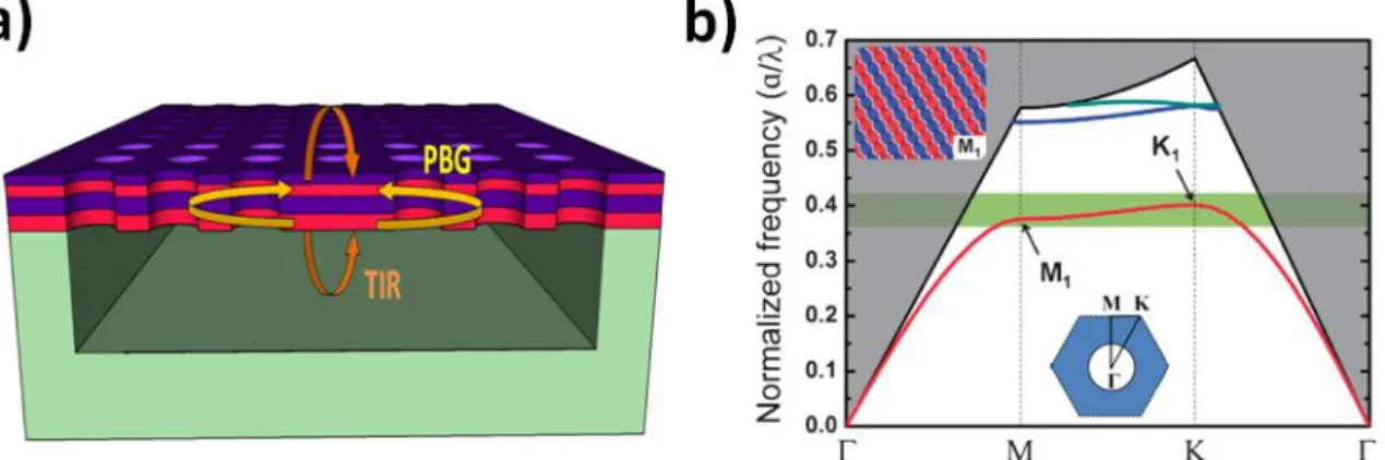
Electron manipulation can be achieved in electronic devices by means of electronic band structure in semiconductor materials. This electronic band structure is origin from the superposition of periodic atomic potentials. Similar to electronic band, photonic band can also be induced in a structure named as photonic crystal (PhC) with periodic refractive index arrangement. In 1987, two milestone ideas of PhCs were proposed by E. Yablonovitch [1] and S. John [2] for spontaneous emission inhibition and photon restriction. Controllable photonic band diagram and photonic band gap (PBG) are the fascinating properties of PhCs, which realize the manipulation of photons in wavelength scale. According to periodic dimensions,
PhCs can be classified into one- (1D), two- (2D) and three-dimensional (3D) PhCs, as shown
in Fig. 1-1. Among these PhCs, 2D PhCs have been widely realized on a suspended slab with finite thickness, as shown in Fig. 1-2, owing to the easiness and feasibility in fabrication. In this structure, with total internal reflection (TIR) confinement in vertical direction, the photon manipulations by PhCs are available in in-plane directions. Via photonic band engineering or precisely-designed defects, controlling photons in wavelength scale realizes 2D PhC slab
2
Fig. 1-2: Scheme of photon manipulations in a 2D PhC slab.
devices with various functions in recent years, for example, optical filters [3,4], optical memory and logic devices [5,6], light emitter sources, and so on [7-9].
Among these applications, PhC laser shows excellent properties as a light source in photonic integrate circuits (PICs). Generally, there are two main approaches in different PhC structures for lasing. The first one is designing a defect in 2D PhCs to form a resonator via
PBG effect [10], for example, a 2D PhC single-defect nanocavity shown in Fig. 1-3(a). The
defect can be the size, position, or dielectric constant mismatch of one to several cells in
Fig. 1-3: (a) Scheme of a 2D PhC single-defect nanocavity and its confinement mechanism. (b) Band diagram and BE mode profile in magnetic field at M1 point in 2D hexagonal-PhC
3
PhCs. Then the photons will be confined and recycle inside the defect, thus enhances the
light-matter interaction and reach lasing.
The other approach is enhancing optical gain via the slow light effect and interference between lattices near the edge of the Brillouin zone [11], that is, at high symmetric points, in a defect-free PhC slab. At these high symmetric points, the photonic bands become flat, which means the group velocities (vg = δω/δk) approach zero. The nearly zero group velocity leads
to increase of the optical path and time of light-matter interaction, which mainly contributes to lasing. These modes operating at the edge of Brillouin zone are called PhC band-edge (BE) modes. A typical band diagram of 2D hexagonal-PhC slab and the BE mode profile in magnetic field at M1 point are shown in Fig. 1-3(b). Moreover, because there is no local and
delicate defect design, this type of PhC laser can be fabricated via relatively high throughput fabrication process than using electron beam lithography, for example, laser holography [12], nano-imprint [13], nano-sphere lithography [14], and so on.
In recent years, various lasers with excellent properties have been proposed and demonstrated based on 2D PhC slabs [14-18]. However, while maintaining various excellent optical properties in wavelength scale, 2D PhCs also lead to too large device footprint for constructing condensed PICs. In 2008, E. Kuramochi et al. tried to partially remove the 2D
PhC periods to reduce the device footprint [19]. However, without sacrificing the devices
performances, greatly reducing the footprint in 2D PhCs system is still challenging [20].
1.2 Footprint Minimization of PhC Lasers
To break through the bottleneck in minimizing device footprint, 1D PhC nanobeam (NB) will be a feasible solution. This structure was firstly proposed by J. S. Foresi et al. in 1997 [21], which is consisted of air holes penetrate into silicon (Si) waveguide on silicon-dioxide
(SiO2) substrate, as shown in Fig. 1-4(a) and (b). The photon is confined inside a single defect
4
Fig. 1-4: (a) Optical confinement mechanism and (b) SEM picture of 1D PhC Si NB on SiO2
substrate [21].
designed cavity was still lossy on that time. Fortunately, owing to the mature of low-loss nanocavity design principle [22], very recently, versatile 1D PhC NB devices have been proposed and demonstrated with very small device footprints, including laser light sources [23-26], optical sensing [27], optical manipulation [28], optomechanics [29], and so on.
As the laser light sources, up to date, most demonstrations are based on slab structures. For example, B. H. Ahn et al. have demonstrated 1D PhC NB lasers via mode gap
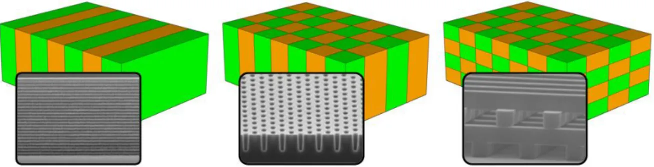
Fig. 1-5: SEM pictures and mode profiles of 1D PhC NB nanocavities with (a) parabolic beam width modulation [23] and (b) effective index matching [24]. (c) 1D PhC NB BE laser [26].
5
confinement with parabolic beam width modulation [23], as shown in Fig. 1-5(a). Y. Gong et
al. [24] and Y. Zhang et al. [25] have demonstrated 1D PhC NB lasers via continuous
effective index modulation, as shown in Fig. 1-5(b). In addition, very recently, the 1D PhC
NB BE laser [26] is also reported by Prof. Y. H. Lee in KAIST, Korea, as shown in Fig. 1-5(c).
Although the slab structure provides good optical confinements, the single-log bridge-like structure also shows mechanical instability and may result in structural collapse [30].
1.3 Compact PhC Lasers on Asymmetric Structure
To provide mechanically stable supporting for the fragile 1D PhC NB structures without resulting in huge optical loss, a low refractive index substrate inducing beneath the PhC NB can meet the requirements simultaneously. And SiO2 material will be a good candidate not
only because of its low index (~ 1.44), but also owing to its good thermal conductivity and low cost.
There have been several widely-used approaches for integrating III-V active material onto Si-based substrates. The first one is flip-chip integration, which is the most matured technique [31]. In this package level technique, the completed components are flipped and bonded onto Si-based substrate. The disadvantage is time consuming due to the alignment issue. The second one is epitaxial growth of III-V material on Si-based substrates. However, the lattice mismatch between III-V material and Si results in high density of defects, and degrades the performance of the devices [32]. The third one is bonding technique. This technique not only provides high quality bonding interface, but also allows the following devices fabrication process, which can avoid alignment issue. Recently, various bonding strategies have been demonstrated, including SiO2-SiO2 direct bonding [33], Au/In eutectic
bonding [34], spin-on-glass [35], and DVS-bis-Benzocyclobutene (BCB) bonding [36-39]. Among these approaches, BCB bonding technique shows high reliability and convenience in
6
Fig. 1-6: Schematic of 1D PhC NB (III-V material) on low index SiO2 substrate via BCB
bonding technique.
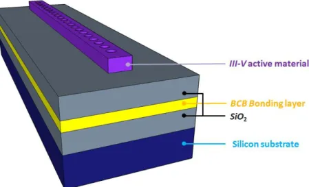
fabrication process. Therefore, BCB bonding technique is used for realizing the PhC active (III-V material) laser devices with underlying low index SiO2 substrate in this thesis. Scheme
of 1D PhC NB with underlying low index SiO2 via bonding technique is shown in Fig. 1-6.
1.4 Motivation and Proposed Structures
To summarize, in this thesis, we want to design and demonstrate PhC lasers with ultrasmall footprint and mechanically stable structure. To reach this goal, bonding techniques for integrating III-V materials on Si-based substrate is applied to realize the structure of 1D
PhC NB on SiO2 substrate. At first, we demonstrate a 2D square-PhC BE laser on SiO2 for
reference. And then the device is transformed into a 1D PhC NB BE laser via eliminating
PhCs in one dimension. Although S. Kim et al. have proposed 1D PhC BE laser based on slab
structure [26], 1D PhC NB BE laser on SiO2 has not been demonstrated yet.
Based on 1D PhC NB BE laser on SiO2, we further encircle the NB to form a novel 1D
PhC ring resonator (PhCRRs) that only can be realized in structure with underlying substrate,
as shown in Fig. 1-7(a). PhCRRs have been widely developed in 2D PhC system and applied in various functional devices for PICs, such as efficient lasers [40, 41], add-drop filters [42], logical gates [43], optical buffers [44], and so on. However, comparing with 2D PhCRRs, 1D
7
Fig. 1-7: (a) Scheme of 1D PhCRR formed by an encircled 1D PhC NB on SiO2. Micro-disks
with different circular periodic nanostructure arrangement: (b) grating [45] and air holes [46].
PhCRR not only shows much smaller device footprint, but also has higher flexibilities in
coupling scheme via side-coupled ridge waveguides in PICs owing to absence of lattice structure restrictions. In addition, unlike the micro-disks with different surrounded periodic designs [45, 46] in Fig. 1-7(b) and(c), only a high Q mode can reach lasing in 1D PhCRR. Based on 1D PhC ring structure, we also design a mode-gap confined nanocavity for lasers with lower thresholds and smaller mode volumes.
1.5 Thesis Overview
The organization of this thesis is illustrated as the following. In chapter 2, fabrication techniques of realizing compact PhC lasers on SiO2 will be introduced in details, especially in
BCB adhesive bonding for integrating III-V material on SiO2 substrate. The simulation
methods (Plane-wave expansion and finite-element methods) and measurement setup for designing and analyzing the devices will also be introduced. In chapter 3, 2D square-PhC and
1D PhC BE lasers on SiO2 substrate are demonstrated. The modal properties will be
investigated both in simulations and experiments. Then in chapter 4, we will propose, demonstrate and discuss the lasing emission from 1D PhCRRs and 1D PhC rings with mode-gap confined nanocavities. Finally, in chapter 5, we will summarize our present and future works.
8
Chapter 2
Simulation Methods, Fabrication Processes, and
the Measurement System
2.1 Introduction
In this chapter, we will give a briefly introduce to our numerical methods, fabrication processes, and the measurement system for photonic crystal (PhC) light emitting devices. In section 2.2, the plane-wave expansion (PWE) and the finite-element methods (FEM) will be introduced, which can be utilized for calculating band diagram and modal properties of various PhC structures. In section 2.3, fabrication processes of forming PhC devices on silicon-dioxide (SiO2) substrate will be illustrated. In section 2.4, we will introduce the
near-infrared (NIR) micro-photoluminescence (micro-PL) system used for measuring the emissions from PhC devices.
2.2 Numerical Simulation Methods for Photonic Crystal
Light propagation in periodic dielectric medium (PhCs) can be illustrated by the four Maxwell equations in MKS unit:
(2-1)
(2-2)
(2-3) (2-4)
where the , , , , ρ, are the magnetic flux density, electric displacement, electric fields, magnetic fields, free charges, and current densities. In addition, there are some restrictions in our dielectric medium. The dielectric material should be: (1) Source free material: ρ and are both set to zero. (2) Isotropic material: the terms of and
9
are related by multiplying the term of , where , are permittivity in free space and relative permittivity. And the term of is a spatial periodic dielectric function and determined by the different PhC structures. (3) Transparent material: the term of can be treated as positive and real. (4) Non-magnetic material: the term of , where is permeability in free space. (5) Frequency independent material. With all of these restrictions, the Maxwell equations (2-1) – (2-4) can be simplified and became as following equations:
(2-5) (2-6) (2-7) (2-8)
Solutions in electric and magnetic fields are harmonic functions, and can be expressed as the product of spatial and time function separately. The terms of and can be written as the following equations:
(2-9)
(2-10)
By substituting equations (2-9) and (2-10), original equations (2-5) – (2-8) will become: (2-11)
(2-12)
(2-13) (2-14)
The terms of and are correlated in equations (2-13) and (2-14). We can get the master equation only relate to by decoupling these two equations:
10
(2-15)
where is the vacuum speed of light. Therefore, we can solve (2-15) to find modes at certain frequency for different PhC structures.
In the following sections, we will introduce two numerical simulation methods that for analyzing the PhC structures, including plane-wave expansion (PWE) and finite-element methods (FEM).
2.2.1
Plane-Wave-Expansion Method
PWE method is an efficiency and useful way to obtain the dispersion relation of a given PhC structure. According to the Bloch theorem, eigen-function in a periodic system can be
expressed as the product of periodic function and plane-wave envelope function. The main idea of PWE simulation is expressing the dielectric function and periodic function in Bloch function as Fourier expansion:
(2-16)
(2-17)
where vector is reciprocal lattice vector. The Fourier coefficient,
and Vc is the volume of the unit cell. By substituting equations
(2-16) and (2-17) into master equation (2-15), the master equation becomes:
(2-18)
With different in-plane k-values along the 1st Brillouin zone, which is determined by the
PhC structure, several vectors are used to obtain numerous coupled equations. In the
11
accuracy of the solved dispersion relation. In these coupled equations, we can obtain the eigen-values and dispersion relation ( ) by matrix diagonalization method.
2.2.2
Finite-Element Method
Finite-element method (FEM) is a reliable numerical technique for solving partial differential equations. Therefore, FEM is widely used in both physical and engineering area, including heat transfer, fluid mechanics, strain analysis, and electromagnetic. In a standard
FEM simulation, problems solved by FEM should include the following steps [47]:
1. Discretization of the domain of interest: To divide the entire spatial domain V into a number of sub-domains, called elements and denoted as Ve. (Ve ≡ volume of the element (e = 1, 2, 3…). The number of the elements will greatly affect computation time and accuracy of the results. In our 3D simulation, tetrahedral elements (shown in Fig. 2-1) are used to construct the geometry of PhCs.
2. Selection of an appropriate interpolation function: An interpolation function provides an approximate solution within an element. For simplicity, a linear unknown electric field: is used within the element. And the unknown electric field can be expressed as following:
12
(2-19)
where j is the node number in a tetrahedral element.
3. Formulation of the system of equation: Application of the FEM to harmonic fields, variational principle can be used to formulate the function and it becomes as:
(2-20) where μr and εr are relative permeability and permittivity determined by material.
4. Solution of the system of equations: Substituting equation (2-19) into (2-20), we can obtained:
(2-21) , ,
where Ωe and M are the computational domain in an element and total number of elements. After carrying out summation, equation (2-21) becomes:
(2-22) with δF = 0, the eigen-value system is obtained:
(2-23) Finally, we can solve equation (2-23) by applying Dirichlet boundary condition.
Once {E} and its eigen-frequency are solved, we can display the electric fields or radiation patterns in the form of slice plots or color pictures. Thus, we use FEM to obtain the modal profiles and eigen-frequencies of the desired PhC structures.
13
2.2.3
Simulation of Photonic Crystal Device
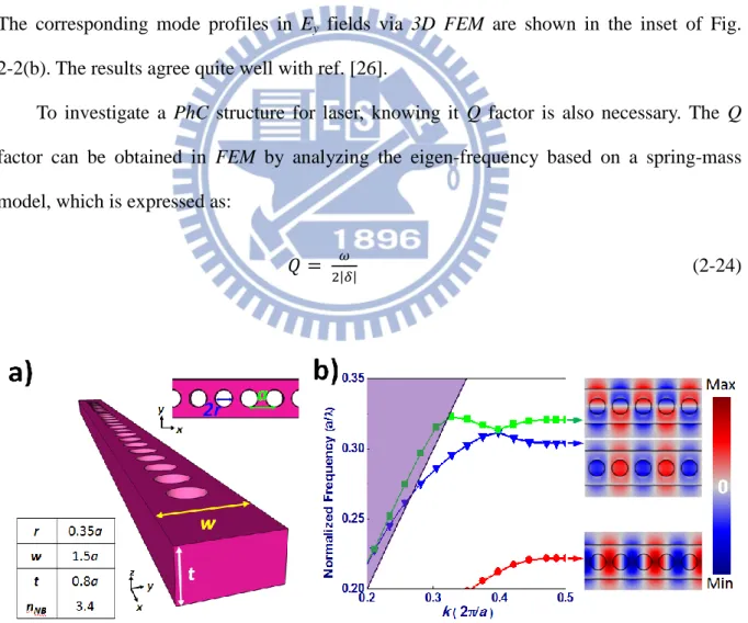
T o show the reliability of the simulation methods in section 2.2, we calculate the band diagram and modal properties of the dielectric band in a suspended nanobeam (NB) with one-dimensional (1D) PhCs. Scheme of 1D PhC NB is shown in Fig. 2-2(a), where 1D PhCs are composed of the air holes. Several important parameters are also defined in Fig. 2-2(a) including air hole radius r, lattice constant a, NB width w, NB thickness t, and NB index nNB.
With r/a, w, t, and nNB of 0.35, 1.5a, 0.8a, and 3.4, the same with those in ref. [26], the
corresponding band diagram obtained by 3D PWE method is shown in Fig. 2-2(b).The first three bands are the dielectric, air, and 1st-order dielectric bands from low to high frequencies. The corresponding mode profiles in Ey fields via 3D FEM are shown in the inset of Fig.
2-2(b). The results agree quite well with ref. [26].
To investigate a PhC structure for laser, knowing it Q factor is also necessary. The Q factor can be obtained in FEM by analyzing the eigen-frequency based on a spring-mass model, which is expressed as:
(2-24)
Fig. 2-2: (a) Scheme of 1D PhC NB and its (b) propagating band diagram via PWE method. (c) The mode profiles in Ey field of the first three bands at k = 0.5.
14
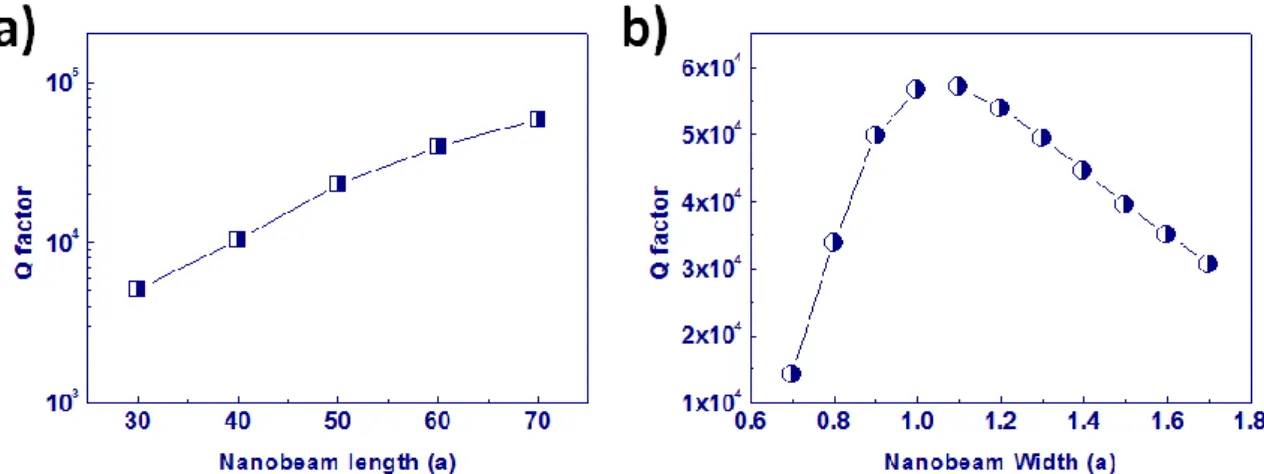
Fig. 2-3: Theoretical Q factor of the dielectric bandedge mode as a function of NB (a) length and (b) width via 3D FEM.
where the ω and δ are eigen-frequency and damping loss. Via this expression in FEM, we calculate the Q factor of dielectric band at kx = 0.5 in 1D PhC NB with parameters shown in
Fig. 2-2(a) and finite NB length varied from 30a to 70a. With fixed w of 1.5a, the theoretical
Q factor of the dielectric band at kx = 0.5 increases monotonically when PhC period number
increases, as shown in Fig. 2-3(a). In addition, an optimal Q value of 5.66×10⁴ can be obtained when w = 1a with NB length of 60a, as shown in Fig. 2-3(b). The results shown in Fig. 2-3(a) and(b) agree quite well with those obtained via finite-difference time-domain (FDTD) method in reference [26], which verify the accuracy of the FEM simulation for modeling PhC nano-structures.
2.3 Fabrication Process of PhC (III-V Materials) Nano-Structue on SiO
2Because of indirect electronic band gap of silicon (Si), integration of III-V active materials on Si-based substrate may be a feasible solution for light emission in Si photonics. To reach this goal, various bonding strategies have been demonstrated, including SiO2-SiO2
di rect bondi n g [ 33 ] , Au/ In eut e ct i c bo ndi ng [ 34] , spi n -on-gl ass [ 35 ] , and DVS-bis-Benzocyclobutene (BCB) bonding [36-39]. These bonding techniques can realize the
15
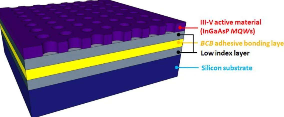
Fig. 2-4: Schematic of PhC structure on III-V active material (InGaAsP MQWs) with underlying low index SiO2 on Si substrate.
improve the thermal properties of PhC devices. In addition, the asymmetric PhC structures also provide stable and reliable mechanical property comparing to the suspended PhC slabs. In this thesis, BCB adhesive bonding is used to realize the asymmetric PhC structure shown in Fig. 2-4. Details of the fabrication processes will be illustrated in the following sections.
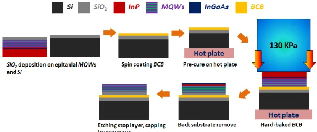
2.3.1
Transferring MQWs on SiO
2/Si Substrate via Adhesive Bonding
To transfer III-V active material onto SiO2 substrate, at first, InGaAsP MQWs and Si
wafers are prepared. The InGaAsP MQWs epitaxial structure with InGaAs etching stop layer shown in Fig. 2-5(a) is grown by Union Optronics Corp., Taiwan, which has total thickness ranging from 140 to 220 nm and photoluminescence peak near 1550 nm shown in Fig. 2-5(b). Then the MQWs and silicon wafer are both deposited by 800 nm SiO2 layer by plasma
enhanced chemical vapor deposition (PECVD, Oxford Instrument Plasma Technology Plasmalab 80 Plus) shown in Fig. 2-5(c) at 80oC.
To joint these t wo wafers, adhesive bonding technique via commercial DVS-bis-benzocyclobutene (BCB, Cyclotene-4022-35, Dow Chemical Company) is utilized. The steps are illustrated in details in the following and the flow chart is shown in Fig. 2-6.
16
Fig. 2-5: (a) Epitaxial structure of InGaAsP MQWs on InP substrate and (b) it PL spectrum with peak wavelength near 1540 nm. (c) Picture of PECVD, facilities of Center for Nano-Science Technology (CNST), National Chiao Tung University (NCTU).
1. The BCB solution is spin-coated on the SiO2/Si wafer as an adhesive layer and then
pre-cured at 60oC for 4 minutes to eliminate the bubbles inside
2. The InGaAsP MQWs and SiO2/Si wafers are clamped together and then hard-baked for
BCB polymerizing with uniform pressure of 130 KPa at 250oC for 2 hours.
3. After the hard-baking process, the InP substrate of the InGaAsP MQWs is removed via diluted HCl (HCl : H2O = 3 : 1) wet-etching at room temperature.
4. Then the InGaAs etching-stop and InP capping layers are removed via H3PO4 : H2O2 : H2O
= 1 : 1 : 8 and HCl solutions in sequence to leave MQWs on SiO2 substrate.
17
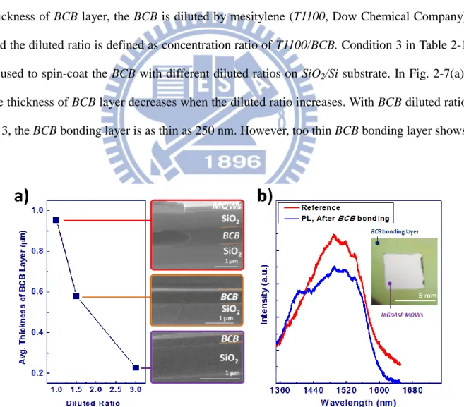
Table 2-1: Average thickness of the BCB layer under different spin-coating conditions. Condition Stage 1 Stage 2 Avg. BCB Layer Thickness
1 1000 r.p.m, 10 sec. 4500 r.p.m, 30 sec. 6.80 μm 2 3000 r.p.m, 30 sec. 6000 r.p.m, 60 sec. 4.41 μm
3 6000 r.p.m, 120 sec. 6000 r.p.m, 120 sec. 3.54 μm
In step 1, the adhesive strength and thickness of BCB bonding layer are decided by different spin-coater conditions and diluted ratios. To investigate the properties, at first, the non-diluted BCB is spin-coated with different conditions shown in Table 2-1. In Table 2-1, the thickness of BCB layer decreases when the spin speed increases. To further reduce the thickness of BCB layer, the BCB is diluted by mesitylene (T1100, Dow Chemical Company) and the diluted ratio is defined as concentration ratio of T1100/BCB. Condition 3 in Table 2-1 is used to spin-coat the BCB with different diluted ratios on SiO2/Si substrate. In Fig. 2-7(a),
the thickness of BCB layer decreases when the diluted ratio increases. With BCB diluted ratio of 3, the BCB bonding layer is as thin as 250 nm. However, too thin BCB bonding layer shows
Fig. 2-7: (a) Average thickness of the BCB layer under spin coating condition 3 and different diluted ratios shown in Table 2-1. The corresponding cross-section SEM pictures are also shown as the insets. (b) PL spectrum and picture (inset) of InGaAsP MQWs on SiO2/Si
18
weak adhesive strength between MQWs and SiO2. To provide sufficient bonding strength,
spin-coater condition 3 and diluted ratio of 1 are used, while the average bonding layer thickness is about 1 μm. The PL spectrum and smooth surface of InGaAsP MQWs on SiO2/Si
substrate after BCB bonding process are shown in Fig. 2-7(b).
2.3.2
Fabrication Processes of Asymmetric PhC Device
The MQWs on SiO2/Si substrate via BCB adhesive bonding is then followed by a series
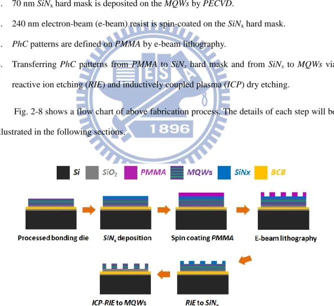
of fabrication process illustrated in the following to realize PhC nanostructures on it. 1. 70 nm SiNx hard mask is deposited on the MQWs by PECVD.
2. 240 nm electron-beam (e-beam) resist is spin-coated on the SiNx hard mask.
3. PhC patterns are defined on PMMA by e-beam lithography.
4. Transferring PhC patterns from PMMA to SiNx hard mask and from SiNx to MQWs via
reactive ion etching (RIE) and inductively coupled plasma (ICP) dry etching.
Fig. 2-8 shows a flow chart of above fabrication process. The details of each step will be illustrated in the following sections.
Fig. 2-8: The flow chart of realizing PhC structures on the MQWs on SiO2/Si substrate via
19
Fig. 2-9: The measured PL spectrum and picture (inset) of MQWs after depositing SiNx.
2.3.3.1 Depositing SiN
xHard Mask and Defining PhC Patterns
First, aSiNx hard mask with thickness of 70 nm is deposited on the MQWs by PECVD.
The deposition condition is shown in Table 2-2. The picture of MQWs after SiNx deposition
and the measured PL spectrum are shown in Fig. 2-9. It is worthy to note that the thickness of the SiNx hard mask is chosen as only sufficient for holding the following PhC pattern
transferring via ICP dry etching. After the ICP dry etching, the remaining thickness of the
SiNx hard mask would be less than 10 nm. Thus, the following RIE process for cleaning the
SiNx residue, which may etch the underlying SiO2, can be left out. And then we spin-coating
240 nm electron-beam (e-beam) resist (polymethyl methacrylate, PMMA) on the deposited
SiNx hard mask. The PhC patterns are defined on PMMA by e-beam lithography (EBL,
ELS–7500EX) system shown in Fig. 2-10(a). Finally, the defined PhC patterns on PMMA are developed by methyl-isobutyl ketone (MIBK) and fixed by iso-propyl (IPA) solution at 25oC. Fig. 2-10(b) shows the SEM picture of 2D PhCs on PMMA.
Table 2-2: SiNx hard mask deposition condition via PECVD. SiH4 [sccm] NH3 [sccm] N2 [sccm] T [oC] P [mTorr]
RF Power [W] Deposition Rate [nm/min]
20
Fig. 2-10: (a) EBL system (ELS - 7500EX), facilities of CNST, NCTU. (b) Top-view SEM picture of defined 2D PhCs on PMMA.
Fig. 2-11: (a) RIE-ICP system, facilities of CNST, NCTU. (b) SEM picture of transferred PhCs on SiNx hard mask. (c) The measured PL spectrum of MQWs after transferring the PhC
patterns into SiNx via RIE.
2.3.3.2 Transferring PhC Patterns via Dry Etching Process
To transfer the defined PhC patterns on PMMA into SiNx and MQWs, the reactive ion
etching/inductively coupled plasma (RIE/ICP, Oxford Instruments Plasma Technology Plasmalab 100) shown in Fig. 2-11(a) are used. For transferring PhC patterns from PMMA to
SiNx hard mask, CHF3/O2 mixed gas in RIE etching mode at 20oC is used. SEM picture of
transferred PhCs on SiNx hard mask is shown in Fig. 2-11(b). The measured PL spectrum of
MQWs after transferring PhC pattern into SiNx via RIE in Fig. 2-11(c) only slightly degrades
21
Then we use CH4/Cl2/H2 mixed gas to transfer the PhC patterns into MQWs in ICP
etching mode at 20 oC. Dry etching at low temperature can avoid the phase change of BCB bonding layer. The etching rate of InP/InGaAsP is about 412 nn/min and selectivity ratio to
SiNx is about 5. The recipe of RIE and ICP etching modes are listed in Table 2-3. The
measured PL spectrum of MQWs after ICP dry etching is shown in Fig. 2-12(a). Fig. 2-12(b) shows the top-view SEM picture of square-PhCs on InGaAsP MQWs on SiO2/Si substrate
after a series of dry etching steps. The zoom-in tilted-view SEM picture in the inset of Fig. 2-12 shows the etching profile and clearly observed underlying SiO2. Fig. 2-13 shows the
overview of fabrication processes of PhC light emitters based on InGaAsP MQWs on SiO2/Si
substrate.
Table 2-3: Recipe of RIE and ICP mode.
CHF3 [sccm] O2 [sccm] CH4 [sccm] Cl2 [sccm] H2 [sccm] T [oC] P [mTorr] RF Power [W] ICP Power [W] RIE Mode 50 5 - - - 20 55 150 - ICP Mode - - 4.5 8.5 3.5 20 4 100 1200
Fig. 2-12: (a) The measured PL spectrum of MQWs after transferring PhC pattern into MQWs via ICP dry etching. (b) Top- and tilted-view SEM pictures of a square-PhCs on SiO2/Si
22
Fig. 2-13: Flow chart of fabricating PhC nano-structures on MQWs on SiO2/Si substrate.
2.4 Measurement Setup
Fig. 2-14 shows the scheme of NIR confocal micro-PL system for characterizing the light emissions from PhC nano-structures. In this measurement s etup, an 845 nm transistor-transistor logical (TTL) laser (Power Technology Inc., APMT-60) with pulse or continuous-wave (CW) operations is used for pumping the devices. For the pulse operation, the output current from the DC power supply is modulated by a function generator (Stanford
Inc., DG-535). An attenuator and a depolarizer are put in front of the laser to control the
output power and maintain the un-polarization of the pump laser. The pump laser beam is split into two beams by a 50/50 beam splitter (Thorlabs, BP-150). One beam is focused on the sample with about 6 μm pump spot sizes in diameters on the PhC devices by 50x long working distance objective lens (NA = 0.42) (Mitsutoyo, M-plan 50x). The other beam is fed into a silicon power meter to estimate the power pump on the sample. The sample is mounted on a 3-axes piezo-stage used to adjust the alignments between the pumping spot and PhC devices. A microscopic system with co-axial white light source and a charge-coupled device (CCD) is used to monitor this adjustment. The light emission is collected by the 50x long
23
Fig. 2-14: Schematic of the NIR confocal micro-PL measurement system.
working distance objective lens and fed into a multimode fiber (MMF) via a 10x objective lens. To block the reflected pump light, a doubly-polished silicon wafer is put in front of the lens. Then the emission is analyzed by an optical spectrum analyzer (OSA) (Ando Inc., AQ-6315A) and a InGaAs power meter (Advantest Inc., Q8221).
2.5 Demonstration of Microdisk Laser on SiO
2/Si substrate
To simply confirm the laser emission can be obtained from the resonator based on the
MQWs on SiO2/Si substrate, we fabricate a microdisk with diameter of 3.56 μm on SiO2/Si
substrate, as shown in Fig. 2-15(a) and (b). In measurements, under optical pulse excitation with 6.7 mW peak powers, a single mode lasing at 1538.2 nm is observed, as shown in Fig. 2-15(c). The theoretical whispering-gallery (WG) mode profile in electric field with azimuthal number of 15 obtained from 3D FEM simulation is also shown as the inset in Fig. 2-15(c). This demonstration implies that we can demonstrate different kinds of nano-photonic light emitters based on this asymmetric structure.
24
Fig. 2-15: (a) Scheme of a microdisk on SiO2/Si substrate. (b) Top-view SEM picture and (c)
single mode lasing spectrum at 1538.2 nm of a microdisk with 3.56 μm in diameter on SiO2/Si
substrate. Theoretical lasing WG mode profile in electric field with azimuthal number of 15 via 3D FEM is shown as the inset of (c).
2.6 Summary
In this chapter, we have introduced the numerical methods, including PWE and FEM for modeling PhC nanostructures. The modal properties of the dielectric band in 1D PhC NB are also simulated to guarantee the accuracy of the methods. The BCB adhesive bonding techniques and nano-fabrication processes of PhCs are also introduced for realizing PhC active (InGaAsP MQWs) devices on SiO2/Si substrate. The NIR micro-PL system used to
characterize the optical properties of fabricated PhC devices is also introduced. To verify this asymmetric structure is feasible for active nanophotonic devices, single WG mode lasing emission from a microdisk with 3.56 μm in diameter on SiO2/Si substrate is demonstrate.
25
Chapter 3
Photonic Crystal Band-Edge Lasers
on SiO
2Substrate
3.1 Introduction
As we mentioned in chapter 1, photonic crystal (PhC) band-edge (BE) laser utilizes the flat photonic band with local group velocity vg ~ 0 near high symmetric points to enhance
light-matter interactions and achieves lasing operations. Owing to this mechanism, this kind of device shows less requirement of high Q design in achieving lasing. In addition, because the BE mode lasing occurs in the PhCs with large area and without delicate defect design, this type of device can be fabricated by high throughput fabrication processes with large fabrication tolerance. However, this feature also leads to a very large device footprint. In chapter 3.2, at first, we demonstrate and investigate the lasing properties of two-dimensional (2D) square-PhC BE laser on SiO2 substrate both in simulations and experiments for reference.
To further reduce device footprint of the 2D square-PhC, PhCs are eliminated in one dimension and lead to a 1D PhC nanobeam (NB) BE laser on SiO2 substrate. The modal
properties in simulation and lasing characteristics in experiments are shown and discussed in chapter 3.3.
3.2 Optical Properties of 2D Square-PhC BE Lasers on SiO
2Substrate
Scheme and top-view scanning electronic microscope (SEM) picture of 2D square PhC
BE laser on SiO2 substrate are shown in Fig. 3-1(a). To understand the BE mode in 2D
square-PhC on SiO2, at first, we calculate the transverse-electric (TE)-like photonic band
diagram of PhCs with air-hole radius (r) over lattice constant (a) (r/a) ratio of 0.22 and
InGaAsP multi-quantum-wells (MQWs) thickness t of 200 nm by three-dimensional (3D)
26
InGaAsP (nInGaAsP) are set as 1.44 and 3.4 respectively. In Fig. 3-1(b), we focus on the first
two bands from low to high frequencies below light-line (slab modes). Via 3D finite element method (FEM), the BE mode profiles in electric fields of the first and second bands at high symmetric X and M points, denoted as X0, X1, M0, and M1, are show in Fig. 3-1(c).
To evaluate which mode will be the lasing mode in our design, at first, the gain region of
InGaAsP MQWs (red shadow region in Fig. 3-1(b)) overlaps with the modes are considered.
In Fig. 3-1 (b), obviously, M0, and M1 BE modes coincide with the gain region. Second, from
the mode profiles in electric fields in Fig. 3-1(d), both M0 and M1 BE mode shows strong field
Fig. 3-1: (a) Scheme and top-view SEM pictures of 2D square-PhCs on SiO2 substrate. (b)
The photonic band diagram of 2D square-PhCs with r/a = 0.22 and t = 200 nm on SiO2
substrate via 3D PWE method. The gain region of InGaAsP MQWs is denoted by the red shadow. (c) Simulated electric field distribution of X0, X1, M0, and M1 BE modes by 3D FEM.
(d) Theoretical Q factors ofX0, X1, M0, and M1 BE modes in 2D square-PhC on SiO2 under
27
concentrates in the dielectric region, which means stronger light-matter interactions. In addition, quality (Q) factor is also the key property for deciding a mode lasing or not. Thus, the Q factors of X0, X1, M0, and M1 BE modes under different total period numbers are
calculated by 3D FEM and shown in Fig. 3-1(d). In Fig. 3-1(d), we can see the Q factor of M1
BE mode is always higher than the other three modes. Therefore, M1 BE mode should be the
lasing mode in the device. In our following fabrication, total period numbers of the devices are chosen to be 32, while the Q factor of M1 BE mode is ~ 7 × 10³.
Fig. 3-2: (a) Measured lasing spectrum in dB scale with lasing wavelength at 1578 nm and
SMSR of 30 dB from 2D square-PhC BE laser on SiO2. (b) L-L curve of 2D square-PhC BE
laser on SiO2 shows threshold power of 4.25 mW. The inset shows the lasing spectra under
different pump power. (c) Lasing spectra from 2D square-PhC on SiO2 under different r/a
ratios and the measured lasing frequencies and simulated M1 mode frequency under different
r/a ratio of 2D square-PhC BE laser on SiO2. (d) The measured polarization with polarized
28
Table 3-1: Duty cycle used in different structures.
Duty Cycle
PhC Lasers on SiO2 Substrate 1.5 – 2 %
2D PhC Lasers on Suspended Slab 0.75 %
1D PhC Lasers on Suspended NB 0.15 %
The devices are optically pumped via 845 nm diode laser with 15 ns pulse width. In the following measurements of PhC lasers on SiO2 in this thesis, 1.5 - 2 % duty cycle is used,
which are higher than the values that we usually used in suspended structures, as shown in Table 3-1. This is attributed to the underlying SiO2 with good thermal conductivity.
The measured single mode lasing spectrum at 1578 nm from a device with a = 460 nm and r/a ratio = 0.21 is shown in Fig. 3-2(a), which shows high side-mode suppuration ratio (SMSR) of 30 dB. And the measured light-in light-out (L-L) curve shows a threshold power of 4.25 mW. This milli-watt level threshold value is owing to the large pump area and the underlying lossy SiO2 layer. Lasing spectra under different pump power from 4.4 to 7.3 mW
are also shown as the inset of Fig. 3-2(b). Only single mode lasing is observed, which is the feature of BE laser.
To identify this lasing mode, the measured lasing spectra from 2D square-PhCs with different r/a ratios on SiO2 are shown in Fig. 3-2(c), where the lasing wavelength shows a red
shift when r/a decreases. In Fig. 3-2(c), the measured wavelengths match with simulated frequencies of M1 BE mode under different r/a ratios via 3D PWE simulation. The difference
between simulated results and measured results may come from the fabrication imperfection, thickness variation of MQWs, or value estimated from SEM picture. Therefore, we can conclude the lasing mode is the M1 BE mode. To further confirm this, polarization of the
lasing mode is also measured, as shown in Fig. 3-2(e). The low polarized ratio of 1.8 is because neither Ex nor Ey fields dominate in the M1 BE mode, as shown in the insets of Fig.
29
Although we demonstrate 2D square-PhC BE laser on SiO2 substrate via M1 BE mode.
High threshold of 4.25 mW is not only attributed to the lossy SiO2 substrate, but also owing to
the large device footprint of 14.8 × 14.8 μm2 caused by 2D square-PhCs. The definitions of device footprints of PhC lasers investigated in this thesis are given in Appendix A. To reduce the device footprint and threshold, eliminating PhCs in one-dimension to form 1D PhC NB investigated in the next section will be a feasible solution.
3.3 1D PhC NB BE Lasers on SiO
2Substrate
To further reduce the device footprint, we investigate a 1D PhC NB BE laser on SiO2
substrate, which is formed by periodic air holes on a ridge waveguide on SiO2 substrate, as
shown in Fig. 3-3(a). Actually, this structure can be regarded as eliminating PhCs in 2D square-PhCs in one dimension. The important parameters are defined in Fig. 3-3(a), including
NB thickness (t), NB width (w), air-hole radius (r), lattice constant (a), refractive index of NB
(nNB), and refractive index of SiO2 (nSiO2). With t = 200 nm, w = 1.4a, and r/a = 0.33, the
simulated band diagram of 1D PhC NB on SiO2 via 3D PWE method is shown in Fig. 3-3(b).
The first three bands from low to high frequencies are dielectric-, air-, and 1st-order dielectric
Fig. 3-3: (a) Scheme and important parameters of 1D PhC NB on SiO2 substrate. (b) Photonic
band diagram of 1D PhC NB on SiO2 substrate via 3D PWE. The mode profiles in Ey fields of
30
bands respectively. Their mode profiles in Ey fields at k = 0.5 via 3D FEM are shown as inset
of Fig. 3-3(b). According to their mode profiles, the dielectric band shows good overlaps with the gain medium, which is beneficial for active laser. Therefore, in the following researches, we will focus on the dielectric mode only.
3.3.1
Modal Properties of Dielectric Band in Simulations
At first, we calculate the wavelength, Q, and V of the dielectric mode in 1D PhC NB on
SiO2 as a function of total PhC period numbers (P), as shown in Fig. 3-4(a) and (b). The
effective mode volume V is expressed as:
(3-1)
The parameters of t, a, r/a, and w of 1D PhC NB are 200 nm, 400 nm, 0.35, and 1.2a respectively. The simulated wavelength in Fig. 3-4(a) shows a blue shift when P increases and then saturates when P > 30. In addition, in Fig. 3-4(b), both Q and V increase with P. In 1D
PhC BE laser, without the photonic band gap (PBG) confinement one of the main optical
losses comes from the finite PhCs along the NB. When P increases, this loss is significantly reduced. And this results in the increase of Q. Moreover, because the BE mode is an extended mode, it is reasonably that the V increases with P.
Fig. 3-4: Theoretical (a) wavelength, (b) Q, and V of the dielectric mode as a function of P in
31
Fig. 3-5: Theoretical Q and V as a function of (a) beam width w (with fixed r/a = 0.35) and (b)
r/a ratio (with fixed w = 1.3a), while t, a, and P are fixed at 200 nm, 400nm, and 28
respectively.
We then further investigate the influence of different beam width w and r/a ratio on Q and V individually. At first, with fixed t, a, r/a, and P of 200 nm, 400 nm, 0.35, and 28, there is an optimized Q value of ~ 3,070 when w = 1.3a, as shown in Fig. 3-5(a).Two mechanisms are responsible for this optimization. First, when w is smaller than 1.3a, more fields in the NB penetrate into the air region, thus decreases the Q values. Second, when w becomes larger than 1.3a, the photonic band becomes steep and the group velocity at kx = 0.5 will increase.
Increased group velocity means reduced slow light effect and leads to decreased Q. In addition, V decreases because the mode field concentrates more inside the NB.
Moreover, with fixed t, a, w, and P of 200 nm, 400 nm, 1.3a, and 28, theoretical Q and V under different r/a ratios are shown in Fig. 3-5(b). An optimal Q ~ 3,100 can be obtained when r/a = 0.36. There are also two mechanisms responsible for this optimal value. The first one is that the group velocity at kx = 0.5 becomes higher when r/a ratio decreases, which leads
to the decreased Q. The other one is that the effective index of NB decreases when r/a ratio increases, which leads to weakened TIR effect responsible for the decreased Q. And the theoretical V is about 1.2 (λ/nInGaAsP)3 when r/a = 0.36, which is attributed to the extended
![Fig. 1-5: SEM pictures and mode profiles of 1D PhC NB nanocavities with (a) parabolic beam width modulation [23] and (b) effective index matching [24]](https://thumb-ap.123doks.com/thumbv2/9libinfo/8378930.178089/18.892.132.805.434.1055/pictures-profiles-nanocavities-parabolic-width-modulation-effective-matching.webp)