國
立
交
通
大
學
電子物理學系
碩
士
論
文
在共平面磁場中與 Rashba 及 Dresselhaus 自旋
軌道交互作用之窄通道的量子傳輸
Quantum transport of narrow-channels in in-plane magnetic
fields with Rashba and Dresselhaus spin-orbit interactions
研 究 生:張書瑜
指導教授:鄭舜仁 教授
在共平面磁場中與 Rashba 及 Dresselhaus 自旋 軌道交
互作用之窄通道的量子傳輸
Quantum transport of narrow-channels in in-plane magnetic
fields with Rashba and Dresselhaus spin-orbit interactions
研 究 生:張書瑜 Student:Shu-Yu Chang
指導教授:鄭舜仁 教授 Advisor:Prof. Shun-Jen Chen
國 立 交 通 大 學
電 子 物 理 學 系
碩 士 論 文
A Thesis
Submitted to Department of Electrophysics College of Science
National Chiao Tung University in partial Fulfillment of the Requirements
for the Degree of Master
in
Electrophysics
Nov. 2010
Hsinchu, Taiwan, Republic of China
在共平面磁場與 Rashba 及 Dresselhaus 自旋軌道交互作用之
窄通道的量子傳輸
學生:張書瑜 指導教授:鄭舜仁 教授
國立交通大學電子物理研究所碩士班
摘要
我們研究考慮共平面磁場與 Rashba 及 Dresselhaus 自旋軌道交互作用之窄通 道的同調量子傳輸。因為 Rashba 及 Dresselhaus 自旋軌道交互作用造成能帶水平 方向的仳裂,而外加共平面磁場則造成能帶垂直方向的仳裂。首先,當我們同時 考慮 Rashba 自旋軌道交互作用及共平面磁場時,能帶中,會出現虛能隙。在調 變磁場大小的過程中,我們觀察電子自旋方向的改變。傳輸特性上,我們發現了 似電子和似電洞的準束縛態。而當我們同時考慮共平面磁場與 Rashba 及 Dresselhaus 自旋軌道交互作用時,能帶開始變得不對稱。在傳輸特性上,除了發 現似電子和似電洞的準束縛態之外,我們發現了 Fano 效應。因此,在考慮 Rashba 自旋軌道交互作用及共平面磁場時,Dresselhaus 效應對傳輸特性有重大的影響。Quantum transport of narrow-channels in in-plane magnetic
fields with Rashba and Dresselhaus spin-orbit interactions
Student:Shu-Yu Chang Advisor:Shun-Jen Cheng
Department of Electrophysics
National Chiao Tung University
ABSTRACT
We investigate coherent electronic quantum transport in a narrow channel with Rashba and Dresselhaus spin-orbit interaction in the presence of an external in-plane magnetic field that is applied along the channel direction. The spin-split energy spectrum is horizontally shifted respectively by the Rashba and the Dresselhaus effects and is vertically shifted by the applied magnetic field. First, we consider the Rashba spin-orbit interaction and the in-plane magnetic field in the narrow channel, there is a pseudo-gap in the energy spectrum. With the increasing magnetic field, we investigate the variation of the spin orientation. Furthermore, we find the hole-like quasi bound state and electron-like quasi-bound state features in conductance. When we consider the Rashba, Dresselhaus and Zeeman effects simultaneously, energy spectrum becomes asymmetry. In some specific cases, except for the quasi-bound state feature, we find the Fano effect in transport properties. Hence, in the presence of the Rashba spin-orbit interaction and the in-plane magnetic field, the Dresselhaus effect significantly affects coherent magneto-quantum transport properties.
致謝
很開心可以從交大畢業了,兩年的碩士生活過的很充實。特別感謝
唐志雄老師,總是擁有許多的耐心,不厭其煩的和我解釋相同的物理觀
念。在每個禮拜五的討論時間,總是讓我獲益良多。老師也很願意和我
們打成一片,分享生活中的許多樂趣。感謝鄭舜仁老師的細心指導,從
老師身上學習到做事情以及處理事情的嚴謹態度,這將讓我往後的人生
道路上受用無窮。也感謝口試委員,朱仲夏老師以及關肇正老師給的寶
貴意見,使我了解到自己的研究還有哪些細節需要注意。
碩班生活中,有時快樂、也有時低落,很感謝有以理、毓謙的陪伴。
謝謝你們在我忙碌的時候,陪我ㄧ起在研究室待到很晚。在我口試前,
陪我ㄧ起奔波,甚至在口試當天,都比我還緊張了。很開心能夠認識你
們,在兩年的研究生活中,彼此互相扶持著,很令人感到溫暖。感謝我
的家人的默默陪伴,因為知道你們是無比的支持我,使我的內心能夠更
強大,無後顧之憂的專注在課業研究上,謝謝你們,真的很愛你們。感
謝博文、俊弦、志榮,很關心我也很鼓勵我,使我能夠更勇敢的面對生
活中的挑戰。感謝可愛的安頡,每個禮拜四看到你,聽你的童言童語,
是我最放鬆快樂的時候。以及可愛的 Happy,雖然你看不懂我的論文,
但我還是很愛你很謝謝你的陪伴,晚上在實驗室做研究時,你都會乖乖
的趴在旁邊陪我。
最後,感謝實驗室的夥伴們,以及陳煜璋老師的學生們,很開心能
夠認識你們,讓我的碩班生活更增添色彩,謝謝你們的相伴。
Contents
Abstract in Chinese
ii
Abstract in English
iii
1 Introduction to charge transport in semiconductors 1
1.1 Introduction to semiconductors………1
1.2 Low dimensional semiconductor systems………1
1.2.1 Introduction to heterostructure semiconductors…………...1
1.2.2 Modeling the low dimensional semiconductor systems……..3
1.3 Quantum transport in quasi-one-dimensional quantum systems...4
1.3.1 Introduction to quantum transport………...4
1.3.2 Quasi-one-dimensional quantum systems………...5
1.3.3 Analytical approach……….6
1.3.4 Numerical approach……….8
2 Spin-resolved quantum transport 9
2.1 Introduction to spintronics………9
2.2 The spin-orbit interactions and the Zeeman effect……….10
3 Quantum transport in the presence of the Rashba spin-orbit
interaction with in-plane magnetic field 12
3.1 Theory……….12
3.1.1 System and Formulation………..12
3.1.2 The Rashba effect………18
3.1.3 The Zeeman effect………...20
3.1.4 Spin orientation………...21
3.2 Transport theory………..25
3.3 Numerical results………29
3.3.1 Ideal conductance with the tunable Rashba effects……...29
3.3.2 Transport properties with the Rashba effects in the
presence of in-plane magnetic field………..31
4 Quantum transport in the presence of Rashba and Dresselhaus
spin-orbit interactions with in-plane magnetic field 35
4.1 Theory………...35
4.1.1 System and Formulation………..35
4.1.2 The Dresselhaus effects………...38
4.1.3 The Rashba and Dresselhaus effects………42
4.1.4 The Zeeman effects………..44
4.1.5 Complex energy dispersion……….48
4.2 Spin-resolved transport theory………..49
4.3 Numerical results………..52
4.3.1 Ideal conductance with tunable the Dresselhaus effects…52
4.3.2 Ideal conductance with the tunable Rashba and
Dresselhaus effects……….54
4.3.3 The Dresselhaus effects in the presence of the Rashba
spin-orbit interaction and in-plane magnetic field……..56
4.3.4 Transport properties with the Rashba-Dresselhaus effects
in the presence of an in-plane magnetic field………….60
5 Conclusion and future work 65
Bibliography 66
List of Figures
1.2.1.1. The bandage profile of semiconductor heterostructures…………2
1.2.1.2. The conduction-band edge across a graded AlGaAs-GaAs
heterojunction in thermal equilibrium………..3
1.2.2.1. The GaAs/AlGaAs high electron mobility transistor………4
1.3.2.1. System figuration………...5
1.3.3.1. System picture………...6
1.3.4.1. Conductance (in units of 2e
2/h) versus kinetic energy in a
quantum channel with tunable potential strength V
0………8
3.1.1.1. System picture……….…13
3.1.1.2. (a) For the case 2α
2> gB, energy spectrum with labeling local
energy extreme values and corresponding wavevectors. (b) For
the case 2α
2≤ g
B
, energy spectrum with labeling local energy
extreme values and corresponding wavevectors………15
3.1.1.3. For the case of considering the Rashba effect and turning off the
magnetic field B = 0, energy spectrum with labeling local energy
extreme values and corresponding wavevectors………16
3.1.1.4. For the case of considering only the in-plane magnetic field and
the Rashba coefficient
α
= 0, energy spectrum with labeling
local energy extreme values and corresponding wavevectors....17
3.1.2.1. Energy spectrum versus wave number with magnetic field
strength gB = 0.02 for different values of α: (a) α = 0.0 (b) α =
0.05, (c) α = 0.1, and (d) α = 0.2 (the Rashba-Zeeman effect).
The Fermi energy E
F= 66 meV and the Fermi wave vector
k
F= 2×10
6cm
-1. The magnetic field strength is approximately 3T
when gB = 0.02 (g
s= −15 for InAs). The black and red curves
indicate the plus (σ = +) and minus (σ =
−) spin branches,
respectively. The black dot and the red dot correspond to the
local minima of plus and minus branches at the subband bottoms,
denoted by P
b+and P
b-. The red circle stands for the local
maxima of the minus branch at the subband top,
denoted by P
t-…………...……18
3.1.3.1 Energy spectrum versus wave number with different magnetic
field strength gB and the fixed Rashba strength α: (a) gB = 0, α =
0.2; (b) gB = 0.04, α = 0.2; (c) gB = 0.08, α = 0.2 (d) gB = 0.12, α
= 0.2. The Fermi energy E
F= 66 meV and the Fermi wave vector
k
F= 2×10
6cm
-1. The magnetic field strength is approximately 6T
when gB = 0.04 (g
s= −15 for InAs). The black and red curves
indicate the plus (σ = +) and minus (σ =
−) spin branches,
respectively. The black dot and the red dot correspond to the local
minima of plus and minus branches at the subband bottoms,
denoted by P
b+and P
b-. The red circle stands for the local
maxima of the minus branch at the subband top,
denoted by P
t-………..….20
3.1.4.1. Energy dispersion with spin orientation illustrated by the arrows
with the different Zeeman effects and the fixed Rashba strength α.
(d) gB = 0.12, α = 0.2. The magnetic field strength is
approximately 6T when gB = 0.04 (g
s= −15 for InAs)…………22
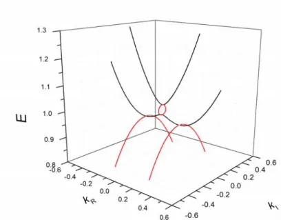
3.1.5.1. 3D Energy dispersion in the presence of the Rashba spin-orbit
interaction and in-plane magnetic field (α = 0.2, gB = 0.02). k
Rand k
Irepresent, respectively, the real part and the imaginary part
of the wave number (k = k
R+ k
I). The black solid line represents
the propagating modes and the red solid line represents the
evanescent modes. The Fermi energy E
F= 66 meV and the
Fermi wave vector k
F= 2×10
6cm
-1………24
3.2.1. Energy spectrum with labeling modes. k
1, q
1indicate the outer
right-going and left-going modes. k
2, q
2in this energy regime are
evanescent modes………..….26
3.2.2. Scattering process in the high energy regime………...………...28
3.3.1.1. Conductance (in units of G
0= e
2/h) versus kinetic energy without
the scattering potential in the presence of in-plane magnetic field
with different Rashba coefficients: (a)
α
= 0, gB = 0.02; (b)
α
=
0.05, gB = 0.02; (c)
α
= 0.1, gB = 0.02; (d)
α
= 0.2, gB = 0.02.
The Fermi energy E
F= 66 meV and the Fermi wave vector k
F= 2
×10
6cm
-1. The magnetic field strength is approximately 3T when
gB = 0.02 (g
s= −15 for InAs)……….29
3.3.2.1. Conductance (in units of G
0= e
2/h) versus kinetic energy with the
attractive scattering potential in the presence of in-plane magnetic
field with different Rashba coefficients: (a) α = 0.0, gB = 0.02
(2α
2< gB) (b) α = 0.05, gB = 0.02 (2α
2< gB) (c) α = 0.1, gB =
0.02 (2α
2= gB) (d) α = 0.2, gB = 0.02 (2α
2> gB). The Fermi
energy E
F= 66 meV and the Fermi wave vector k
F= 2×10
6cm
-1.
The magnetic field strength is approximately 3T when gB = 0.02
(g
s= −15 for InAs)………31
3.3.2.2. Conductance (in units of G
0= e
2/h) versus kinetic energy with the
repulsive scattering potential in the presence of in-plane magnetic
field with different Rashba coefficients: (a) α = 0.0, gB = 0.02
(2α
2< gB) (b) α = 0.05, gB = 0.02 (2α
2< gB) (c) α = 0.1, gB =
0.02 (2α
2= gB) (d) α = 0.2, gB = 0.02 (2α
2> gB). The Fermi
energy E
F= 66 meV and the Fermi wave vector k
F= 2×10
6
cm
-1.
The magnetic field strength is approximately 3T when gB = 0.02
(g
s= −15 for InAs)………33
4.1.1.1. System picture……….36
4.1.2.1. Energy spectrum versus wave number in the presence of the
Rashba spin-orbit interaction and in-plane magnetic field with
different Dresselhaus coefficients: (a) α = 0.2, β = 0.0, gB = 0.02
(b) α = 0.2, β = 0.1, gB = 0.02 (c) α = 0.2, β = 0.2, gB = 0.02 (d) α
= 0.2, β = 0.3, gB = 0.02. The Fermi energy E
F= 66 meV and the
Fermi eave vector k
F= 2×10
6cm
-1. The magnetic field strength is
approximately 3T when gB = 0.02 (g
s= −15 for InAs). The black
and red curves indicate the plus (σ = +) and minus (σ = −) spin
branches, respectively. The black dot and the red dot correspond
to the local minima of plus and minus branches at the subband
bottoms, denoted by P
b+and P
b-. The red circle stands for the
denoted byP
t-………..38
4.1.2.2. Energy spectrum versus wave number in the presence of the
Rashba, the Dresselhaus and the Zeeman effects with different
Dresselhaus strength. (a) α = 0.2, β = 0.0, gB = 0.0 (b) α = 0.2, β
= 0.1, gB = 0.0 (c) α = 0.2, β = 0.2, gB = 0.0 (a) α = 0.2, β = 0.3,
gB = 0.0. The Fermi energy E
F= 66 meV and the Fermi eave
vector k
F= 2×10
6cm
-1. The black and red curves indicate the
plus (σ = +) and minus (σ = −) spin branches,
respectively………...40
4.1.3.1. Energy spectrum versus wave number in the presence of in-plane
magnetic field with different Rashba and Dresselhaus
coefficients. (a) α = β = 0.01, gB = 0.02 (b) α = β = gB = 0.02 (c)
α = β = 0.1, gB = 0.02 (d) α = β = 0.2, gB = 0.02. The Fermi
energy E
F= 66 meV and the Fermi eave vector k
F= 2×10
6
cm
-1.
The magnetic field strength is approximately 3T when gB = 0.02
(g
s= −15 for InAs). The black and red curves indicate the plus (σ
= +) and minus (σ = −) spin branches, respectively. The black
dot and the red dot correspond to the local minima of plus and
minus branches at the subband bottoms, denoted by P
b+and P
b-.
The red circle stands for the local maxima of the minus branch at
the subband top, denoted by P
t-………..…………...42
4.1.4.1. Energy spectrum versus wave number in the presence of the
Rashba, the Dresselhaus and the Zeeman effects with different
Dresselhaus strength. (a) α = β = 0.2, gB = 0.0 (b) α = β = 0.2,
gB = 0.1 (c) α = β = 0.2, gB = 0.2 (d) α = β = 0.2, gB = 0.3. The
Fermi energy E
F= 66 meV and the Fermi eave vector k
F= 2×10
6
cm
-1. The magnetic field strength is approximately 15T when gB
= 0.1 (g
s= −15 for InAs). The black and red curves indicate the
plus (σ = +) and minus (σ = −) spin branches, respectively. The
black dot and the red dot correspond to the local minima of plus
and minus branches at the subband bottoms, denoted by P
b+and
P
b-……….………..44
4.1.4.2. Energy dispersion with spin orientation illustrated by the arrows
in the presence of the fixed Rashba and Dresselhaus spin-orbit
interactions with different Zeeman coefficients. (a) α = β = 0.2,
gB = 0.0 (b) α = β = 0.2, gB = 0.1 (c) α = β = 0.2, gB = 0.2 (d)
α = β = 0.2, gB = 0.3. The magnetic field strength is
approximately 15T when gB = 0.1 (g
s= −15 for InAs)…...46
4.1.5.1. 3D Energy dispersion in the presence of the spin-orbit
interactions and in-plane magnetic field (α = β = 0.2, gB = 0.02).
k
Rand k
Irepresent, respectively, the real part and the imaginary
part of the wave number (k = k
R+ k
I). The black solid line
represents the propagating modes and the red solid line
represents the evanescent modes.
The Fermi energy E
F= 66 meV
and the Fermi eave vector k
F= 2×10
6cm
-1……….48
4.2.1. The scattering process in the high energy regime…….………..51
4.3.1.1. Conductance (in units of G
0= e
2/h) versus kinetic energy without
the scattering potential in the presence of the Rashba spin-orbit
interaction and in-plane magnetic field with different
Dresselhaus coefficients: (a)
α
= 0.2, β = 0.0, gB = 0.02; (b)
α
=
0, β = 0.1, gB = 0.02; (c)
α
= 0.2, β = 0.2, gB = 0.02; (d)
α
= 0, β
= 0.3, gB = 0.02. The Fermi energy E
F= 66 meV. The magnetic
field strength is approximately 3T when gB = 0.02 (g
s= −15 for
InAs)……....52
4.3.2.1. Conductance (in units of G
0= e
2/h) versus kinetic energy without
the scattering potential in the presence of in-plane magnetic field
with different Rashba and Dresselhaus coefficients: (a) α = β =
0.01, gB = 0.02 (b) α = β = gB = 0.02 (c) α = β = 0.1, gB = 0.02
(d) α = β = 0.2, gB = 0.02. The Fermi energy E
F= 66 meV. The
magnetic field strength is approximately 3T when gB = 0.02 (g
s= −15 for InAs)………...……54
4.3.3.1. Conductance (in units of G
0= e
2
/h) versus kinetic energy with the
attractive scattering potential in the presence of the Rashba
spin-orbit interaction and in-plane magnetic field with different
Dresselhaus coefficients: (a) α = 0.2, β = 0.0, gB = 0.02 (b) α =
0.2, β = 0.1, gB = 0.02 (c) α = 0.2, β = 0.2, gB = 0.02 (d) α = 0.2,
β = 0.3, gB = 0.02. The Fermi energy E
F= 66 meV. The
magnetic field strength is approximately 3T when gB = 0.02 (g
s= −15 for InAs)………..….56
4.3.3.2. Scattering process in the presence of the true bound state……..57
4.3.3.3. Conductance (in units of G
0= e
2/h) versus kinetic energy with the
repulsive scattering potential in the presence of the Rashba
spin-orbit interaction and in-plane magnetic field with different
Dresselhaus coefficients: (a) α = 0.2, β = 0.0, gB = 0.02 (b) α =
0.2, β = 0.1, gB = 0.02 (c) α = 0.2, β = 0.2, gB = 0.02 (d) α = 0.2,
β = 0.3, gB = 0.02. The Fermi energy E
F= 66 meV. The magnetic
field strength is approximately 3T when gB = 0.02 (g
s= −15 for
InAs)……….59
4.3.4.1. Conductance (in units of G
0= e
2/h) versus kinetic energy with the
attractive scattering potential in the presence of in-plane
magnetic field with different Rashba and Dresselhaus
coefficients: (a) α = β = 0.01, gB = 0.02 (b) α = β = gB = 0.02 (c)
α = β = 0.1, gB = 0.02 (d) α = β = 0.2, gB = 0.02. The Fermi
energy E
F= 66 meV. The magnetic field strength is
approximately 3T when gB = 0.02 (g
s= −15 for InAs)………..60
4.3.4.2. Scattering process in the presence of the true bound state……..61
4.3.4.3. Scattering process in the presence of the true bound state……..62
4.3.4.4. Conductance (in units of G
0= e
2
/h) versus kinetic energy with the
repulsive scattering potential in the presence of in-plane magnetic field
with different Rashba and Dresselhaus coefficients: (a) α = β = 0.01, gB =
0.02 (b) α = β = gB = 0.02 (c) α = β = 0.1, gB = 0.02 (d) α = β = 0.2, gB =
0.02. The Fermi energy E
F= 66 meV. The magnetic field strength is
Chapter 1 Introduction to charge transport in semiconductors
1.1 Introduction to semiconductors
The term “semiconductor” represents a certain class of solid materials. It suggests that the electrical conductivity is intermediate in magnitude between a conductor and an insulator. Semiconductor materials are numerous and versatile. We can distinguish it into elementary semiconductors and compound semiconductors.
Elementary semiconductors are Silicon (Si) and germanium (Ge), phosphorous (P), sulfur (S), selenium (Se), and tellurium (Te). Compound semiconductors are categorized following by the group of their constituents in the periodic table of elements. Such as gallium arsenide (GaAs), aluminium arsenide (AlAs), indium arsenide (InAs), indium antimonide (InSb), gallium antimonide (GaSb), gallium phosphide (GaP), gallium nitride (GaN), aluminium antimonide (AlSb), and indium phosphide (InP) are all belong to the so-called III-V semiconductors. There are also II-VI semiconductors, such as zinc sulfide (ZnS), zinc selenide (ZnSe) and cadmium telluride (CdTe), III-VI compounds, such as gallium sulfide (GaS) and indium selenide (InSe), as well as IV-VI compounds, such as lead sulfide (PbS), lead telluride (PbTe), lead selenide (PbSe), germanium telluride (GeTe), tin selenide (SnSe), and tin telluride (SnTe).
For compound semiconductors, there are two chemical constituents are called binary compounds. Additionally, there are compound semiconductors with three constituents, such as AlxGa1−xAs (aluminium gallium arsenide), InxGa1−xAs (indium gallium arsenide), and also InxGa1−xP (indium gallium phosphide). In this situation, it is called about ternary semiconductors or semiconductor alloys.
( , , ) x y z
H x y z =H +H +H (1.1.1)
1.2 Low dimensional semiconductor systems
1.2.1 Introduction to heterostructure semiconductors
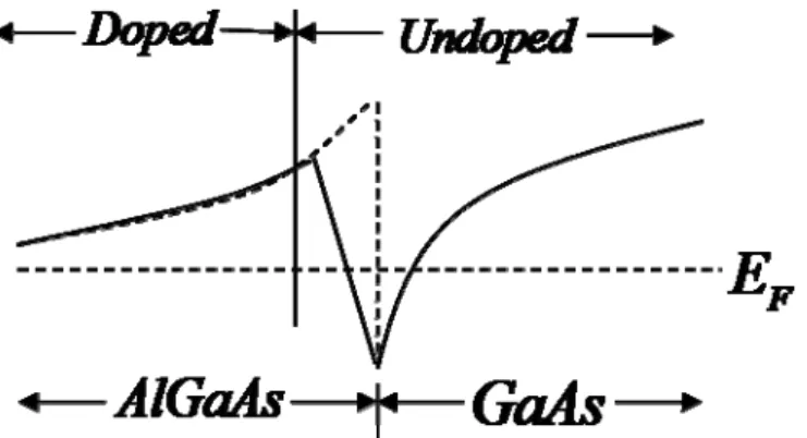
For heterostructure, since the two different materials will have two different energy bandgaps, the energy band will have a discontinuity at the junction interface. We may have an abrupt junction in which the semiconductor changes abruptly from a narrow bandgap material to a wide-band gap material. In Fig. 1.2.1.1 shows the energy-band diagram of a GaAs-AlGaAs heterojunction in thermal equilibrium. The
AlGaAs is moderately to heavily doped n type, while the GaAs is more lightly doped or even intrinsic. In order to achieve thermal equilibrium, electrons flow from the wide-bandgap AlGaAs into the GaAs, forming an accumulation layer of electrons in the potential well adjacent to the interface. The electrons contained in a potential well are quantized. The two-dimensional electron gas refers to the condition in which the electrons have quantized energy levels in one spatial direction (perpendicular to the interface), but are free to move in the other two spatial directions.
Fig. 1.2.1.1. The bandage profile of semiconductor heterostructures.
Since the GaAs is lightly doped or intrinsic, the two-dimensional electron gas is in a region of low impurity doping so that impurity scattering effects are minimized. The electron mobility will be much larger than if the electrons were in the same region with the ionized donors. The movement of the electrons parallel to the interface will still be influenced by the coulomb attraction of the ionized impurities in the AlGaAs. The effect of these forces can be further reduced by using a graded AlGaAs-GaAs heterojunction. The graded layer is AlxGa1-xAs in which the fraction x varies with distance. In this situation, an intrinsic layer of graded AlGaAs can be sandwiched between the N-type AlGaAs and the intrinsic GaAs. Fig. 1.2.1.2 shows the conduction-band edge across a graded AlGaAs-GaAs heterojunction in thermal equilibrium. The electrons in the potential well are further separated from the ionized impurities so that the electron mobility is increased above that in an abrupt heterojunction.
Fig. 1.2.1.2. the conduction-band edge across a graded AlGaAs-GaAs heterojunction in thermal equilibrium.
The two-dimensional electron gas (2DEG) trapped at a doped heterostructure is the most important low-dimensional system for electronic transport. It forms the kernel of a field-effect transistor. The high electron mobility transistor has many acronyms including modulation-doped field-effect transistor (MODFET) and high electron mobility transistor (HEMT).
1.2.2 Modeling the low dimensional semiconductor systems
Fig. 1.2.2.1 is the GaAs/AlGaAs high electron mobility transistor. The cap layer in the transistor can prevent the n-type AlGaAs from oxidizing. Above the cap layer, we use two metal gates to define a quasi-one dimensional quantum channel. The Hamiltonian of a semiconductor with heterostructure can be written separately in the vertical and lateral parts of form
( , , ) z H x y z =H +H , (1.2.2.1) where
(
)
2 2 2 * ( , ) 2 x y H k k V x y m = + + (1.2.2.2) and 2 2 * ( ) 2 z z c k H V z m = + . (1.2.2.3)Vc(z) is the quantum well at the interface of the heterostructure. The electrons underneath the gate oxide are confined to the heterostructure interface, and thus occupy well defined energy levels. Nearly always, only the lowest level is occupied, and so the motion of the electrons perpendicular to the interface can be ignored. While, the electron can be free to move in the other two spatial directions. Hence, we can ignore the z-part Hamiltonian and emphasize the x, y dependant Hamiltonian (Eq. 1.2.2.2).
Fig. 1.2.2.1. The GaAs/AlGaAs high electron mobility transistor.
1.3 Quantum transport in quasi-one-dimensional quantum systems
1.3.1 Introduction to quantum transport
In macroscopic systems, the conductance obeys an ohmic scaling law: W
G L σ
= . (1.3.1.1)
As the dimensions become smaller, there are two corrections to this law. Firstly there is an interface resistance independent of the length L of the sample. Secondly the conductance does not decrease linearly with the width W anymore. Instead it depends on the number of transverse modes in the quantum channel. The Landauer-Buttiker formula incorporates both of these features [1, 2]:
2
2e
G NT
h
= . (1.3.1.2)
The factor T is the average probability that an electron incident from the source will transmit to the drain, the factor 2 is for the spin and N is the number of propagating modes with positive group velocity due to transverse confinement. The Landauer-Buttiker formalism only applies to coherent transport. In this paper, we assume that the phase-coherent length is larger than the sample of linear size L, in which lφ > and the elastic mean free path is larger than the sample size L le> . L Namely, our system is in the coherent quantum transport regime.
1.3.2 Quasi-one-dimensional quantum systems
To form a quasi-one-dimensional quantum system (Fig. 1.2.2.1), we use two split top gates above the HEMT. We can rewrite the Eq. 1.2.2.2 in the following form:
(
)
2 2 2 * ( , ) ( ) ( , ) 2 x y c s H x y k k V y V x y m = + + + . (1.3.2.1)Since the two split top gates are quite near each another, electrons will be confined in the quantum channel and can only propagate along the x direction. Hence, the single particle Hamiltonian in the narrow channel can be described by.
2 2 * ( , ) 2 k H V x y m = + . (1.3.2.2)
This Hamiltonian can be separated into two parts:
2 2 * ( ) 2 y y c k H V y m = + . (1.3.2.3) 2 2 * ( ) 2 x x k H V x m = + (1.3.2.4)
VC(y) indicates the confining potential in the transverse direction. The corresponding eigenvalue of Hy is the sub-band energy. In the narrow channel, the electron
propagates along x direction whose kinetic energy will be the total energy of an incident electron subtracting the subband energy Ek = Etot - εn, εn depends on which
subband the electron occupying. V(x) exhibits the x dependant potential which can be the spin orbit interaction or the scattering potential in longitudinal direction. In this chapter, we consider the system is only with the static scattering potential along x direction without spin orbit interaction. In the following chapters, we will discuss the spin-resolved transport properties including both the static scattering potential and spin orbit interaction.
1.3.3 Analytical approach
The system figuration is shown in Fig. 1.3.2.1. A static finger gate is in the middle of the narrow channel. The system under investigation can be described by the Hamiltonian: 2 0 * ( ) ( ) 2 c p H V y V x m δ = + + , ( ) 1 2 2 2 c y V y = mω y (1.3.3.1)
In order to simplify the calculation, the dimensionless Hamiltonian is introduced by choosing appropriate physical units: the length unit * 1
F l k = , the energy unit * 2 2 2 * F k E m
= , and the unit of the parameter ωy of the confining potential
*
* 2
y
E ω = . Following performing standard dimensionless the Hamiltonian becomes:
2 2 2 0 ( ) y H =k +ω y +Vδ x . (1.3.3.2) x y z split gate split gate 1 x x Ga Al As−
GaAs
2DEG B x y z split gate split gate 1 x x Ga Al As−GaAs
2DEG B x y z x y z split gate split gate 1 x x Ga Al As−GaAs
2DEG BFig. 1.3.3.1. System picture.
The wave function can factorize into functions of x and y, as follows:
( )
ψ( ) ( )x ϕ yΨ r = . (1.3.3.3)
Since the confining potential in the transverse direction is a parabolic potential, the wavefunction and the subband energy will be
(2 1) n n y ε = + ω . (1.3.3.4) and
( )
2 2 0 2 0 0 1 2 ! x x n n n x x e H x n x ψ π − ⎛ ⎞ = ⎜ ⎟ ⎝ ⎠. (1.3.3.5)The electrons incident from the left source will be scattered by the static delta potential in the middle of the quantum channel. The electrons may be back scattered or forward scattered. Therefore, the x-part wave functions can be written in the form:
0, ( ) ikx ikx x< ψ x =e +re− (1.3.3.6) and 0, ( ) ikx, n x> ψ x =te k= E−ε . (1.3.3.7) r, t represent the reflected and transmitted coefficients. E is the total energy of the electron and εn is the subband energy. The wavefunctions should satisfy these
boundary conditions:
(i) (ψ x=0 )− =ψ(x=0 )+ (1.3.3.8)
and
(ii)ψ′(x=0 )− =ψ′(x=0 )+ −V0ψ(x=0 )+ . (1.3.3.9)
Substituting the x-part wave functions into these boundary conditions can obtain:
1 r t= − (1.3.3.10) and 0 (1 ) ik − =r ikt V t− . (1.3.3.11)
Combining these two equations and using linear algebra, the transmitted coefficient can be expressed as:
0 1 1 2 t V ik = − . (1.3.3.12) Once obtaining the transmitted coefficient, we can substitute it into the Landauer-Büttiker equation and acquire the conductance.
2 2 2 2 0 2 2 2 1 | | 1 4 n n n e e G t V h h k = = +
∑
∑
. (1.3.3.13)1.3.4 Numerical approach
In this section, we show the numerical results and discussion of the variation of conductance with the potential strength V0. The numerical calculations presented
below are carried out under the assumption that the electron effective mass m* = 0.067m0, which is appropriate to the GaAs-based semiconductors. The typical
electron density is n ~ 1011 cm-2. Accordingly, the energy unit E* = 9 meV , the length unit L* = 7.96 nm, and the frequency unit ω*= E* =13.6 THz[3].
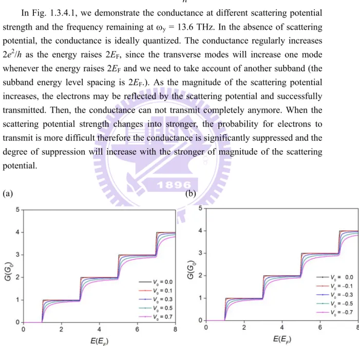
In Fig. 1.3.4.1, we demonstrate the conductance at different scattering potential strength and the frequency remaining at ωy = 13.6 THz. In the absence of scattering
potential, the conductance is ideally quantized. The conductance regularly increases 2e2/h as the energy raises 2EF, since the transverse modes will increase one mode
whenever the energy raises 2EF and we need to take account of another subband (the
subband energy level spacing is 2EF.). As the magnitude of the scattering potential
increases, the electrons may be reflected by the scattering potential and successfully transmitted. Then, the conductance can not transmit completely anymore. When the scattering potential strength changes into stronger, the probability for electrons to transmit is more difficult therefore the conductance is significantly suppressed and the degree of suppression will increase with the stronger of magnitude of the scattering potential.
(a) (b)
Fig. 1.3.4.1. Conductance (in units of 2e2/h) versus kinetic energy in a quantum channel with tunable potential strength V0 (a) The potential is repulsive (b) The potential is attractive. The
Chapter 2 Spin-resolved quantum transport
2.1 Introduction to spintronics
In the recent years, there has been growing interest in the emerging field of spin electronics or “spintronics”. Spintronics, where the spin of electrons is used to carry information, is a rapidly growing area of research [4−6]. There are several techniques for generating pure spin currents [7–9]; Spintronics involves exploration of the extra degrees of freedom provided by the electron spin, in addition to those due to electron charge, with a new view to realize the new functionalities in future electronic devices.
Spin-orbit interaction (SOI) is considered as an efficient manipulation via gate voltages, which is a relativistic effect that couples the electron spin, momentum, and electric field (or momentum dependant effective magnetic field in the electron frame.) The SOI has been utilized to devise various spintronics devices such as spin transistors, spin logic, and spin filters [10−13].
In 1990, Datta and Das proposed to control the strength of Rashba spin-orbit interaction using gate voltage as a spin-field transistor based on spin rotation, which can be a significant strong effect in narrow gap semiconductor heterostructures [14]. The gate control of the spin current employing the Aronov-Casher effect was considered. The electric dipole spin resonance controlled by the time-dependant gate was also studied. Furthermore, spin-orbit interaction is likely to be important in Einstein-Podolsky-Rosen type spin-dependant entangled electronic states for quantum information processing [15, 16]. Considering semiconductor systems, there are two main types of spin-orbit interaction. The Dresselhaus spin-orbit interaction [17] appears due to the asymmetry present in certain crystal lattices.
The Rashba spin-orbit interaction [18] arises due to the asymmetry associated with the confining potential of the heterostructure quantum well. The perpendicular electric fields inside heterostructure quantum wells are important for understanding spin-orbit coupling, which is sample-specific and adjustable. In narrow gap semiconducting quantum wells, a variation of about 50% of the spin-orbit coupling coefficient was observed experimentally by adjusting the voltage on adjacent gate electrodes, in which a quantum well is populated only by donor-layer electrons. Consequently, much interest has been attracted to the realization of spin polarized transistors, spin filter devices, and other devices based on electrical gate control to the spin-dependant transport.
2.2 The spin-orbit interactions and the Zeeman effect
To realize a spin device, it is important to utilize the spin-orbit interaction since it provides a way of controlling the spin degree of freedom electrically in semiconductor-based systems. Moreover, for a quasi-one-dimensional ballistic it is found that the SOI could significantly modify the band structure, thus additional subband extrema and energy gaps are produced. Effects of SOI and Zeeman splitting on the physical properties of quantum wires, e.g., photovoltaic effect [19] and shot noise [20] have been investigated in detail. Li et al [21]. have presented that the SOI and the Zeeman effect could result in significant variations of the conductance and the thermopower which are spin-dependent.
We will consider the transport properties in the presence of the SOI and the in-plane magnetic field. The spin-orbit interaction can be caused by structural inversion asymmetry (SIA), which can be artificially controlled by the applied gate voltages or by the specific design of the heterostructure, or by bulk inversion asymmetry (BIA), which is determined by the semiconductor material and the geometry of the sample. Both HBIA and HSIA lead to spin splitting of the conduction
band linear in k. The in-plane magnetic field will cause the energy splitting that is independent of k.
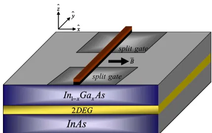
The structural inversion asymmetry results in the Rashba spin-orbit interaction. The Rashba spin-orbit interaction depends on the gradient of the potential and is therefore more important the higher the nuclear charge of the element. In Ch. 1.2.1, we have mentioned that the electrons are confined at the heterostructure interface. For the purpose of confining electrons to nanostructure devices, potential well is necessary. The potential well at the interface results in the non-negligible Rashba spin–orbit interaction (SOI), especially in systems with structural inversion asymmetry (SIA) like e.g. semiconductor heterostructures. Heavy elements in the periodic table show stronger effects. This is also valid in crystals. For instance, in silicon the spin-orbit interaction is much weaker than in Ge or GaAs. It is even more important in InAs and InSb. In a two-dimensional electron gas (2DEG) obtained by a strong confinement in the z-direction (Fig. 1.3.3.1), the Rashba SOI is described by the Rashba term
(
)
R y x x y z
H =α pσ −pσ . (2.2.1)
The components of the electron momentum operator are denoted by pi, the Pauli
matrices are represented by σi, and α proportional to Ez is the SOI coupling coefficient
In III-V or II-VI the heterostructure semiconductors, such as, the difference between cations and anions breaks the degeneracy of the band structure with respect to the spin degree of freedom, and is present in both bulk materials and semiconductor nanostructures. The electric fields resulting from the lack of an inversion centre lead to bulk inversion asymmetry (BIA) and to the Dresselhaus term in the Hamiltonian. In the conduction band, the spin splitting Hamiltonian is given by
(
2 2)
(
2 2)
(
2 2)
,
bulk D c x x y z y y z x z z x y
H =γ σ⎣⎡ k k −k +σ k k −k +σ k k −k ⎤⎦ . (2.2.2) To obtain the effective Hamiltonian of the two-dimensional quantum channel, we take the average of the above bulk Hamiltonian with respect to the ground state wave function along the vertical z direction.
(
)
D x x y y
H = β pσ −p σ . (2.2.3)
The components of the electron momentum operator are denoted by pi, the Pauli
matrices are represented by σi, and β is the Dresselhaus spin-orbit interaction strength.
An external magnetic field lifts time inversion symmetry so that we can obtain a finite Zeeman energy splitting ΔEZ = g∗μBB, where g∗ is the effective g factor and μB
the Bohr magneton of the electron or hole states. It was first shown by Roth et al. [22] that electrons can have an effective g factor g∗ that differs substantially from the
free-electron value g0 = 2. The effective g factor g∗ ≠ 2 results from the spin–orbit
interaction, which couples the orbital motion with the spin degree of freedom. Because of without SOI, the motion of spin-up electrons would be completely decoupled from the motion of spin-down electrons, and there would be identical Hamiltonians for spin-up and spin-down electrons except for the trivial Zeeman term ±(g0/2)μBB, so that in this case Zeeman splitting would be controlled by the g factor,
in which g0 = 2 of free electrons. Recently, calculations and experiments have shown
that g∗ can have different values for B applied in the direction normal to the plane of
the 2D system and for B in the plane of the quantum wire [23−26].
In Ch3 and Ch4, we will analyze the transport properties in a quantum channel in the presence of the spin-orbit interactions and in-plane magnetic field.
Chapter 3 Quantum transport in the presence of the Rashba
spin-orbit interaction with in-plane magnetic field
In this chapter, we will use the analytical approach to investigate how the Rashba spin-orbit interaction and an in-plane magnetic field affect the electron transport. We will introduce the system Hamiltonian and analyze the energy spectrum and the wavefunction in the first section. In the second section we will use the Landauer-Buttiker formula by the matching method to calculate the conductance. At last, we will demonstrate the numerical results under different strengths of the Rashba spin-orbit interaction, the magnetic field and the gate voltage.
3.1 Theory
In this section, we use the numerical approach to calculate the energy spectrum and the spinor states of the system considering both the Rashba and the Dresselhaus spin-orbit coupling and an in-plane magnetic field.
3.1.1 System and Formulation
In this paragraph, we use the analytical approach to derive the energy spectrum and the spinor states of the system considering the Rashba spin-orbit coupling and an in-plane magnetic field [27].
We use a transverse hard wall potential to simulate the confinement potential along y direction. The transverse potential is a narrow constriction therefore we can neglect the momentum py along y direction. Then, the Rashba term can be reduced
from Eq.(2.2.1) to
R x y
H = −α σp . (3.1.1.1)
The Hamiltonian for the quantum channel in the presence of the Rashba spin-orbit interaction and the Zeeman effect which is due to an applied magnetic field along x direction has the form
2 0 * 1 ( ) 2 x y 2 s B x c p H p g B V y m α σ μ σ = − + + , (3.1.1.2)
where α is the Rashba strength, B is the magnetic field strength and Vc is the confining
potential. In the middle of the quantum channel there is a scattering potential in forms of delta potential. Then the total single particle Hamiltonian is
0 s( )
x y z split gate split gate 1 x x In Ga As−
InAs
2DEG B x y z split gate split gate 1 x x In Ga As−InAs
2DEG B x y z x y z split gate split gate 1 x x In Ga As−InAs
2DEG BFig. 3.1.1.1. System picture
For convenience, we choose the following units: length unit * 1
F l k ≡ , energy unit 2 2 * * 2 F k E m
≡ , magnetic field unit
* * B E B μ
≡ , the Rashba coefficient unit
2 * * F k m α = , the
confinement potential in units of Fermi energy
( )
( )
*c
V y =V y E and defining
1 2 s
g≡ g . In the following way, we can obtain the dimensionless unperturbed Hamiltonian:
2
0 2 x y x ( )
H =k − α σk +gBσ +V y . (3.1.1.4) Separating the unperturbed Hamiltonian into the x-dependant and y-dependant parts can get: 0 0 0 x y H =H +H (3.1.1.5) with 0 2 2 x x x y x H =k − α σk +gBσ (3.1.1.6) and 0 2 ( ) y y H =k +V y , (3.1.1.7) where 0, ( ) 2 , otherwise d y V y ⎧ < ⎪ = ⎨ ⎪∞ ⎩ (3.1.1.8)
is a potential that confines the electron in the transverse direction and we suppose that the confining potential with only the lowest occupied subband.
The wavefunction of the unperturbed Hamiltonian can be expanded by the spatial wavefunction and spinor state,
( , ) ( ) ik xx
n
x y φ y e χ
Ψ = . (3.1.1.9)
Since the transverse confinement potential is the hard wall potential, the transverse wavefunction will be
( )
sin n n y y d d π π φ = ⎛⎜ ⎞⎟ ⎝ ⎠, (3.1.1.10)and the subband energy will be
2 n n d π ε = ⎜⎛ ⎞⎟ ⎝ ⎠ . (3.1.1.11)
Here, we only consider the lowest occupied subband. That is n is equal to 1. Then, substituting the transverse wavefunction and the subband energy into Eq. (3.1.1.4) and Eq. (3.1.1.9) obtain
2
( 2− α σkx y+gBσ χx) =(E− −εn kx )χ. (3.1.1.12) Expanding the above equation by the Pauli matrices:
2 0 2 ( ) 2 0 x n x x gB i k E k gB i k α χ ε χ α + ⎛ ⎞ = − − ⎜ − ⎟ ⎝ ⎠ . (3.1.1.13)
The spinor state and the eigen-energy can be obtained by solving the above eigenvalue problem. The spinor state is
( )
1
1
; =
2
e
i kx σ θχ
σ
σ
⎡
⎤
=
⎢
⎥
±
⎣
⎦
, (3.1.1.14) where 1 2 ( ) tank kx gB α θ ≡ − ⎛ ⎞ ⎜ ⎟ ⎜ ⎟ ⎝ ⎠, (3.1.1.15)and the energy is
2 2 2
( ) (2 )
n n x x
E± =ε +k +σ gB + αk , (3.1.1.16) where kx can only be real and σ = ± indicating the spin branches for a given subband n.
For an ideal wire without scattering potential, it is convenient to use Eq. (3.1.1.16) to obtain energy spectrum as a function of wave vector for propagating modes, as shown
in Secs. 3.1.2 and 3.1.3.
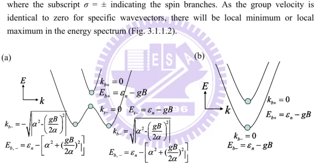
In general, there are four extreme values in the energy dispersion. For convenience, we define Pbσ = (kbσ, Ebσ) and Ptσ = (ktσ, Etσ) to denote the extreme
values of the energy dispersion at the subband bottom (b) and subband top (t), respectively. We also define ΔEZ to represent the pseudo-gap or the branch level
spacing for a given subband, respectively. In addition, σ = +, - represents the upper branch and lower branch, respectively.
To analyze the energy spectrum and find the local minimum and local maximum in the energy dispersion for the case involving both the Rashba and the Zeeman effects, it is convenient to define the group velocity, given by
2 n x x 2 2 2 2 x x 4 2 4 g dE k k dk g B k σ α υ σ α = = + + , (3.1.1.17)
where the subscript σ = ± indicating the spin branches. As the group velocity is identical to zero for specific wavevectors, there will be local minimum or local maximum in the energy spectrum (Fig. 3.1.1.2).
(a) 0 b k+ = b n E+ =ε −gB 0 t k− = Et−=εn−gB 2 2 -2 b gB k α α − ⎛ ⎞ = − ⎜ ⎟ ⎝ ⎠ 2 2 , (2 ) b n gB E ε α α − = −⎡⎢ + ⎤⎥ ⎣ ⎦ 2 2 -2 b gB k α α − ⎛ ⎞ = ⎜ ⎟ ⎝ ⎠ 2 2 , ( ) 2 b n gB E ε α α −= −⎡⎢ + ⎤⎥ ⎣ ⎦ E k 0 b k+ = b n E+ =ε −gB 0 t k− = Et−=εn−gB 2 2 -2 b gB k α α − ⎛ ⎞ = − ⎜ ⎟ ⎝ ⎠ 2 2 , (2 ) b n gB E ε α α − = −⎡⎢ + ⎤⎥ ⎣ ⎦ 2 2 -2 b gB k α α − ⎛ ⎞ = ⎜ ⎟ ⎝ ⎠ 2 2 , ( ) 2 b n gB E ε α α −= −⎡⎢ + ⎤⎥ ⎣ ⎦ E k E k (b) b n Ek−b−==ε0−gB 0 b k+ = b n E+ =ε −gB
E
k
b n Ek−b−==ε0−gB 0 b k+ = b n E+ =ε −gB b n Ek−b−==ε0−gB 0 b k+ = b n E+ =ε −gBE
k
E
k
Fig. 3.1.1.2. (a) For the case 2α2 > gB, energy spectrum with labeling local energy extreme values and corresponding wavevectors. (b) For the case 2α2 ≤ gB, energy spectrum with labeling local energy extreme values and corresponding wavevectors.
These local extreme values occur at
( , ) (0, ) t t t n P−= k E− − = ε −gB , (3.1.1.18) ( , ) (0, ) b b b n P+ = k + E + = ε +gB , (3.1.1.19) and 2 2 2 2 , ( , ) ( - , ( ) ) 2 2 b b b b n gB gB P k t α E ε α α α − − − − ⎛ ⎞ ⎡ ⎤ = = ± ⎜ ⎟ = −⎢ + ⎥ ⎝ ⎠ ⎣ ⎦ . (3.1.1.20)
It is noteworthy that this extreme value (Eq. 3.1.1.20) only exists as 2α2 > gB otherwise the value in the square root will be negative. Namely, this extreme value only occurs when the Rashba is significantly stronger than the Zeeman effects (Fig. 3.1.1.2 (a)). The gap between the upper branch and the lower branch would be
Z 2
E gB
Δ = . (3.1.1.21)
If the Rashba coefficient is not strong enough, the energy spectrum will be vertical splitting (Fig. 3.1.1.2(b)). The energy spacing between the upper branch and the lower branch is
Z 2
E gB
Δ = . (3.1.1.22)
For the specific cases, we consider only the Rashba effect, and then the energy dispersion (Eq. 3.1.1.16) becomes
2 2 n n x x E±=ε +k +σ αk . (3.1.1.23) b
k
+= −
α
k
b−= +
α
2 b nE
+=
ε α
−
2 b nE
−=
ε α
−
E
k
bk
+= −
α
k
b−= +
α
2 b nE
+=
ε α
−
2 b nE
−=
ε α
−
bk
+= −
α
k
b−= +
α
2 b nE
+=
ε α
−
2 b nE
−=
ε α
−
E
k
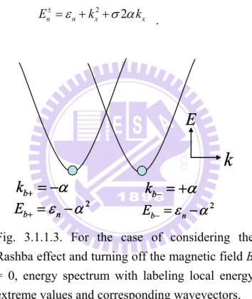
Fig. 3.1.1.3. For the case of considering the Rashba effect and turning off the magnetic field B = 0, energy spectrum with labeling local energy extreme values and corresponding wavevectors.
The energy dispersion is lateral splitting. The local extreme values which can be solved from the group velocity (Eq. 3.1.1.17) are at
2 ( , ) ( , ) b b b n P+ = k + E+ = −α ε α− , (3.1.1.24) and 2 ( , ) ( , ) b b b n P− = k − E− = α ε α− . (3.1.1.25)
If we consider only the Zeeman effect, the energy dispersion (Eq. 3.1.16) becomes 2 n n x E± =ε +k +σgB . (3.1.1.26) b n
E
k
−b−=
=
ε
0
−
gB
0
bk
+=
b nE
+=
ε
−
gB
E
k
b nE
k
−b−=
=
ε
0
−
gB
0
bk
+=
b nE
+=
ε
−
gB
b nE
k
−b−=
=
ε
0
−
gB
0
bk
+=
b nE
+=
ε
−
gB
E
k
E
k
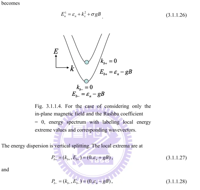
Fig. 3.1.1.4. For the case of considering only the in-plane magnetic field and the Rashba coefficient = 0, energy spectrum with labeling local energy extreme values and corresponding wavevectors.
The energy dispersion is vertical splitting. The local extrema are at
( , ) (0, ) b b b n P+ = k + E + = ε +gB , (3.1.1.27) and ( , ) (0, ) b b b n P− = k E− − = ε −gB , (3.1.1.28) which can be solved from the group velocity (Eq. 3.1.1.17). Then, the energy spacing between the upper branch and the lower branch is
2
Z
E gB
3.1.2 The Rashba effect
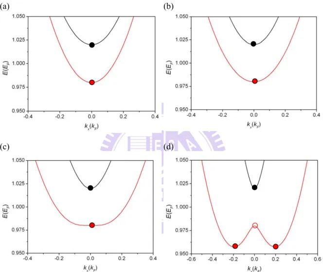
In this section, we investigate the energy spectrum with the different Rashba effect in the presence of the in-plane magnetic field (gB = 0.02). There are four cases: α = 0.0(2α2 < gB), 0.05(2α2 < gB), 0.1(2α2 = gB), and 0.2(2α2 > gB), as shown in Fig. 3.1.2.1. The magnetic field strength is approximately 3T when gB = 0.02 (gs = −15 for
InAs)
(a) (b)
(c) (d)
Fig. 3.1.2.1. Energy spectrum versus wave number with magnetic field strength gB = 0.02 for different values of α: (a) α = 0.0 (b) α = 0.05, (c) α = 0.1, and (d) α = 0.2 (the Rashba-Zeeman effect). The Fermi energy EF = 66 meV and the Fermi wave vector kF = 2×
106 cm-1. The magnetic field strength is approximately 3T when gB = 0.02 (gs = −15 for
InAs). The black and red curves indicate the plus (σ = +) and minus (σ = −) spin branches, respectively. The black dot and the red dot correspond to the local minima of plus and minus branches at the subband bottoms, denoted by Pb+ and Pb-. The red circle stands for the local
maxima of the minus branch at the subband top, denoted by Pt-.
In Fig. 3.1.2.1(a), we consider only the Zeeman effect. In the presence of the in-plane magnetic field, the energy spectrum is vertical splitting. The local minima are
at Pb− = (kb−, Eb−) = (0.0, εn − gB) = (0.0, 0.98), Pb+ = (kb+, Eb+) = (0.0, εn + gB) = (0.0,
1.02) and the branch level spacing for a given subband is ΔEZ = 2gB = 0.04 as we
mentioned in (Eq. 3.1.28). In the second case, the Rashba effect is week and not strong enough to form a pseudo-gap, that is, 2α2 < gB, therefore the energy spectrum is vertical splitting (Fig. 3.1.2.1(b)) and the local minima are Pb+ = (kb+, Eb+) = (0.0,
εn + gB) = (0.0, 1.02) and Pb− = (kb−, Eb−) = (0.0, εn − gB) = (0.0, 0.98). The branch
level spacing for a given subband is still ΔEZ = 2gB = 0.04. When the Rashba effect
satisfy 2α2 = gB, the energy spectrum is still vertical splitting and the local minima are the same as the first two cases. When the Rashba effect is strong enough to from a pseudo-gap, that is, 2α2 > gB, there isa magneto-spin-orbit pseudo-gap in the energy spectrum (Fig. 3.1.2.1(d)). The local minimum at the upper branch is Pb+ = (kb+, Eb+)
= (0.0, εn + gB) = (0.0, 1.02) (Eq. 3.1.19) and the local extreme values at the lower
branch are Pt− = (kt−, Et−) = (0.0, εn − gB) = (0.0, 0.98), Pb−,1 = (k b−,1 , E b−,1) = (0.1952,
0.9575) and Pb−,2 = (k b−,2 , E b−,2) = (0.1952, 0.9575) (Eq. 3.1.18 and 3.1.20). The
3.1.3 The Zeeman effect
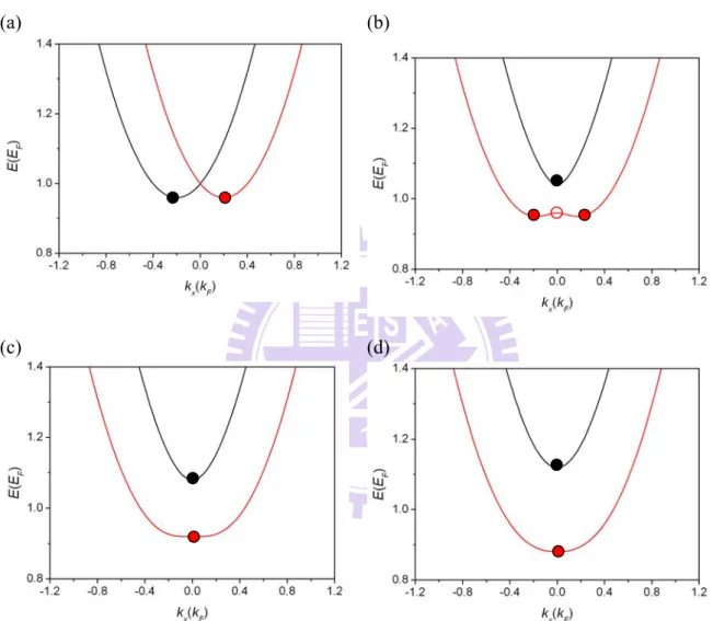
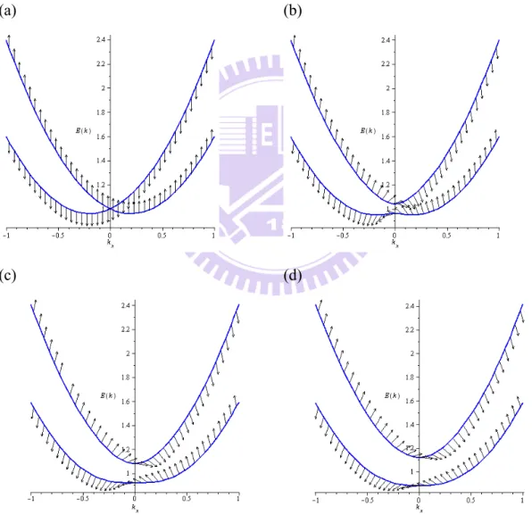
For comprehending how the Zeeman effect would affect the energy spectrum, we fix the Rashba effect (α = 0.2) and tune the Zeeman effect from weak to strong. Below, there are five cases: gB = 0(2α2 > gB), gB = 0.02(2α2 > gB), gB = 0.08 (2α2 = gB), gB = 0.1 (2α2 < gB).
(a) (b)
(c) (d)
Fig. 3.1.3.1 Energy spectrum versus wave number with different magnetic field strength gB and the fixed Rashba strength α: (a) gB = 0, α = 0.2; (b) gB = 0.04, α = 0.2; (c) gB = 0.08, α = 0.2 (d) gB = 0.12, α = 0.2. The Fermi energy EF = 66 meV and the Fermi wave vector kF = 2×
106 cm-1. The magnetic field strength is approximately 6T when gB = 0.04 (g
s = −15 for
InAs). The black and red curves indicate the plus (σ = +) and minus (σ = −) spin branches, respectively. The black dot and the red dot correspond to the local minima of plus and minus branches at the subband bottoms, denoted by Pb+ and Pb-. The red circle stands for the local
maxima of the minus branch at the subband top, denoted by Pt-.
spin-orbit interaction. The energy dispersion is lateral splitting. The local minimum at the plus branch is Pb+ = (kb+, Eb+) = (−0.2, 0.96) and at the minus branch is Pb- = (kb-,
Eb-) = (0.2, 0.96) (Eq. 3.1.24 and 3.1.25). In Fig. 3.1.3.1(b), when the Zeeman effect
gB = 0.04 and 2α2 > gB, there is a pseudo-gap in the energy spectrum. The local extreme value at the upper branch is Pb+ = (kb+, Eb+) = (0.0, 1.04). The local extreme
values at the lower branch are Pb- = (kb-,1, Eb-,1) = (−0.17, 0.95), Pb-,2 = (kb-,2, Eb-,2) =
(0.17, 0.95) and Pt,− = (kt,−, Et, −) = (0.0, 1.04) (Eq. 3.1.18 and 3.1.20). As the magnetic
field increases and gB = 0.08 and 2α2 = gB, the energy dispersion is vertical splitting (Fig. 3.1.3.1(c)) and the branch level spacing for a given subband is ΔEZ = 2gB = 0.16.
As the Zeeman coefficient increases (gB = 0.12) and satisfies 2α2 < gB, the branch level spacing compare to Fig. 3.1.3.1(c) increases ΔEZ = 2gB = 0.24 since the in-plane
magnetic field increases. 3.1.4 Spin orientation
In order to investigate the spin orientation in the presence of the Rashba spin-orbit interaction and the in-plane magnetic field, we calculate the effective magnetic field for these spin-orbit interactions and the Zeeman effect [28]. The dimensionless Hamiltonian for an electron in the presence of the magnetic field can be expressed as:
H = ⋅σ B, (3.1.4.1)
where B is dimensionless (B* = E*/μB). Hence, when the above equation is identical to
the Rashba term,
2α σkx y σ B Byσy
− = ⋅ = , (3.1.4.2)
we can obtain the effective magnetic field for the Rashba spin-orbit interaction: 2
R x
B = − αk y. (3.1.4.3)
In the same way, we can obtain the effective magnetic field for the Zeeman effect:
Z
B =gBx. (3.1.4.4)
Then, the effective magnetic field of the system can be expressed as: 2
eff Z R x
B =B x B y gBx+ = − αk y. (3.1.4.5) In order to achieve equilibrium, the spin orientation of the electron in the presence of the magnetic field tends to be opposite to the direction of the magnetic field. Therefore, the spin orientation of the electron at the plus branch is aligned in the direction of the effective magnetic field. However, the spin orientation of the electron
at the minus branch will be opposite to the direction of the effective magnetic field. We can express the spin orientation for the electrons at the plus branch as:
( ) (
2)
2( ) (
2)
2 2 2 2 x x x gB k S x y gB k gB k σ α α α = − + + , σ = + . (3.1.4.6)and the spin orientation for the electrons at the minus branch is:
( ) (
2)
2( ) (
2)
2 2 2 2 x x x gB k S x y gB k gB k σ α α α = − + + + , σ = −. (3.1.4.7)Below, we show the energy spectrum with the spin orientation in the presence of the Rashba spin-orbit interaction with different Zeeman effects.
(a) (b)
(c) (d)
Fig. 3.1.4.1. Energy dispersion with spin orientation illustrated by the arrows with the different Zeeman effects and the fixed Rashba strength α. (a) gB = 0, α = 0.2; (b) gB = 0.04, α = 0.2; (c) gB = 0.08, α = 0.2 (d) gB = 0.12, α = 0.2. The magnetic field strength is approximately 6T when gB = 0.04 (gs = −15 for InAs)