IEEE TRANSACTIONS ON MAGNETICS, VOL. 43, NO. 2, FEBRUARY 2007 939
Effect of Oxygen Concentration on Characteristics of
NiO
x
-Based Resistance Random Access Memory
Ming-Daou Lee
1, Chia-Hua Ho
2, Chi-Kuen Lo
3, Tai-Yen Peng
1, and Yeong-Der Yao
4Department of Materials Science and Engineering, National Chiao Tung University, Hsinchu 300, Taiwan, R.O.C. Nano-techology R&D Department/Emerging Central Laboratory, Macronix International Company, Ltd.,
Hsinchu 300, Taiwan, R.O.C.
Electronics Research & Service Organization, Industrial Technology Research Institute (ITRI), Hsinchu 310, Taiwan, R.O.C. Department of Materials Engineering, Tatung University, Taipei 104, Taiwan, R.O.C.
The resistance bistability and the switching effect has been systematically studied in nickel oxide films with variable oxygen concen-trations. Both the switching bias voltage and the resistance ratio of RESET to SET were found to be strongly concentration dependent. Meanwhile, the electrical characteristics can be exactly examined by an Schottky emission. By means of mathematical fitting, the resis-tance bistability seems to be related to the alternating of dielectric constant and the barrier height. Furthermore, the room temperature cycle endurance with a distinguishable operation window was found to exceed 800. This indicates that the nickel oxide has the potential to be a promising material on resistance random access memory.
Index Terms—NiO, resistance random access memory (RRAM), Schottky emission.
I. INTRODUCTION
T
HE data storage and transferring has become an important life processing during the recent decade. The processing is heavily reliant on the development of high-performance memory devices, especially for the non-volatile memory (NVM). The NAND-type Flash memory is widely used and attractively studied right now. Other novel memories, such as magnetic random access memory (MRAM), phase change random access memory (PCRAM), and resistance random access memory (RRAM), are also developed hard in order to potentially take the place of Flash memory or the embedded memory for special applications.The resistance bistability of RRAM has been reported in metal–insulator–metal (MIM) structure with Nb O [1], TiO [2], ZrO [3], Ta O [4], Al O [5], NiO [6], Cr-doped SrZrO , [7], (Pr,Ca)MnO [8], and Fe oxides ([9] and ref-erences therein). Much works has been done in this field, starting already during the late 1960s. Recently, NiO has been studied to be a promising industrial material due to its high resistivity ratio and simple constituents [10]. However, the physical mechanism of resistance bistability is still not clear yet due to the complicity of the noncrystalline semiconductor or insulator. In this study, a polycrystalline NiO films was found by a reactive ion beam deposition method. And we also report the electrical characteristics change of polycrystalline NiO films with variable oxygen concentrations. By means of
Digital Object Identifier 10.1109/TMAG.2006.888525
Color versions of one or more of the figures in this paper are available online at http://ieeexplore.org.
the data analysis with an Schottky emission, we could give a possible physical mechanism of resistance bistability.
II. EXPERIMENTS
The reactive ion beam sputtering deposition system with con-trollable substrate temperature was used to fabricate NiO films. The nickel target purity is 99.95%. The base and working pres-sures are, respectively, less than 10 torr and 10 torr, in-dicating a defect or impurity free processing. The oxygen par-tial pressure was well controlled by means of high accurate mass-flow-controller and a feedback pressure gauge to change the oxygen concentration of NiO films. The chemistries flow ratio varies from 20% to 56%. Quartz-crystal thickness monitor equipment was used to accurately monitor the NiO film thickness. The thickness varies from 30 to 300 nm.
A mushroom structure was used to study the NiO charac-teristics. The critical dimension of the W-plug varies from 200 to 370 nm with good whole wafer uniformity, and Macronix International Company (MXIC) fabricated those wafers. The schematic figure was shown in Fig. 1. The chemical-mechan-ical-polished (CMP) W-plug is the bottom electrode of NiO films and meanwhile physically connects to the bottom bit-line, which is the standard AlCu stack process. The inter-metal di-electric material is the silicon-oxide that was formed by plasma-enhanced chemical-vapor deposition (PE-CVD). The top elec-trode is Ti deposited by an e-beam evaporation at room temper-ature. Both the NiO and Ti top electrode were simultaneously patterned by left-off process. And finally, the top electrode con-nects to the top bit line.
The electrical characteristics and pulse voltage supplying (for SET and RESET operation) were, respectively, done by Ag-ilent 4156C and AgAg-ilent 81110A. The focus-ion-beam-based high-resolution transmission electron microscopy (HR-TEM) was used to clarify the physical crystallization scheme.
940 IEEE TRANSACTIONS ON MAGNETICS, VOL. 43, NO. 2, FEBRUARY 2007
Fig. 1. Scheme of a mushroom structure. A back-end-of-line (BEOL) standard interconnection process was used to clarify a local NiO
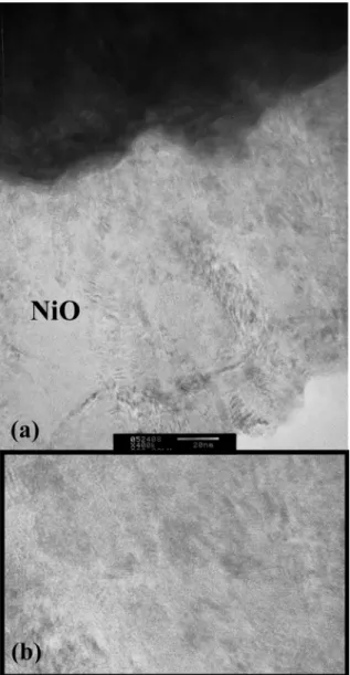
Results Fig. 2(a) shows the microstructure of the film with an O ratio about 56%. We found that the surface of our film was quite rough, and the interface between NiO and electrode was also very rough. As an example, Fig. 2(b) shows the enlarged part of the NiO film. It is obvious to observe that the polycrystal were everywhere in our films. Hotovy et al. ob-served that NiO films with good crystallinity could be grown at substrate temperature of 150 and over [11]. This suggests that although we did not heat the samples during the fabrication process, the temperature of the films maybe increase by sputter plasma deposition process. The effect of the polycrystal to the resistance bistability and the switching effect of NiO films is under processio , and will be reported later.
Fig. 3 reveals the typical current-voltage sweeping measure-ments of NiO film with various oxygen partial pressures. The percentage number represents the oxygen flow ratio to total chemistries flow rate. The measurement sequence follows a double-sweeping curve: 0 V positive bias voltage 0 V negative bias voltage 0 V. The absolute current value for the reverse bias voltage was taken in order to clarify the semilog scale.
Obviously, all four samples with different oxygen flow ra-tios behave the hysteresis phenomenon that the double stable resistance states at a certain read voltage, such as 3 V, appear. Initially, all samples are at a high-resistance state. After a SET voltage applying (a positive bias voltage), the resistance state changes to a lower one. However, if a high enough negative RESET voltage is applied, the resistance state changes again to initial. Accordingly, we defined these bistable states as SET state (low resistance) and RESET state (high resistance).
Fig. 3 also reveals a little bit asymmetry for positive and nega-tive bias voltage behaviors. This asymmetry might be attributed to the different work functions of interfaces between electrode and memory material. Reference [12] gave a systematic expla-nation about that. According to Fig. 3, the maximum resistance ratio of SET state to RESET state was defined as the resistance window. These windows can be plotted as Fig. 4 with different oxygen flow ratios. A strong effect of oxygen flow ratio on the resistance window was found. The resistance window dramati-cally increases from X3 to X100 as increasing oxygen flow ratio
Fig. 2. (a) Microstructure of NiO film with anO =Ar + O ratio of about 56%. (b) Enlarged part of NiO film.
Fig. 3. Current–voltage measurement (I–V curve) of NiO film with various oxygen partial pressures.
from 33% to 43%. The dashed line (ratio of about 37%) shows the immediate transition.
LEE et al.: EFFECT OF OXYGEN CONCENTRATION ON CHARACTERISTICS OF NiO -BASED RESISTANCE RAM 941
Fig. 4. Effect of the oxygen flow ratio on the resistance window.
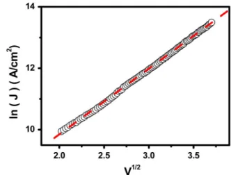
Fig. 5 shows the Schottky emission fitting of the current-voltage curve. The linear dependency indicates the transport mechanism is strongly dependent on the barrier height and the dielectric constant, as follows:
(1) where is the effective Richardson constant, is the bar-rier height, is the electric field, and is the insulator dielec-tric constant. The calculated dielecdielec-tric constants as well as the , defined as the barrier height difference between SET and RESET states by means of fitting the Schottky emission, were summarized in Fig. 6. A very high dielectric constant was gotten for the oxygen flow ratio of less than 33%. However, the oppo-site case can be observed for higher than 43%. The sample with a high dielectric constant means that it owns high charge storage capability. Because the electron transfer processes always ac-company the charge storage, the influence of dielectric constant becomes more important in MIM systems. Fig. 7 illustrates how the internal field affects the SET and RESET voltage for sam-ples of various oxygen flow ratios. If we pour the same voltage in two different permittivity samples, the real voltage in those samples will be different. For high permittivity sample, it can storage more charge in the interface and those charge form an opposite voltage in the insulator. Therefore, the real voltage in the sample was below the applied voltage. Similarly, there are few opposite voltage forms in the insulator of low permittivity sample. This might be explained due to the fact that the samples with few O ratios needed more voltage to switch the state.
Based on (1), the difference of the barrier height between SET and RESET states can be calculated, and the results are shown by the dashed curve plotted in Fig. 6. Clearly, the differ-ence of the barrier height behaves dramatic increasing around the oxygen flow ratio of 37%, which might correspond to the transition ratio shown in Fig. 4. As the O ratios in-creased, the change of barrier high also increased. According to those results, we could conclude that the value of resistance window should be dependent on the change of barrier height.
Fig. 8 shows the endurance measurement of NiO film with O ratios about 43%. In our measurement, the film
Fig. 5. Schottky emission approximation result. A clear V1/2 dependency means an Schottky thermionic emission.
Fig. 6. Dielectric constant as well as the barrier height with respect to the oxygen flow ratio.
Fig. 7. Dielectric constant and the barrier high change with various oxygen flow ratio. The left- and right-hand-side figures indicate the less and more oxygen flow ratio, respectively.
endures above eight hundred times of set and reset switching processes and those two states were not overlap. But with the increased switching times, the resistance increased in the switching processes. It might be attributed to the localized “burned” pits with crater-like geometry generated and the structure shorted [13]. For the resistance-increasing ratio of two states, the curve of two states will converge about 10 000 times switching processes.
942 IEEE TRANSACTIONS ON MAGNETICS, VOL. 43, NO. 2, FEBRUARY 2007
Fig. 8. Endurance measurement of NiO film withO =Ar + O ratios about 43%
III. SUMMARY
From this investigation, the bistable switching effect of NiO film was sensitive with the ratio of oxygen partial pressure to the working pressure. The samples with few O ra-tios needed more voltage to switch the state. The resistance window increased as the ratio increased. The optimum situa-tion is between 33% and 43%, and it shows a sudden jump in the resistance window. From the experimental data of NiO films, we have succeeded to demonstrate that the Schottky emis-sion function can be used to fit the permittivity and the change of barrier high with the different states. The samples of low O ratios own high permittivity, and it could be ex-plained that the samples with few O ratios needed more voltage to switch the state. The change of barrier high
of NiO films could be translated as the relation of resistance window and O ratios. It is the first time that the switching processes in oxide metal films can endure more than eight hundred times.
ACKNOWLEDGMENT
The authors are grateful for the financial support from the nano-research project of Academia Sinica, National Science Council of Taiwan, under Grant No. 95-2112-M-001-059, and the Macronix International Company, Hsinchu, Taiwan, R.O.C.
REFERENCES
[1] W. R. Hiatt and T. W. Hickmott, Appl. Phys. Lett., vol. 6, no. 106, 1965. [2] F. Argall, Solid-State Electron., vol. 11, no. 535, 1968.
[3] K. C. Park and S. Basavaiah, J. Non-Cryst. Solids, vol. 2, no. 284, 1970. [4] K. L. Chopra, J. Appl. Phys., vol. 36, no. 184, 1965.
[5] T. W. Hickmott, J. Vac. Sci. Technol., vol. 6, no. 828, 1969. [6] J. F. Gibbons and W. E. Beadle, Solid-State Electron., vol. 7, no. 785,
1964.
[7] A. Beck, J. G. Bednorz, Ch. Gerber, C. Rossel, and D. Widmer, Appl.
Phys. Lett., vol. 77, no. 139, 2000.
[8] S. Q. Liu, N. J. Wu, and A. Ignatiev, Appl. Phys. Lett., vol. 76, no. 2749, 2000.
[9] G. Dearnaley, A. M. Stoneham, and D. V. Morgan, Rep. Prog. Phys., vol. 33, no. 1129, 1970.
[10] S. Seo, M. J. Lee, D. H. Seo, S. K. Choi, D.-S. Suh, Y. S. Joung, I. K. Yoo, I. S. Byun, I. R. Hwang, S. H. Kim, and B. H. Park, Appl. Phys.
Lett., vol. 86, no. 093509, 2005.
[11] I. Hotovy, J. Huran, J. Jani’ka, and A. P. Kobzev, Vacuum, vol. 51, no. 157, 1998.
[12] J. R. Contreras, H. Kohlstedt, U. Poppe, and R. Waser, Appl. Phys. Lett., vol. 83, no. 4595, 2003.
[13] C. Rossel, G. I. Meijer, D. Bremaud, and D. Widmer, J. Appl. Phys., vol. 90, no. 2892, 2001.