Improvement in efficiency droop of GaN-based light-emitting diodes
by optimization of active regions
C.H. Wang, D.W. Lin, C. H. Chiu, S. P. Chang, Z. Y. Li, J. C. Li, H. C. Kuo, T. C. Lu, S. C. Wang
Department of Photonics and Institute of Electro-Optical Engineering,
National Chiao Tung University, Hsinchu 30010, Taiwan
ABSTRACT
We had demonstrated several novel methods to improve efficiency droop behavior in GaN-based light-emitting diodes (LEDs). LEDs with different kinds of insertion layers (ILs) between the multiple quantum wells (MQWs) layer and n-GaN layer were investigated. By using low-temperature (LT, 780。C) n-GaN as IL, the efficiency droop behavior
can be alleviated from 54% in reference LED to 36% from the maximum value at low injection current to 200 mA, which is much smaller than that of 49% in LED with InGaN/GaN short-period superlattices (SPS) layer. The polarization field in MQWs is found to be smallest in LED with InGaN/GaN SPS layer. However, the V-shape defect density, about 5.3×108 cm-2, in its MQWs region is much higher than that value of 2.9×108 cm-2 in LED with LT n-GaN
layer, which will lead to higher defect-related tunneling leakage of carriers. Therefore, we can mainly assign this alleviation of efficiency droop to the reduction of dislocation density in MQWs region rather than the decrease of polarization field. At second part, LEDs with graded-thickness multiple quantum wells (GQW) was designed and found to have superior hole distribution as well as radiative recombination distribution by simulation modeling. Accordingly, the experimental investigation of electroluminescence spectrum reveals additional emission from the previous narrower wells within GQWs. Consequently, the efficiency droop can be alleviated to be about 16% from maximum at current density of 30 A/cm2 to 200 A/cm2. Moreover, the light output power is enhanced by 35% at 20 A/cm2.
Keywords: light-emitting diodes, efficiency droop, active region design 1. INTRODUCTION
In recent years, great efforts have been made to improve the performance of GaN-based light emitting diodes (LED) due to their widespread application in solid-sate lighting, display technology, color printing, and optical storage1. One of
the promise approaches is to introduce an additional layer, such as InGaN/GaN short-period superlattices (SPS)2, 3,
InGaN layer4, 5, or low-temperature (LT) n-GaN layer6, between the n-type GaN and the multiple quantum wells (MQWs)
layers. Several studies have been revealed that such insertion layers (ILs) can release the residual strain in MQWs layer, reduce the V-pits density in MQWs, or improve the current spreading in LED2-6. As a result, the quantum efficiency and
the output power of LED can be enhanced. However, as the efficiency of LEDs increasing, the upcoming challenge is the efficiency “droop” for high-power applications7. It means that the efficiency reduces rapidly when LED operating
under high carrier density. The major cause of efficiency droop is still a huge controversy. Various possible mechanisms of droop including carrier overflow8, non-uniform distribution of holes9, 10, Auger scattering11, carrier delocalization12
have been proposed. Considering the advantages of using the ILs mentioned above, one can expect that the efficiency droop behavior can be alleviated in such LEDs with the ILs. But which kind of IL can reduce the efficiency droop more effectively? And what is the major mechanism for this reduction? More detailed investigations are necessary. Moreover, great efforts have been made to reduce the efficiency droop in recent years. Most of them are focus on minimizing the carrier overflow by reducing or eliminating the polarization field in the active region, such as using polarization-matched multiple quantum wells (MQWs)13, 14, staggered InGaN quantum wells15, and non-polar or semi-polar GaN substrate16.
But for improving hole distribution, only several approaches, such as p-type MQWs17 or coupled quantum wells18, are
explored. However, in the p-type MQWs, the Mg-dopant is very likely to diffuse into wells, while in the coupled quantum wells, electrons are tend to overflow by using thin barriers. These will result in reduction of radiative efficiency.
In this research, efficiency droop behaviors in GaN-based LEDs with different insertion layers between MQWs and
n-GaN and LEDs with graded-thickness multiple quantum wells (GQWs) were investigated.
2. CHARACTERISTICS OF EFFICIENCY DROOP IN GAN-BASED LIGHT EMITTING DIODES WITH AN INSERTION LAYER BETWEEN THE MULTIPLE QUANTUM WELLS
AND N-GAN LAYER
In this work, we studied the characteristics of efficiency droop in GaN-based LEDs with different kinds of ILs by performing the electroluminescence (EL), photoluminescence (PL), cathodoluminescence (CL), scanning electron microscope (SEM), and transmission electron microscopy (TEM) measurements.
2.1 Experiments
The samples in this study were grown on c-plane (0001) sapphire substrates by metalorganic chemical vapor deposition (MOCVD). After depositing a 20-nm-thick LT (550。C) GaN nucleation layer on the sapphire substrate, a
2-μm undoped GaN and a 2-2-μm Si-doped (5×1019 cm-3) n-type GaN were grown at 980。C, followed by an IL and the
MQWs active region. Two kinds of ILs were used in this study. One is InGaN/GaN SPS layer, which consisted of 10 pairs of In0.06Ga0.94N layer (~0.9 nm) and GaN layer (~1.7 nm). The other is 60-nm LT n-GaN layer. Note
that both of the ILs are doped with Si (5×1018 cm-3) and deposited at 780。C. The MQWs active region consisted of six
pairs of GaN barrier (~14.2 nm, deposited at 860。C) and unintentionally doped In0.15Ga0.85N well (~3.9 nm, deposited at
780。C). Finally, a 20-nm electron blocking layer with Mg-doped p-type Al0.15Ga0.85N and a 200-nm Mg-doped p-type
GaN layer were grown at 880。C. The Mg-dopant concentration is about 1×1019 cm-3. For comparison, the same LED
structure without the IL was also prepared. After growth, the LED chips were fabricated by regular chip process with ITO current spreading layer and Ni/Au contact metal, and the size of mesa is 300×300 μm2. Throughout this work, for
convenience, we shall refer to LED structures without and with InGaN/GaN SPS and LT n-GaN ILs as reference, type I, and type II LEDs. In addition, in order to investigate the surface morphology of MQWs, three samples without the electron blocking layer and the p-type GaN layer were also grown, denoted as reference, type I, and type II MQWs. 2.2 Results and Discussion
The electrical and luminescence characteristics of the LEDs were measured at room temperature (RT) with a calibrated integrating sphere. To prevent the self-heating effect, the devices were driven in pulsed mode with 1KHz frequency and 0.1% duty cycle. Figure 1(a) shows the output power of the three types of LEDs as a function of injection current. With 20-mA injection current, the output power of type I and type II LEDs are 18.0 and 17.0 mW, respectively, which are increased by 18% and 11%, as compared with the value of 15.3 mW for reference LED. While the enhancements at 200 mA are approximately 28% and 39% for type I and type II LEDs, respectively. These results indicate that not only the light output power has been improved but also the efficiency droop behavior has been changed by using the ILs. To illustrate the droop behavior more clearly, the normalized relative efficiencies of the three types of LEDs are plotted as a function of injection current in Fig.1 (b). Then, the efficiency droop can be defined as (ηpeak - η200 mA)/ηpeak, where ηpeak is the maximum efficiency at low injection current. It is interesting that the efficiency droop in type
II LED is only about 36%, which is much smaller than that in type I LED (49%) and reference LED (54%). That is, the efficiency droop behavior can be alleviated more effectively by using the LT n-GaN IL.
To figure out the origins of the alleviation in efficiency droop for LEDs with ILs, the power-dependent PL measurements excited with a frequency-doubled Ti: sapphire laser at wavelength of 385 nm were firstly carried out at RT. The laser pulse width was 200 fs and the repetition rate was 76 MHz. The laser beam was focused to a spot with diameter of 50 μm. The luminescence spectrum was dispersed by a 0.5 m monochromator and detected by a PMT tube. Figure 2 illustrates the emission energy and full width at half maximum (FWHM) as a function of excitation power. At an excitation power of 0.02 mW, the emission energies for type I and type II LEDs are 2.819 and 2.815 eV, respectively, which is much higher than that of 2.774 eV for reference LED. Meanwhile, the emission energies blue shift with increasing the excitation power in all of the three types of LEDs. Such blueshift can be attributed to two mechanisms: one is the photoinduced carriers screening effect of the polarization field accompanied by shrinkage of FWHM, the other is the band filling effect with a broadening of FWHM 19, 20. As can be seen from Fig.2 (b), the FWHM changes slightly in
the low excitation power range (<10 mW), indicating the screening effect is dominated in this region. As the excitation power is further increased, the band filling effect becomes dominated because of the significant broadening of FWHM.
Therefore, we analyzed semi-quantitatively the polarization field by fitting the emission energy of PL spectrum (hυ) in the low excitation power range with a triangular well model19:
3 / 2 3 / 1 3 / 1
(
)]
2
8
9
][
)
1
(
)
1
[(
)
(
)
(
F
n
m
m
n
dF
n
E
h
h e gh
π
υ
=
−
+
+
, (1)where the band-gap renormalization and the screening of the polarization field due to nonequilibrium carriers (n) are taken into account as Eg(n)=Eg(0)-βn1/3, and F(n)=F(0)-ned/εε0, respectively. Here, Eg(0), F(0) are the energy band-gap
and polarization field in the unexcited sample (n=0), respectively. While d, ε, and me,h are the well width, dielectric
constant, and electron- or hole-effective mass. In the calculation, the material parameters are obtained from the literature21, and the excitation power is converted into carrier density using the similar method in ref. 14. The fitting
results are illustrated in Fig. 2(a) by the dashed line. The F0 in the reference LED is found to be about 1.21 MV/cm,
which is lower than the value (1.87 MV/cm) obtained in similar MQW structure19. It can be attributed to that our MQWs
were grown on thicker n-GaN layer with lower residual strain22. But for type I and type II LEDs, smaller values are
obtained to be 0.62 and 0.66 MV/cm, respectively, implying both two kinds of ILs can release the residual strain for a certainty. The strain reduction effect by ILs has been studied and can be attributed to the suppression of the epiwafer bowing23. In addition, the InGaN/GaN SPS IL was demonstrated to decrease the epiwafer bowing more effectively,
resulting in larger a-axis lattice constant of GaN and lower compressive strain in MQW. This agrees with our experimental results.
It is well known that, the reduction of polarization field in InGaN/GaN MQWs cause less band bending, which in turn, results in higher emission energy, higher radiative recombination, and less electron leakage from the active region20, 24. Therefore, it is reasonable that type I LED has the highest light output power at 20 mA and the largest emission
energy, due to the smallest polarization field in it. However, it is still difficult to understand why the type II LED, instead of type I LED, does have a rather small efficiency droop.
Further insight investigations were performed by CL and TEM measurements. Although dark spots can be observed on the surface of all three samples from the monochromatic spatially resolved CL images (not shown here), the density is found to be decreased from 5.9-7.5×108 cm-2 in reference MQWs to 5.3×108 cm-2 and 2.9×108 cm-2, for type I and type
II MQWs respectively. The fluctuation of the value for reference MQWs is due to that some of the dark spots are overlap each other and difficult to figure out. Such dark spots are related to nonradiative centers in the V-defects confirmed by SEM morphology, which is commonly believed to consist of a threading dislocation terminated by a pit in the shape of an inverted hexagonal pyramid20, 21. In this sense, the lower dark-spot density suggests the reduction of dislocation
density in the MQWs region of both LEDs with ILs.
It has been reported that strain in the MQWs and In distribution inhomogeneities in the InGaN well are the main factors responsible for the V-defect occurrence and propagation25, 26. As discussed above, for type I LED, the strain in
the MQWs is relatively small. However, from the cross-section high resolution TEM (HRTEM) image in Fig 4 (a), one can clearly see slight well width and composition fluctuations in SPS layer. These may not only induce additional V-defects but also influence the subsequent growth of the MQWs layer. It is practical that type I MQWs exhibits rather rough interfaces and apparent non-uniformity of In distribution, as shown in Fig. 4 (b). While for the type II MQWs (Fig. 4 (c)), since the LT n-GaN IL does not contain In, clear and sharp interfaces can be observed. In addition, the In distribution is more homogeneous especially for the first and the second wells. Therefore, the dislocation density is much lower in the MQWs region of type II LED. Accordingly, the tunneling leakage of carriers from the QW to defect states in barriers is expected to be much smaller in type II LED than that in type I LED, which is considered to be one of the major reasons for the efficiency droop27. As a result, the efficiency droop behavior is alleviated more effectively by
Fig.1. (a) The output powers and (b) the normalized relative efficiencies for the three types of LEDs as a function of injection current. Fig.2. (a) The emission energy and (b) full width at half maximum for the three types of LEDs as a function of excitation power. Fig.3. CL images for (a) the SPS layer in type I LEDs, (b) MQWs structures in type I LEDs, and (c) MQWs structures in type II LEDs.
Fig.4. Cross-section high resolution TEM images for (a) the SPS layer in type I LEDs, (b) MQWs structures in type I LEDs, and (c) MQWs structures in type II LEDs.
2.3 Conclusion
In summary, the efficiency droop behaviors in two types of GaN-based LEDs with InGaN/GaN SPS and LT n-GaN ILs, respectively, were investigated in this work. The power-dependent PL reveals that the polarization field in MQWs is smallest in LED with InGaN/GaN SPS IL. Therefore, the output power at 20 mA (18.0 mW) is a little higher than that in LED with LT n-GaN IL (17.0 mW). However, the CL images indicate that the dislocation density in MQWs is much lower in the latter LED. This might be due to that the In distribution is more homogeneous and the interface in the MQWs is extremely sharp after inserting LT n-GaN layer, which is verified by the TEM image. Accordingly, the tunneling leakage of carriers from the QW to defect states in barriers is expected to be much smaller in LED with LT n-GaN IL. As a result, the efficiency only drops about 36% from the maximum value at low injection current to 200 mA, which is much smaller than that of 49% in LED with InGaN/GaN SPS IL and 54% in reference LED.
3. EFFICIENCY DROOP ALLEVIATION IN INGAN/GAN LIGHT-EMITTING DIODES BY GRADED-THICKNESS MULTIPLE QUANTUM WELLS
In this part, we designed and grew a LED structure with graded-thickness multiple quantum wells (GQWs) by using metal-organic chemical vapor deposition (MOCVD). Better hole distribution in such graded-thickness designed MQWs were demonstrated by APSYS simulation as well as the electroluminescence (EL) measurements. As a result, the efficiency droop behavior was alleviated while the radiative recombination was improved.
3.1 Experiments and Results
The LED structures were grown on c-plane sapphire substrates by MOCVD. A 20-nm-thick low temperature GaN nucleation layer followed by a 4 μm n-type GaN buffer layer, ten-pair InGaN/GaN superlattice were grown on the top of sapphire. After that, six-pair MQWs were grown with 10-nm-thick GaN barriers. For our designed experiment, the thicknesses of In0.15Ga0.85N quantum wells for GQW LED structure, controlled by growth time, are 1.5, 1.8, 2.1, 2.4, 2.7,
3 nm along [0001] direction. While the reference LED structure has a unique well-thickness of 2.25 nm. It’s worth noting here that the total volumes of active region for the two samples are the same. Finally, a 20-nm-thick electron blocking layer with Al0.15Ga0.85N and a 200-nm-thick p-GaN layer were grown to complete the epi-structure. For EL
measurements, the LED chips were fabricated by regular chip process with ITO current spreading layer and Ni/Au contact metal, and the size of mesa is 300×300 μm2.
It has been reported that, with the same indium content, wider well has longer radiative recombination lifetime28, 29.
In our designed GQWs, the well-thickness gradually increases along [0001] direction. Therefore, one can expect that the holes in wider well tend to escape to the next narrower well before they radiatively recombine with electrons, leading to the hole concentrations decrease in the wider well, but increase in the narrower wells. In other words, the hole
distribution will be improved. To prove the above hypothesis, we investigate the carrier distribution of both GQW and reference LED structures mentioned above by APSYS simulation.
Based on our experimental structures, we built up the model of the reference and GQW LED structures. The typical LED structure was composed of 4-μm-thick n-type GaN layer (n-doping=2×1018 cm-3), six pairs of In
0.15Ga0.85N/GaN
MQWs with 10-nm-thick GaN barriers, 20-nm-thick p-Al0.15Ga0.85N electron blocking layer (p-doping=5×1017 cm-3), and
200-nm-thick p-type GaN layer (p-doping=1×1018 cm-3). Other material parameters of the semiconductors used in the
simulation can be found in Ref. 30. Commonly accepted Shockley-Read-Hall recombination lifetime (several nano-seconds) and Auger recombination coefficient (2×10-30 cm6/s) are used in the simulations. Figure 5 shows the simulated
hole distribution and radiative recombination distribution along MQWs at 100 A/cm2. For reference LED structure, it
can clearly be seen that holes mostly concentrate in the QW nearest p-side (denoted as the first QW), so does the radiative recombination. This phenomenon coincides with the optical measurement result in ref. 31, which is mainly due to poor transportation of holes. While in the case of GQW LED structure, the hole concentration decreases in the first QW by about 16%, but increases in the second, third, and fourth QWs by 7%, 94%, and 175%, respectively, as compared with reference LED. It indicates that the holes are more capable of transporting across the first QW, consisted with our hypothesis. On the other hand, electrons are relatively not being affected due to their high mobility. Therefore, more wells will participate in the recombination process, as illustrated by the radiative recombination distribution in Fig. 5(b). Accordingly, the simulated EL spectrum of GQW LED at current density of 100A/cm2 exhibits lager full width at
half maximum (FWHM) than that of reference LED, as shown in the inset of Fig. 5 (b). Moreover, due to the relative low carrier densities in the first QW and more uniform of carrier distribution, the possibility of Auger scattering and carrier overflow can be lower. And the alleviation of efficiency droop can be expected..
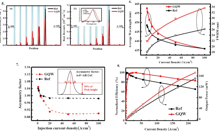
Figure 6 shows the power-dependent EL average wavelength and FWHM of reference and GQW LED at room temperature. The EL measurement was performed by on-wafer probing with a spectrometer. The emission wavelength (457.7 nm at 1 A/cm2) and FWHM (21.9 nm at 1 A/cm2) for GQW LED are larger than those for reference LED (448.5
nm and 17.9 nm), respectively. It could be due to the graded-thickness and wider wells near to p-side in GQW. Besides, as increasing the injection current from 1 A/cm2 to 100 A/cm2, EL spectrum for GQW LED exhibits significant blueshift
of 21.8 nm and broadening of about 11.6 nm, compared with 12.6 nm and 8.2 nm, respectively, for reference LED. Generally, the blueshift of the GaN-based LED can be attributed to the band filling effect in localized states and the charge screening effect of quantum confined Stark effect (QCSE)32. And the broadening of FWHM is mainly due to the
band filling effect and self-heating effect. In GQW and reference LEDs, the band filling effect and self-heating effect can be considered to be equivalent because they have the same indium content and total volumes of active region. Thus, there must be other reasons for such significant blue shift and broadening of EL spectra in GQW LED.
According to the simulated results mentioned above, more holes distribute in the narrower wells in GQW LED structure. Once more carriers radiatively recombine in narrower wells, the intensity of shorter-wavelength part in emission spectrum will rise. Thus, changes in symmetry of spectrum could be expected. To investigate the symmetry of EL spectrum in detail, the asymmetry factor (AsF) was calculated. As illustrated the inset of Fig.7, it can be defined as the distance from the center line of the peak to the back slope (AB) divided by twice the distance from the center line of the peak to the front slope (2AC), with all measurements made at 50% of the maximum peak height. The calculated AsF under every injection level for both samples are summarized in Fig. 7. It can clearly be seen that, AsF of reference LED decreases slightly from 1.04 to be about 0.98 when injection current increases from 1 A/cm2 to 100 A/cm2. While GQW
LED showes larger variation, the AsF starts at 1.05 (0.1 A/cm2) and saturates at about 0.89 (after 20 A/cm2). According
to the definition of AsF, if the bluer light emits from narrower wells, the symmetry of spectrum would be interrupted and smaller than 1. Therefore, we can conclude that GQW does have superior radiative recombination distribution, which leads to the EL spectrum blueshifts and broadens significantly with increasing the injection current. These enormous changes in wavelength and linewidth might make the design of the GQW concept impractical for lighting applications. In the future, we will optimize the GQW structure, such as appropriately reducing the indium content of the wider wells, to alleviate these effects.
Finally, we investigated the efficiency droop behaviors in both LEDs. The output powers measured with a calibrated integrating sphere and the normalized efficiency (η) of refrence and GQW LED are plotted in Fig. 8 as a function of injection current density. The light output power of GQW LED is found to be enhanced by 35 % at 20 A/cm2, as
compared with the reference LED (24.3 mW versus 18.0 mW). This indicates that even with wider wells (worse wave function overlap for electrons and holes) near p-side, the overall efficiency for GQW LED is still higher than reference, and the utilization rate of MQWs is improved. More importantly, the maximum efficiency (ηpeak) of GQW LED appears
efficiency droop, defined as (ηpeak - η200 Acm-2)/ηpeak, is alleviated from 32% in reference LED to 16% in GQW LED. This
improvement could be mainly attributed to the superior hole distribution and radiative recombination distribution, and also the reduction of Auger scattering resulting from the lower carrier concentration in QW nearest p-side.
Fig. 5. Simulated (a) hole distribution and (b) radiative recombination distribution in reference and GQW LEDs. Fig 6. Average wavelength and FWHM as a function of current density for reference and GQW LEDs. Fig. 7. Current-dependent asymmetry factor of electroluminescence spectra of reference and GQW LEDs. Fig. 8. Comparison of normalized electroluminescence efficiency and L-I curves
3.2 Conclusion
In conclusion, InGaN/GaN LEDs with graded-thickness multiple quantum wells were investigated both experimentally and numerically. The APSYS simulations indicate that superior hole distribution can be achieved in the GQW designed MQWs, in which the well-thickness increases along [0001] direction. It might be attributed to the longer radiative recombination lifetime in the wider well nearest to p-type layer. Moreover, by analyzing the EL spectra in detail, the additional emission from the narrower wells were demonstrated. This indicates that more carriers distribute in the previous wells, which agrees well with the simulated results. As a result, the efficiency droop behavior was alleviated from 32% in reference LED to 16% in GQW LED. In addition, the light output power was enhanced from 18.0 mW to 24.3 mW at 20 A/cm2 compared to reference LED with the same active volume. This work implies that with suitable
active region design, carrier transportation behavior could be modified, which is very useful for alleviating efficiency droop.
4. SUMMARY
We have demonstrated reduction of efficiency droop in GaN-based LEDs by using low temperature n-GaN insetion layer and graded-thickness MQWs. The efficiency of LEDs with LT n-GaN ILs only drops about 36% from the
maximum value at low injection current to 200 mA, which is much smaller than that of 49% in LED with InGaN/GaN SPS IL and 54% in reference LED. Moreover, with GQW structure, droop behavior could be further alleviated to 16%. These works imply that with suitable active region design, strain and crystal quality in active region and carrier transportation behavior could be modified, which is very useful for alleviating efficiency droop.
REFERENCES
[1] S. Nakamura, S. Pearton and G. Fasol, The blue laser diode: GaN based light emitters and lasers, 2nd ed. (Springer, New York, 2000), pp. 1-9.
[2] P. C. Tsai, Y. K. Su, W. R. Chen, and C. Y. Huang, Jpn. J. Appl. Phys., 49, 04DG07 (2010)..
[3] S. J. Leem, Y. C. Shin, K. C. Kim, E. H. Kim, Y. M. Sung, Y. Moon, S. M. Hwang, and T. G. Kim, J. Cryst. Growth, 311, 103 (2008).
[4] T. Akasaka, H. Gotoh, T. Saito, and T. Makimoto, Appl. Phys. Lett., 85, 3089 (2004).
[5] C. H. Jang, J. K. Shey, C. M. Tsai, S. J. Chang, W. C. Lai, M. L. Lee, T. K. Ko, C. F. Shen, and S. C. Shei, IEEE J. Quantum Elect., 46, 513 (2010).
[6] R. M. Lin, Y. H. Lin, C. H. Chiang, M. J. Lai, Y. L. Chou, Y. C. Lu, S. Y. Kuo, B. R. Fang, and M. C. Wu, Microelectron. Reliab., 50, 679 (2010).
[7] M. H. Kim, M. F. Schubert, Q. Dai, J. K. Kim, E. F. Schubert, J. Piprek, Y. Park, Appl. Phys, Lett. 91. 183507 (2007).
[8] K. J. Vampola, M. Iza, S. Keller, S. P. DenBaars, and S. Nakamura, Appl. Phys, Lett. 94, 061116 (2009).
[9] K. Ding, Y. P. Zeng, X. C .Wei, Z. C. Li, J. X. Wang, H. X. Lu, P. P. Cong, X. Y. Yi, G. H.Wang, J. M. Li, Appl Phys B, 97, 465–468 (2009).
[10] C. H. Wang, J. R. Chen, C. H. Chiu, H. C. Kuo, Y. L. Li, T. C. Lu, and S. C. Wang, IEEE Photon. Technol. Lett. 22, 236 (2010).
[11] A. David and M. J. Grundmann, Appl. Phys, Lett. 96, 103504 (2010). [12] B. Monemar and B. E. Sernelius, Appl. Phys. Lett. 91, 181103 (2007).
[13] M. F. Schubert, J. Xu, J. K. Kim, E. F. Schubert, M. H. Kim, S. Yoon, S. M. Lee, C. Sone, T. Sakong, and Y. Park, Appl. Phys. Lett. 93, 041102 (2008).
[14] Y. K. Kuo, J. Y. Chang, M. C. Tsai, and S. H. Yen, Appl. Phys. Lett. 95, 011116 (2009). [15] R. A. Arif, Y. K. Ee, and N. Tansu, Appl. Phys. Lett. 91, 091110 (2007).
[16] S. C. Ling, T. C. Lu, S. P. Chang, J. R. Chen, H. C. Kuo, and S. C. Wang, Appl. Phys. Lett. 96, 231101 (2010). [17] J. Xie, X. Ni, Q. Fan, R. Shimada, Ü. Özgür, and H. Morkoç, Appl. Phys. Lett. 93, 121107 (2008).
[18] X. Ni, Q. Fan, R. Shimada, Ü. Özgür, and H. Morkoç, Appl. Phys. Lett. 93, 171113 (2008).
[19] E. Kuokstis, J. W. Yang, G. Simin, M. A. Khan, R. Gaska, and M. S. Shur, Appl. Phys. Lett. 80, 977 (2002). [20] T. Wang, D. Nakagawa, J. Wang, T. Sugahara, and S. Sakai, Appl. Phys. Lett. 73, 3571 (1998).
[21] U. M. E. Christmas, A. D. Andreev, and D. A. Faux, J. Appl. Phys., 98, 073522 (2005).
[22] L. T. Romano, C. G. Van de Walle, J. W. Ager III, W. Götz, and R. S. Kern, J. Appl. Phys., 87, 7745 (2000). [23] M. Sakai, T. Egawa, M. Hao, and H. Ishikawa, Jpn. J. Appl. Phys. 43, 8019 (2004).
[24] F. D. Sala, A. D. Carlo, P. Lugli, F. Bernardini, V. Fiorentini, R. Scholz, and J. M. Jancu, Appl. Phys. Lett. 74, 2002 (1999).
[25] I. H. Kim, H. S. Park, Y. J. Park, and T. Kim, Appl. Phys. Lett. 73, 1634 (1998).
[26] D. I. Florescu, S. M. Ting, J. C. Ramer, D. S. Lee, V. N. Merai, A. Parkeh, D. Lu, E. A. Armour, and L. Chernyak, Appl. Phys. Lett. 83, 33 (2003).
[27] N. I. Bochkareva, V. V. Voronenkov, R. I. Gorbunov, A. S. Zubrilov, Y. S. Lelikov, P. E. Latyshev, Y. T. Rebane, A. I. Tsyuk, and Y. G. Shreter, Appl. Phys, Lett. 96, 133502 (2010).
[28] C. K. Sun, S. Keller, T. L. Chiu, G. Wang, M. S. Minsky, J. E. Bowers, S. P. Denbaars, IEEE J. Sel. Top. Quantum Electron. 3, 731 (1997).
[29] R. Charash, P. P. Maaskant, L. Lewis, C. McAleese, M. J. Kappers, C. J. Humphreys, and B. Corbett, Appl. Phys. Lett. 95, 151103 (2009).
[30] F. Bernardini, in Nitride Semiconductor Devices: Principles and Simulation, edited by J. Piprek (Wiley, New York, 2007), pp. 49-67.
[31]A. David, M. J. Grundmann, J. F. Kaeding, N. F. Gardner, T. G. Mihopoulos, and M. R. Krames, Appl. Phys. Lett. 92, 053502 (2008).
[32]T. Takeuchi, S. Sota, M. Katsuragawa, M. Komori, H. Takeuchi, H. Amano and I. Akasaki, Jpn. J. Appl. Phys. 36, L382 (1997).