Impact
of
Self-Heating Effect on Hot Carrier Degradation in High-Voltage LDMOS
Chih-Chang Cheng, J.F. Lin, Tahui Wang
Dept.
of Electronics Engineering, National
Chiao-Tung University, Hsin-Chu, Taiwan T.H. Hsieh, J.T. Tzeng, Y.C. Jong, R.S. Liou, Samuel C. Pan, and S.L. HsuTaiwan Semiconductor Manufacturing
Company, Science-Based Industrial Park, Hsin-Chu, Taiwan E-mail:twanggcc.nctu.edu.tw
Abstract Thedevice was processed in a 0.
18tm
CMOStechnologywithagateoxide thickness of100nmand a channel length of Self-heating induced transient hot carrier effects in high- 3m.TeorainvlgsaeVgOVndV4V.o3utm. The
operation
voltages
areVg=40V
andVd=40V.
Tovoltage
n-LDMOS areinvestigated.
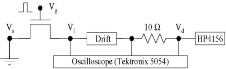
A novel LDMOS eliminate SUE inmeasurement, a fast transientmeasurementstructure incorporating a metal contact in the bird's beak '
region is
fabricated,
which^ allows us to probe an internal~~~~~~~~~~2.
stLincudring audiita oilloscopedis0built,
Linear drain
current(Id1m,@Vg/Vd=4OV/O.
1V) iS
as
shwnirFg
measured voltage transient in hot carrier stress. The AC stress-to
monitor devicedegradation
under AC/DC stress. A three-frequency dependence ofdevice degradation is characterizedregion charge pumping technique [3, 4]
is used to locate hot and evaluatedby
a two-dimensional numerical simulation. carrierdamage
area in the device and toidentify
thetype
ofOurresult shows that drain current degradation in AC stress g T d
is moreserious than in DC stress because of thereduction of performed to calculate a temperature
gerated
otaps.
T-mensiona disimution
distribution andisself-heating
effect.corresponding
hotcarrier
effects.Introduction
IVg Laterally diffused MOS (LDMOS) transistors have been
widely utilized in today's
high-voltage/high-current
driversVs
V
I0QVd
and RF power amplifiers [1,2]. Due to large power t t m S1
consumption, self-heating effect (SUE) is significant in a
LDMOS. In this paper, we will study
SUE
on hot carrier -Oscilloscope (Tektronix
5054) degradationin DC andAC stressmodes. Tothispurpose, wefabricate a special LDMOS structure, which incorporates a Fig. 2: Fast transient measurement setup for drain current and internal
metal contact inthe bird's beak region. Thus, we canprobe voltage (VI) characterization. The external resistance (1OQ) is negligible an internal voltage (VI) transient due to SUE directly. Fig. 1 compared to a total device resistance(40V/lOmA-4kQ). A gatepulseand
illustrates the device structure. Three regions of a LDMOS
constantVd
areapplied.are indicated in the figure, including a channel region, an
accumulationregion anda field-oxide region. The contactis Results and Discussion arranged inthe accumulationregion that the internal voltage
VI
can be used as a monitor for hot carrier effects in the (a)Self-HeatingCharacterization channel. The contact area is small enough that the deviceelectrical characteristics are notaffected. Fig. 3(a) shows a normalized draincurrent(Id/W) versus Vd in small and large gate width devices in DC (Agilent
G_
4156)
measurement. TheId/W
inalinearregion
isnearly
thesame, indicating no process variations in these two devices.
S
D
VI
DHowever,
thelarger
width device exhibits a smallerId/W
innFt the saturation region because oflarger power consumption
Y i N-Well and thusa
larger
SUE.
Thereduction of the saturationcurrent
is attributed to
self-heating
inducedmobility
degradation
ih
Lacc LfOX * * * e [5,6]. Fig. 3(b) compares the Id/W from a DCand from a fastLch Lacc Lfox transient measurement for the large width device. A larger
Id/W is noticed in the transient measurement because of the
Fig. 1: Cross-section of a novel LDMOSstructure. The metal contaCt(vI)is elimination of SUE. In addition, SUE is manifested in the
arranged in the accumulation region with a n+implant. Three regions are
indicated, including channel region (Lch), accumulation region (Lac), and internal voltage measurement results byAgilent4156 and by
field-oxide
region(LfQx).
ac, the fasttransient setup (Fig. 4). The larger VI in anon-SUEcondition is attributed to a higher mobility in accumulation stress modes. Max. IB stress shows a slight difference in
'dli
region, thus resulting in a smaller drift region resistance. A degradation between AC and DC stresses, implying that SUE larger internal voltage innon-SUE
condition implies a is not important at a lower stress Vg. However, in maximum strongerhot carrierstressinthe channel region. Ig stress, AC stress shows much moreIdlm
degradation than DC stress. Moreover, strongstress-frequency (Fig. 7(a)) and duty cycle (Fig. 7(b)) dependence is observed. In Fig. 7(a),. . . the Idim degradation increases with frequency and then
F
(a,
85%
s becomes saturated. Acorner
frequency is found to befr=20
kHZ at a duty cycle=10%. In Fig. 8, weplot
'di.
degradation T ,,,. versuspulse duration, i.e., duty cycle/frequency, inAC stress.<4 sF * *
W=20gm
A corner time of5gs
isobtained,
suggesting thatSUE
o . @ . becomesimportantaspulseduration islonger than -5gs.
_ .;
>r
*
~W=5RLm
~~~~~~~~~~~~~~~~~~~~~Max.
I
B
Max.
I-7 DCMeas. . . . d 5 O\6
t (b)
8.4%+
Vd 5OV
o__.-
* DC Meas. ] 0 10 20 30 40 50 -TransientMeas. Vg(V)
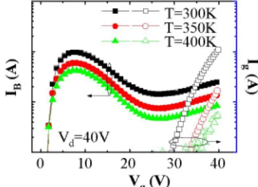
Fig. 5: Substrate current and gate current versus gate voltage in a LDMOS.
. /
W/L=20Oum/3,um
Two hot carrier stress modesareshown,maximumIBstress and maximumIg stress.0
10
20
30
408
Vd(V)8,
Vd ()
IDC
Stress
Fig. 3:(a) Normalized draincurrent(Id/W)versusdrainvoltageinsmall and AC Stress
largegatewidth devicesin DC measurement(Agilent 4156). (b) The Id/W fromaDCandafast transientmeasurementfor thelarge width device. -.
42
25
... . .[W/L=2
0
tm/3
ptm
l
F .\ Vd-~V 40Vi20
F-*[~ [\~ g - ]
Max. IB
Max.I
*SHE Fig. 6: Linear drain current degradation (Vg/Vd= 40V/0.lV) in two hot
15 - * DC Meas. carrier stress modes. DC and AC stresses have the same cumulative stress
time.AC stresshasafrequency of20kHzandaduty cycle of 10%.
_
Transient
Meas.
10 L- .
|(a)
l SW/L=20gm/3gm
(b) StressFrequency0
10
20
30
40
.o
*
@20kHz
vg
(V)
Fig.4:Internalvoltageversusgatevoltage measured by Agilent4156andby e 6
atransientmeasurementsetup.
(b) Degradation Characteristics inACIDCStress 1..* ,,
Duty',10%|
0.21 10 100
o
02 .9 1Two stress modes (max.
'B,
and max.'g)
are chosen in Stress Frequency(ktHZ)
Duty cyclethe study of hot carrier degradation in n-LDMOS. The Ig-Vg Fig. 7: (a)bmli degradation versus stress frequency with a duty cycle of10%o.
and IB-Vg of a n-LDMOS are shown in Fig. 5. Fig. 6 shows A corner frequency (fi ) is around 20kHz. (b)Idli degradation versus duty
AC and DC stress induced
'dim,
degradations in the above two cycle forafrequency
of20kHZ.
higher drift region resistance. The SHE is stronger at a higher 8 .Vg. The simulation also reveals a
higher
VI
in a non-SHE1ZDuty cycle condition (Fig. 13). Good agreement between measurement
U
10%0
and simulation is obtained in Fig. 13. Because of a largerVI
El
90%0
in the non-SHE condition, the simulated impact ionization6\
q rate is stronger in the non-SHE condition(Fig. 14).
Thisfeature also confirms our charge-pumping results in Fig. 10 and concludes a more serious
Idl,
degradation rate in AC_ ... . ,stress
,
,.
(Fig. 15).
.
. +,
4
1 10 100 1000 Duty Cycle / Frequency(gsec)
Fig. 8:I,1indegradation versus pulse duration(=duty cycle/frequency) in AC -1.6
stress. The corner time is around 5gts. Post DCStress
1
F S
~~~~~A-Post
AC Stress
Fig. 9 shows a
VI
transient in
a pulsed gate and DC
drain voltage condition. The
VI
decreases with time due toLfoxA
SUE
and the onsettime ofSUE
is extractedtobe around5gs.
_L This result is consistent with thefindings
from AC stressLacc
induced degradation (Fig. 8).
Lchan _. , . . I . L
___ __ __ __ __ __ __ __ __ __ ___ _____ 0
-32 -24 -16 -8 0
40
VgL
(V)
Fig. 10:Three-region charge pumpingmeasurementresults after maximum
. r
V 'g AC and DC stress. A VgL shift is in the accumulation region andalcp
i~30 [ W g 2 increase is in the channel region. For moredetails,see [3,4].
>) 1 T-300K
e5gs
T=350K20
V1
T=400K
10
0
20
40
60
80 100
/
Pulse
Time
(g
sec)
Vd=40V
Fig. 9: The internal voltage(VI) transient in apulsed gate andDC drain
voltage(Vd=40V) condition. The waveforms ofVI andVg areplotted. The 0 10 20 30 40
onsettime forSHEis 5s. g(V)
Fig.11: Substratecurrentandgate current versus gatevoltage for different
A charge pumping measurement
(Icp)
result is shown in temperatures.Fig. 10. A distinguished three-stage feature in cp
-VgL
isobserved, corresponding to the three regions of a LDMOS
L
tL
respectively. By comparing the pre-stress and post-stress
ICP
chVg=lOV
in each
stage,
we areable toseparate
interfacetrap
(Nit)
andfixed oxide
charge
(Qox)
creation ineachregion
of the device. 312The result in
Fig.
10reveals that ACstressgenerates
moreNit
CDin the channel region and more
Qox
in the accumulation i0region.
The larger trapgeneration
rate in AC stress results from a smallertemperature
rise and thus alarger
stressgate
current
(Fig.
11).
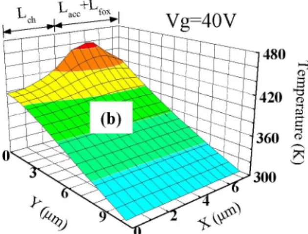
Theself-heating
inducedtemperature
304change
in a LDMOS is simulatedby
a two-dimensional 0numerical device simulation (Fig. 12). The ambient 6; 300
temperature in the simulation is 300K. In Fig. 12, the drift 9e
region
shows ahigher
temperature change than channel $region, implying a larger mobility degradation and thus a 0
L.h _+' 10_
Vg=40V
11
IO| S
Post
AC Stress
480
o=
[
*Post DC
Stress,
E91l
~~~~~~1
-t---d~~~~~~~~420
~~360C./
CDX
0~~~~~~~~~~~~~~~~~~~~~~~
---z >XXUX
13000
1110
1 ioStress Time
(sec)
Fig.15:Iui,degradationrateafter AC and DCstressinmaximum1gstress
condition.The AC stressfrequencyis20kHzandtheduty cycleis1O%. Fig. 12: Simulation of a temperature distribution with SHE. The ambient
temperature is 300K. X and Y axes are indicated in Fig. 1. (a)
Vg/Vc=lOV/40V.(b)Vg/Vch=40V/40V. Acknowledgments
6 The authors of NCTU would like to acknowledge
financial and technical support from NSC under contract #
4 - Transient Meas. NSC 95-2221-E-009-303 and TSMC JDP. The authors also
5 -a- Simulation would like acknowledge National Center for
High-Performance Computing for providing the device simulation
<2 environment.
0 V
d4V
,
References0 10 20 30 40
Vg(V) [1] D. Muller, A. Giry, F.Judong, C. Rossato,F. Blanchet, B. Szelag, A.
Fig.13:Internalvoltagechange(V(non-SHE)-VI(SHE))versusgatevoltage Monroy Aguirre, R. Sommet,D. Pache, and 0. Noblanc,
"High-frommeasurementand fromsimulation. Performance 15-V Novel LDMOS Transistor Architecture in a
0.25-,um
BiCMOSProcessforRF-PowerApplications,"IEEETrans.onElectronDevices,vol.54,pp.861-868,April,2007.
[2] Jongdae Kim,Tae MoonRoh, Sang-Gi Km,Q. Sang Song,Dae Woo ~~~~~~~ ~~~~~Lee,Jin-GunKoo,Kyoung-lk Cho,andDongSung Ma,"High-Voltage
l l l l l| l| Power Integrated Circuit Technology Using SOI for Driving Plasma Display Panels,"IEEE Trans. on ElectronDevices, vol. 48,
pp.1256-~ ~~~~~1263,June,2001.
[3] Chih-ChangCheng,K.C.Tu,TahuiWang,T.H.Hsieh,J.T.Tzeng,Y.C. Jong, R.S. Liou, Sam C. Pan, and S.L. Hsu, "Investigation ofHot CarrierDegradationModesinLDMO5byUsingaNovelThree-Region Charge Pumping Technque," IEEE International Reliability and
-IIllliiiiil 1 1 Physics Symposium(IRPS),pp.334-337, 2006.
Jong, R.S. Liou, Samuel C. Pan, and S.L. Hsu "Physics and Characterization of Various Hot CarrierDegradation Modes in LDMOS Fig.14:Twodimnsinaldevie smultio ofimpct iniztio geeraion byUsing aThree-Region Charge PumpingTechnique,"IEEE Trans. on
(JIG) rate at Vg/Vd=40V/40V. (a) SHE is included and (b) SHE is not Device and Materials Reliability,pp.358-1363,2006.
included. [5] Emil Arnold, Howard Pein, and Sam P. Herko, "Comparison of Self-Heating Effects In Bulk-Silicon and501 High-Voltage Devices," IEEE Conclusion International Electron Device Meeting(IEDM,),pp.8113-816, 1994.
[6] Gary M. Dolny, Gerald E. Nostrand, and Kevin E. Hill, "The Effect of
Transient self-heating effect in AC hot carrier stress in Temperature on Lateral DMOS Transistors in a Power IC Technology,"
LDMOS has been studied by measuring an internal voltage. IEEE Trans.on Electron Devices, vol. 39, pp.990-995, April, 1992. The extracted self-heating time is around
5gs.
The AC stressat maximum