0040-6090/01/$ - see front matter䊚 2001 Elsevier Science B.V. All rights reserved. PII: S 0 0 4 0 - 6 0 9 0 Ž 0 1 . 0 1 3 3 0 - X
The effect of ammonia plasma treatment on low-
k
methyl-hybrido-silsesquioxane against photoresist stripping damage
T.C. Chang
a,c,*, Y.S. Mor , P.T. Liu , T.M. Tsai , C.W. Chen , Y.J. Mei , S.M. Sze
b c b b d b,c Department of Physics, National Sun Yat-Sen University, Kaohsiung, Taiwan, ROCa
Institute of Electronics, National Chiao Tung University, Hsin-Chu, Taiwan, ROC
b
National Nano Device Laboratory, 1001-1 Ta-Hsueh Road, 300, Hsin-Chu, Taiwan, ROC
c
Department of Electrical Engineering, Ching-Yun Institute of Technology, Jung-Li, Taiwan, ROC
d
Abstract
The integration process, low-k hybrid-organic-siloxane-polymers (HOSP) and photoresist stripping process have been
investigated. The dielectric properties of HOSP films are degradated after photoresist removal. This is because photoresist stripping processes destroy the functional groups and induce moisture uptake in HOSP films. In this study, NH -plasma treatment was used3
for HOSP films to form a thin nitrogen-containing layer, preventing HOSP films from O plasma ashing and chemical wet stripper2
damage during photoresist removal. The leakage current is decreased significantly and the dielectric constant is maintained at a low value after photoresist removal. These experimental results show that NH treatment is a promising technique to enhance the3
resistance of HOSP films to the photoresist stripping process.䊚 2001 Elsevier Science B.V. All rights reserved.
Keywords: Ammonia; Hybird-organic-siloxane-polymer; Photoresist stripping
1. Introduction
As the critical dimension of integrated circuits is scaled down, the linewidth and spacings between metal interconnections are made smaller. A larger portion of the total circuit transmission time (i.e. RC delay) will
be from parasitic resistance and capacitance of the interconnections. The interconnection becomes a bottle-neck in improving the chip performance such as the speed and power consumption w1,2x.
In order to decrease the resistance (R), copper has recently been introduced as the interconnect metal, due to its high electrical conductivity (;1.8 mVcm) com-pared with 3.0 mVcm of Al. In addition, copper inter-connect possesses a higher resistance to electromigration than Al wiring by one to two orders of magnitude.
Low dielectric constant (low-k) materials also are proposed to decrease the parasitical capacitor w3–9x. One * Corresponding author. Tel.: 6100; fax: q886-3-572-2715.
E-mail address: [email protected](T.C. Chang).
of many low-k dielectrics, a spin-on deposition
hybird-organic-siloxane-polymer (HOSP) is a promising
can-didate. The HOSP film is a derivative of SiO in which2
one of the four oxygen atoms bonded to every silicon atom is replaced by hydrogen and methyl groups.
The HOSP is a SiO -based material, which is highly2
suitable for ULSI applications because of the low dielectric constant of approximately 2.5. Therefore, the integration of the HOSP films as an interlayer dielectric into multilevel interconnects has received much attention in recent years.
In integration processing, photoresist stripping is an indispensable step. The photoresist removal is common-ly implemented with O -plasma dry ashing and wet2
stripper solution dipping. The dielectric properties of the low-k films may be degradated during photoresist
stripping processes w10,11x.
In this work, we studied the NH -plasma treatment to3
improve the quality of HOSP films. Electrical measure-ment and material analyses have been used for evalua-tion. In addition, O -plasma ashing and wet stripper2
Fig. 1. FTIR spectra of HOSP films before and after a series of baking and curing steps.
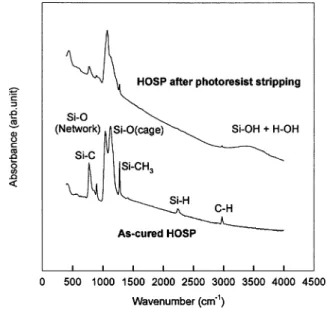
Fig. 2. FTIR spectra of HOSP films before and after photoresist strip-ping processes(O plasma ashing and wet stripper dipping).2
dipping have been investigated to determine the impact of integrated processes on the dielectric film quality.
2. Experimental
The substrates used in the study were 4-inch p-type single crystal wafers (resistivity: 15–20 Vcm) with
(100) orientation. The wafers were coated with the
HOSP methyl-hybrido-silsesquioxane(MHSQ) solution at rotational velocity 500 rev.y min for 5 s for the first
stage. Then, a second spinning stage was implemented at 2500 rev.y min for 20 s. After the spin-coating process,
the HOSP films were baked sequentially on a hot plate at 1508C, 2008C and 3508C for 1 min, respectively. It was followed by a furnace curing at 4008C under a nitrogen ambient for 1 h.
Four types of samples which were labeled as samples STD, NH-3, NH-6 and NH-9, respectively, were pre-pared. Sample STD was the as-cured HOSP film without any plasma treatment. Samples NH-3, NH-6 and NH-9 were the as-cured HOSP films with NH plasma pre-3
treatment for 3, 6 and 9 min, respectively. Then, all types of samples were treated with O plasma ashing2
for 3 min and wet stripper dipping at 608C for 10 min, respectively.
The NH3 plasma treatment was carried out in a plasma-enhanced chemical vapor deposition (PE-CVD)
chamber. The NH plasma was operated with a rf power3
of 200 W at a pressure of 300 mtorr. The flow rate was 700 sccm, and the operating temperature was kept at 3008C.
Metal insulation semiconductor capacitors (MIS) were manufactured by depositing aluminum onto the HOSP film as the top-electrode.
The chemical bonds of the HOSP films after different processes were investigated by Fourier transform
infra-red (FTIR) spectroscopy. The thickness of the HOSP
films were measured by a n&k analyzer. The capaci-tance–voltage (C–V) characteristic was measured at 1
MHz with an AC bias for high frequency. A Keithley Model 82 CV meter was used to make the measurements on an electrode area of 0.0053 cm . The current–voltage2
(I–V) characteristics were also measured using MIS
structure to evaluate the insulation property of HOSP film.
3. Results and discussion
Fig. 1 shows the FTIR spectra of HOSP films before and after a series of baking and curing steps. After 1508C, 2008C and 3508C baking, the intensity of Si–O
(cage) peak is decreased and Si–O–Si (network) peak
intensity is increased. After 4008C curing, the network structure significantly appears. It clearly shows that a large amount of Si–O bonds cross-link into Si–O–Si bonds and form a more rigid network structure.
In integrated processes, photoresist removal is an indispensable step. The photoresist removal is imple-mented conventionally by O plasma ashing and wet2
stripper solution treatment. Therefore, the impact of O2
plasma ashing and chemical wet stripper on the quality of HOSP film was investigated in this study. Fig. 2 shows the FTIR spectra of the as-cured HOSP film before and after photoresist removal processes (i.e. O2
plasma ashing and chemical wet stripping). The
inten-sities of Si–OH and H–OH bonds were increased after photoresist stripping. Furthermore, the intensities of Si–H, C–H and Si–CH peaks were decreased dramati-3
cally. These FTIR spectra results can be explained as follows.
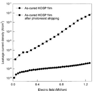
Fig. 3. The leakage current density of HOSP films before and after photoresist stripping processes.
Fig. 5. FTIR spectra of Samples STD, NH-3, NH-6 and NH-9 after photoresist stripping processes.
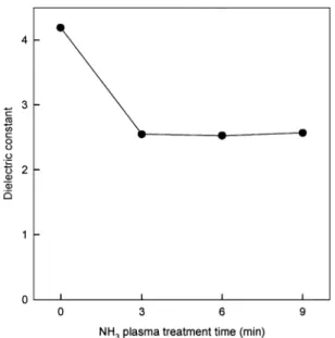
Fig. 4. The dielectric constant of HOSP films before and after pho-toresist stripping processes.
Fig. 6. Leakage current density of Samples STD, NH-3, NH-6 and NH-9 after photoresist stripping processes.
During O2 plasma ashing, O radicals react with functional groups of HOSP films, breaking Si–CH3
bonds and Si–H bonds. This causes the HOSP films to generate dangling bonds. Sequentially, the high-alkalin-ity content of wet stripper solution (pH 12.6) leads to continuous hydrolysis reactions of HOSP films, forming even more dangling bonds in the HOSP films. The dangling bonds could easily react with hydroxide ions
(OH ) in the wet stripper solution and form Si–OHy
bonds. These Si–OH bonds in the HOSP films lead to moisture uptake. Therefore, the Si–OH bond and H–OH bond signals appear in the FTIR spectra.
Fig. 3 shows the leakage current density of the HOSP films before and after photoresist removal. The leakage current increased after photoresist removal. The dielec-tric constant also increased significantly, as shown in Fig. 4. The dielectric loss is due to the destruction of functional groups in the HOSP films after photoresist removal, as shown in Fig. 2. In order to address these issues, NH plasma treatment was developed to enhance3
the resistance to photoresist stripping processing. Fig. 5 show FTIR spectra of NH3 plasma-treated HOSP films(i.e. samples NH-3, NH-6 and NH-9) after
photoresist stripping. It is found that all the intensity of functional groups still remained at a high level. Mean-while, Si–OH bonds and H–OH bonds did not appear in the FTIR spectra.
Fig. 7. Dielectric constant of Samples STD, NH-3, NH-6 and NH-9 after photoresist stripping processes.
Fig. 8. XPS diagram of as-cured and NH plasma-treated HOSP films.3
These leakage currents of NH plasma-treated HOSP3
films are much lower than that of untreated HOSP films after photoresist removal, as shown in Fig. 6. Moreover, the dielectric constants of NH plasma-treated HOSP3
films can still maintain a low-k value, as shown in Fig.
7.
Fig. 8a,b shows the XPS diagrams of as-cured and NH plasma-treated HOSP films, respectively. In con-3
trast to Fig. 8a, it is found that a significant signal of nitrogen appears at approximately 400 eV in Fig. 8b. This indicates that nitrogen atoms are doped in the HOSP films and form a thin nitrogen-containing layer on the NH plasma-treated HOSP surface.3
The thin nitrogen-containing layer generated from NH plasma is thought to be a barrier against photoresist3
stripping damage. The nitrogen-containing layers passi-vate dangling bonds on the HOSP surface and prevent moisture uptake. As a result, both the leakage current and dielectric constant of NH3 plasma-treated HOSP films will maintain low-k properties after photoresist
stripping.
4. Conclusions
In this study, NH -plasma treatment was applied to3
HOSP films. The NH plasma treatment transforms the3
HOSP surfaces into a thin nitrogen-containing layer. The nitrogen-containing layer is a good barrier against O2 plasma and high-alkalinity wet stripper solution attack. Material analyses verified our interpretation. The Si–OH bounds were not observed in the FTIR spectra when NH plasma-treated HOSP films underwent pho-3
toresist stripping processes. In addition, electrical meas-urements also show that the leakage current of NH3
plasma-treated HOSP films is decreased significantly
and the dielectric constant is maintained at a low-k
value.
Acknowledgements
This work was performed at the National Nano Device Laboratory and was supported by Honeywell Taiwan Inc. and the National Science Council of the Republic of China under Contract, No. NSC90-2215-E-110-001 and No. NSC89-2215-E-231-005.
References
w1x The National Technology Roadmap for Semiconductors,
Semi-conductor Industry Association, San Jose, CA, 1997.
w2x T.E. Seidel, C.H. Ting, Mater. Res. Soc. Symp. Proc. 381(1995)
3.
w3x P.T. Liu, T.C. Chang, Y.L. Yang, Y.F. Cheng, S.M. Sze, IEEE
Trans. Electron Devices 47(2000) 1733.
w4x M.G. Albrecht, C. Blanchette, J. Electrochem. Soc. 145(1998)
4019.
w5x M.J. Loboda, C.M. Grove, R.F. Schneider, J. Electrochem. Soc.
145(1998) 2861.
w6x S.W. Lin, M. Miyata, T. Naito, Y. Shimogaki, Y. Nakano, K.
Tada, H. Komiyama, Mater. Res. Soc. Symp. 443(1996) 143. w7x A. Grill, V. Patel, K.L. Saenger, C. Jahnes, S.A. Cohen, A.G.
Schrott, D.C. Edelstein, J.R. Paraszczak, Mater. Res. Soc. Symp. 443(1996) 155.
w8x S.M. Rossnagel, Proceedings of the VLSI Multilevel
Intercon-nection Conference(VMIC), 1995, p. 576.
w9x S. Okuda, Y. Shioya, H. Kashimada, Proceedings of the VLSI
Multilevel Interconnection Conference(VMIC), 1995, p. 424. w10x P.T. Liu, T.C. Chang, Y.S. Mor, S.M. Sze, Jpn. J. Appl. Phys.
38(1999) 3482.
w11x P.T. Liu, T.C. Chang, S.M. Sze, F.M. Pan, Y.J. Mei, W.F. Wu,
M.S. Tsai, B.T. Dai, C.Y. Chang, F.Y. Shih, H.D. Huang, Thin Solid Films 332(1998) 345.