New CMOS 2V low-power
IF fully
differential Rm-C
bandpass amplifier for
RF
wireless receivers
YCheng, J.Gong and C.-Y.Wu
Abstract: A new CMOS fully differential bandpass amplifier (BPA) based on the structure of a transresistance (Rm) amplifier and capacitor is proposed and analysed. In this design, the Rm amplifier is realised by a simple inverter with tunable shunt-shunt feedback MOS resistor and tunable negative resistance realised by crosscoupled MOS transistors in parallel with a current source. The capacitor is in series with the input of the Rm amplifier, which realises the filter function and blocks the DC voltage. Under a 2V supply voltage, the post-tuning capability of the gain can be as hgh as 55dB whereas the tunable frequency range is 41-178MHz. The power consumption is 14mW and the dynamic range (DR) is 50dB. The differential-mode gain is 20dB and the common-mode gain is -25dB so that the CMRR is 45dB. Simple structure, good frequency response and low power dissipation make the proposed bandpass amplifier quite feasible for application in the IF stage of R F receivers.
1 Introduction
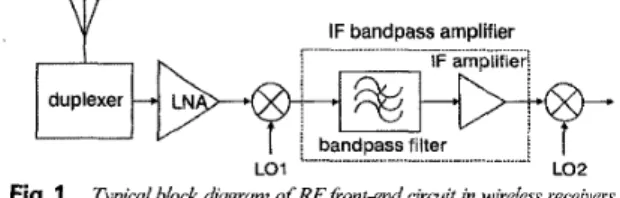
A typical block diagram of the RF front-end circuit in wireless receivers is shown in Fig. 1. The circuit consists of a duplexer, a low noise amplifier (LNA), an intermediate frequency bandpass filter (IF BPF), a series of cascaded IF amplifiers and two downconversion mixers with associated local oscillators (LO). In CMOS design, both I F BPF and IF amplifiers can be combined together to form the IF bandpass amplifier (BPA) so that the function of the filter, amplifier and AGC can be realised efficiently with low power and small chip areas.
IF bandpass amplifier I IF amplifier! Lol LO2 IF bandpass amplifier Lol LO2
Fig. 1 Typical block dhgrum of RFfront-endcircuit in wireless receivers
In conventional mobile communication systems, the sur- face acoustic wave (SAW) bandpass filters play a key role because of their flat passband, sharp stopband rejection and high reliability features in the predominant applica- tions of cellular telephones and radio paging. Generally, at very high frequencies (VHF), these SAW devices can be used as the IF filters for cellular telephones, whose frequen- cies vary from 45 MHz to more than 200 MHz. For pager 0 IEE, 2001
IEE Proceedings o n h e no. 20010570
DOL 10.1049/ipcds:20010570
Paper first received 18th April 2000 and in revised form 4th June 2001
Y. Cheng and J. Gong are with the Noise Laboratory, Department of Electri- calEngineering, National Tsing-Hua University, 101, Sec. 2, Kuang Fu Road, Hsinchq Taiwan 300, Republic of China
C.-Y. Wu is with the Integrated Circuits and Systems Laboratory, Institute of
ElectronicS and Department of Electronics Engineering, National chlao-Tung University, 1001 Ta Hsueh Road, Taiwan, Republic of China
applications, the SAW bandpass filters with narrow flat bandwidths are operated at frequencies 138-174MHz. However, one major problem with these passive SAW devices is that they generally have high insertion loss. Therefore, new design techniques for SAW filters have been proposed to reduce the insertion loss drastically and to meet the specifications of mobile communication sys- tems [l].
As well as the SAW filters, several single-chip pager receivers [2, 31 and a monolithc filter [4, 51 for applications in mobile communication systems have been implemented using the bipolar, silicon bipolar, GaAs and BiCMOS RFIC process technologies which are well suited to this market. In CMOS technology, there have been few impres- sive monolithic fdters proposed s o far, although much effort has been devoted to the research of
RF
components in CMOS technology.In recent years, most I F BPFs have been designed with transconductance-C (Gm-C) filters in CMOS technology [&lo]. The basic element in Gm-C filters is the integrator
formed by an open-loop transconductance element with a
capacitive load. So, the main difficulty in designing Gm-C filters for 6&200MHz IF applications is the high sensitivity to output parasitic capacitance and significant power dissi- pation. Moreover, many cascaded filter stages are required
to achieve the specified sideband rejection in R F receivers. Thus Gm-C filters are not suitable for the design of I F
BPAs for CMOS low-power RF receivers.
In t h s paper, a new circuit structure of a 2V CMOS IF BPA based on the Rm-C differentiator [l 11 is proposed and analysed. In this structure, a simple CMOS inverter-based Rm amplifier is connected with a capacitor to form an Rm-C biquad filter and a simple Q-enhancement circuit is incorporated to adjust the fdter operating frequency and gain. Thus filtering, amplifier and AGC functions can be realised in compact circuits. The proposed IF BPA has advantageous features of high sideband rejection, high gain and high linearity with the centre frequency around IO0 MHz.
2 Circuit structure
The basic element of the proposed Rm-C BPA is illustrated in Fig. 2 where the capacitor Cd is connected in series with the input of the Rm amplifer. It is called the Rm-C differ- entiator because the low-frequency transfer function
Vd
VIis equal to SCdR,. To realise the Rm amplifier for high- frequency applications, a simple NMOS inverter with shunt-shunt feedback resistance and current-source load is proposed [ll] as shown in Fig. 3. In Fig. 3, the PMOS transistor Mql biased by the gate voltage Ve is the current source as the inverter load. The feedback resistance is implemented by the NMOS transistor MNF biased by the gate voltage VcN in parallel with the PMOS transistor MPF
biased by the gate voltage Vcp. The crosscoupled PMOS transistors MpI and Mp2 are used to provide a negative resistance to the output node Vo. Thus the filter Q value can be increased. Since M p I is connected in parallel with
A4 the negative resistance can be adjusted by the gate voltage Ve of Mql. Generally, the smaller the Ve value, the larger the current of the inverter, and then the larger the magnitude of the gain.
Fig. 2 Basic element ofproposed Rm-CjZter
VDD
T
"CN 4_
By using small-signal analysis, the midband transresist- ance of the inverter-based R, amplifier can be expressed as
(1) 1
R
N-
(
)z;: g m i ( g d - g n )where g,, = g,,, is the transconductance of M,,, gf is the feedback conductance, g, is the magnitude of the negative resistance, and gd = gdnl
+
gdql is the total output conduct- ance which is the sum of output conductances gdnl and gdql of M,,, and Mql, respectively.In the shunt-shunt feedback resistance rf realised by MNF
and MpF, the source-drain voltage is zero and both MOS devices are operated in the triode region. By using the equation of drain current, the resistance rfcan be derived as I E E Proc -Circuits Devices Syst., Vol. 148, No. 6, December 2001
where
is satisfied by designing a suitable dimension ratio (W,,/L,,)/ ( WJLp). V,, ( Vt,) is the threshold voltage of the NMOS
(PMOS) device,
GP)
is the electron (hole) mobility,CO,
is the oxide capacitance per unit area and W, (Wp) and L,
(L,) are the channel width and channel length of the NMOS (PMOS) device. As seen from eqn. 2,
rf
is a volt- age-controlled resistor with a resistance value dependent on the control voltages VcN and Vcp Since the dependence ofVcN and Vcp on rf is linear in eqn. 2, the resistance tuning through VcN and Vcp can be performed easily.
"in ci
- 0
-
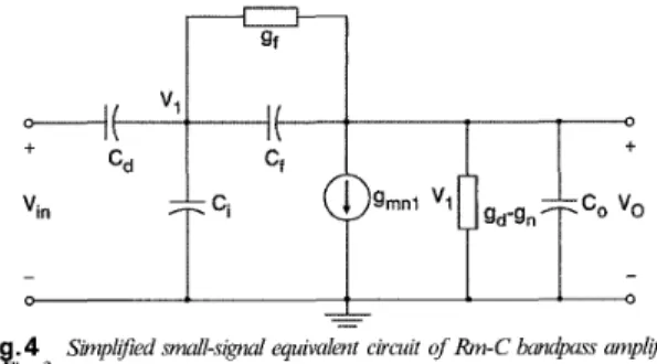
Fi .4 SimpifEd m l l - s i g d equivalent circuit of Rm-C bandpus umpliJ?er in!& 3
Considering the intrinsic capacitance of the MOS transis- tors as filter elements, the basic Rm-C differentiator in Fig. 3 can be regarded as a biquadratic BPF. The small- signal equivalent circuit of Fig. 3 is depicted in Fig. 4,
where CO is the total output capacitance including the capacitance of the MOS transistors and the external capac- itance loading C,, Ci is the input capacitance at the gate of
M n l , and
Cf
is the capacitance between the output node and the input node of M,,. The transfer function can be expressed as where A E ( c d+
C z ) ( C f+
C O )+
CfCo (4) (5) ( 6 ) (7) (8) (9)cf
E C g d n l (10) (11) E g m n lc
f + ( g d - g n ) (cd
-kcz
+
c f)
$9 f ( c d+
ct
+CO)
CE
(gmnl -k g d - g n ) g f D E -(gmn1 - g f )+
S C fcz
E C g s n l+
C g b n l f c g d n f+
C d b n f+
C g s p f -k C s b p fCO
E C d b n l x d b p l + c g s n f G g d p f + C s b p f + C d b p f + c L g d E g d n l+
g d p lFrom eqns. 7 and 10, it can be seen that Cf is very small so that SCf is much smaller than gmnl - gr. Thus SCf in
D
can be neglected. This means that D is a constant and H(S) in eqn. 3 can be approximated as the transfer function of abiquadratic bandpass filter.
According to eqn. 3 with constant
D,
the centre fre- quency w o and the quality factor Q of the VHF biquad can be expressed as Q = -m -
-J[~cd+c~~(c,+co)+c,c,]
( S m n l + S d - Sn)Sf B SmnlCf+
(Cd+
cz
+
C,) ( S d - gn)+
( C d+
cz
+
Co)g, (13) As mentioned before, gf is tunable by the voltages VcN andVcp, whereas g, is tunable by VQ. It can be seen from
eqns. 12 and 13 that the changes of gf and g, lead to the change of w, and Q. Although g, or VQ has a stronger effect on Q and gf or VcN ( Vcp) on w,, both Q and w o are
changed with g, and gf Thus iterative tuning is required to obtain the desired Q and
w,.
If process variationsare
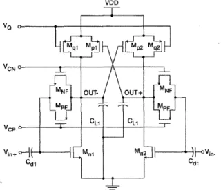
small from run to run, VcN ( Vcp) and VQ may be on-chip gener- ated and the resultant errors on Q and wo are still tolerable.With the basic circuit of Fig. 3, the fully differential IF Rm-C biquadratic bandpass amplifier (BPA) can be designed as shown in Fig. 5. It has a simple structure to retain high-frequency response. Moreover, the crosscoupled PMOS transistors can be compactly merged. They can provide the required negative resistance to both output nodes. Besides, they can also suppress the common-mode gain of the differential BPA to raise its common-mode rejection ratio (CMRR). VQ 'CN VCP "in+ VDD -T- I
Fig. 5 Circuit diagram of fully d@iential Rm-C IF biquadratic BPA
The required BPA for R F receiver applications is of about six orders. T h ~ s can be realised by directly cascading three stages of the biquadratic BPAs in Fig. 5 with VQ in the three stages connected together and similarly VcN and
Vcp Owing to the input capacitance C,, the
DC
voltage in one stage is blocked to the next stage. Thus, the problem ofthe DC voltage among stages can be avoided without
adding any extra element. 3 Stable conditions
Fig. 3 shows the implementation of negative resistance directly using a positive feedback circuit which is composed of two identical PMOS transistors crosscoupled to each
other. The purpose of these extra positive feedback circuits is to generate a higher gain value. The positive feedback circuit willcreate a negative conductance
where gmp is the transconductance of Mp and gdp is the load conductance seen from the load terminal. The total output conductance g, is now the parallel combination of go and
g,, i.e. g, = go - g,. By designing the relative sizes such that
the negative conductance will cancel most of the positive conductance at the output stage, a higher impedance and consequently hgh Q can be achieved.
If g, is negative, the Q-factor and the gain of the BPF increase. However, the g, value cannot be too negative. The potential problem associated with the use of positive feed- back is the tendency for oscillation to occur in the circuit. It is obvious that the fully differential biquadratic Rm-C BPF has two poles and they are negative real numbers or conju- gate complex numbers in the left-half plane if the circuit system
is
stable. Thus, the coefficientsB > 0
and C> 0
in eqns. 5 and 6. That isAlthough the g, value cannot be precisely quantified, eqn. 14 gives the range that has stable operation for the Rm-C BPF circuit.
4 Measured results
The proposed Rm-C IF BPA has been designed and simu-
lated with 0.5 pm double-poly-double-metal CMOS tech-
nology. After the design optimisation, component values
and device dimensions of the 100MHz CMOS bandpass
amplifier are listed in Table 1. All MOS devices have the minimum gate length of 0 . 5 ~ to reduce the device capaci- tance. The active chip area is about 635 x 9 6 0 ~ ~ . Table 1: Component values and device dimensions of IF fil- ter
1st stage 2nd stage 3rd stage W L , & N L ' M w L , M Device Pm Pm Pm Pm Pn Pm PMOS (mpl, mp2) 5 0.5 30 5 0.5 30 5 0.5 20 PMOS (mql,mq2) 5 0.5 40 5 0.5 20 5 0.5 30 NMOS(mn1,mnZ) 20 0.5 50 20 0.5 50 20 0.5 40 PMOS (mspl) 5 0.5 40 5 1 40 5 1 50 NMOS(msn1) 2 0.5 40 2 0.5 40 2 0.5 50 cdl I cd2 2 PF 2 PF 1 PF CLI, cL2 5 PF 5 PF 5 PF
Fig. 6 shows the measured frequency response of the three-cascaded-stage high-gain Rm-C IF bandpass ampli- fier with Vcp = O.lV, VcN = 1 .68V and VQ = 0.51V and the supply voltage V,, = 2V. The differential-mode gain is 20 dB whereas the common-mode gain is -25 dB so that the
CMRR is 45dB. Normally the IF BPA has to be large in
order to be able to perform the high-frequency mirror signal suppression with a bandpass filter with limited Q. It has out-of-band signal suppression comparable to the ideal sixth-order BPF. If the frequency of the desired signal is IEE Proc.-Circuits Devices Syst., Vol. 148, No. 6, December 2001 320
80 MHz and the frequency of the mirror signal is 120 MHz, an equivalent mirror signal suppression of 20dB can be obtained by the proposed I F BPA.
20 0 m P U .- g-20 -40 -60 1 06 1 o7 1 08 frequency, Hz Fig.6
BPA Mearuredfiequmcy response offully d'fferential6th-orakr Rm-C IF
VDD = 2V, VCN = 1.68V, Vcp = O.IV, Ve 2 0.57V
*O
r
/I-60 -40 -20
Pin, dBm
M e w e d IidB, O P , , UP3, and OIP3 of fully diwentiul6th-order Fig. 7 P"l 0 P"2 Rm-C IF BPA - line 1 line 2 _ _ _
The measured input and output 1 dB compression points IPlds and 0PldB and input thrd-order intercept point IIP3 are -21 dBm, 4 d B m , and -5dBm, respectively, as shown in Fig. 7. The dynamic range DR = (IPldB - MDS) = 50dB, since the minimum discernible signal (MDS) is
4 5 d B m . The bandwidth of the IF BPA is about 40MHz.
The chip power consumption is 14mW under a 2V power Fig. 8 shows the measured tunability of the fully differ- ential sixth-order IF BPA with fixed VcP = 0.1 V and VcN
= 1.75V, and variable VQ from 0.26 to 0.94V. As can be seen from Fig. 8, the adjustable gain of the I F BPA is in the region of 55dB with only a small change of centre frequency. Thus, the control voltage VQ may be used to perform the automatic gain control (AGC). In the tuning of the IF BPA, the initial values of the controlled voltages are VcP = O.lV, VcN = 1.75V, and VQ = 0.57V. After finding the optimal values, one of the controlled voltages can be kept constant while the other is adjusted to perform the fine tune. As shown in Fig. 9, the measured centre frequency of the BPA varies from 41 to 178MHz whereas there is no gain variation in the passband. Under the condi- tion of VcP = O.lV, VcN = 1.61
-
1.95V and VQ = 0.26-
supply.IEE Proc.-Circuits Devices Syst., Vol. 14& No. 6, December 2001
0.94V, the tunability of the centre frequency is 137MHz. The measured results of the fully differential sixth-order Rm-C BPA are summarised in Table 2. The layout of the IF BPA is shown in Fig. 10.
20 - 0 - % ai m
2
-20 9 * Q f -40 -60 .nn "" 1 06 1 07 108 1 09 frequency, Hz Fig. 8 BPA Vcp = 1 V, VcN = 1.75V, Ve = 0.26Q.94V Ve values: 0.74v ~ 0.26VMeasured frequency responses of fully dgerentiul 6th-orakr Rm-C
_ _ _ 0.83V 0 94v _ _ 0 40V 0 52v 0 63V _ _ _ _ _ _ _ _ _ _ _ -40 .fin " _ 1 08 1 09 IO7 frequency, Hz 1 06 Fig.9
BPA Measuredfreguency responses of fully differential 6th-orAer Rm-C
v,, = 2.0v, vp = l S V , vcp = 0.1v
~ VCN = 1.61V V = 0.87V
. . . VcN = 1.74V'
4
= 0.4V _ _ _ _ Vav = 1.95V:6
= 0.OVFig. 10 Photograph of IFBPA chip
5 Conclusions
A new CMOS 2V low-power fully differential Rm-C band- pass amplifier (BPA) with low power dissipation suitable for application in the IF stage of R F receivers has been successfully designed, analysed and fabricated by using
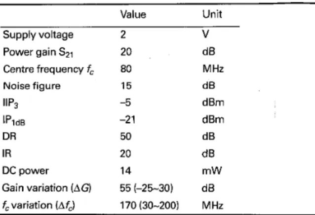
Table 2: Measured results of IF BPA Value Unit Supply voltage 2 V Power gain Spl 20 dB Centre frequency fc 80 MHz Noise figure 15 d 0 IIP3 -5 dBm lPldB -2 1 dBm DR 50 dB IR 20 dB DC power 14 mW
Gain variation (AG) 55 (-25-30) dB
fc variation (Aft) 170 (30-200) MHz
0.5 pn double-poly4ouble-metal CMOS technology. In this design, the voltage mode bandpass biquads are imple- mented by the transresistance amplifier-capacitor (Rm-C) structure. The tunable shunt-shunt feedback MOS resistor
and a crosscoupled PMOS load are applied to the biquad-
ratic fdter. Thus, both centre frequency and gain of the IF BPA are fully adjustable to account for processing toler- ances and drifts caused by temperature variation or chang- ing operating conditions. The performance of the proposed Rm-C BPA has been verified through measured results on a sixth-order BPA design. Besides the above, the proposed biquad is suitable for low-power and low-voltage applica- tions. Suitable central frequency, amplifier gain and low- power dissipation make the proposed bandpass amplifier quite feasible in the IF stage for wireless communication applications.
6 Acknowledgments
The authors would like to thank the Chip Implementation Center (CIC) of the National Science Council (NSC), Taiwan, ROC and United Microelectronics Corporation (UMC) for their kind valuable advice and support to implement the chip.
7 References
1 MACHUI, J., MULLER, G., RUILE, W., REINDL, L., WEIGEL, R., and RUSSER, P.: ‘A new low loss SAW filter structure with extremely wide bandwidth for mobile communication systems’,
IEEE MTT-S Int. Microw. Symp. Dig., 1993, pp. 1501-1504 2 CASTELLO, R., BIETTI, I., and SVELTO, F.: ‘High-frequency
analog filters in deep-submicron CMOS technology’. ISSCC Dig. Tech. Papers, February 1999, pp. 74-75
3 VANCE, I.A.W.: ‘Fully integrated radio paging receiver’, ZEE Proc. F, 1982, 129, (I), pp. 2 4
4 SAUL, P.H.: ‘Design techniques for VHF and UHF monolithic Si-
con filters’. Proceedings of IEE Colloquium on Digital and analogue
filters and filtering systems, 1990, pp. 711-714
5 NGARMNIL, J., and TOUMAZOU, C.: ‘New approach for high order-high frequency analogue micropower filter design’. Proceedings of 1997 IEEE Intemational Symposium on Circuits and Systems, June 1997, pp. 8 H 8
6 WANG, Y.T., and ABIDI, A.A.: ‘CMOS active filter design at very high frequencies’, IEEE J. Solid-State Circuits, 1990, 25, pp. 1562- 1574
KHOURY, J.: ‘Design of a 15-MHz CMOS continuous-time fdter with onchip tuning’, IEEE J. Solid-state Circuits, 1991, 26, pp. 1988-
1997
8 NAUTA, B.: ‘A CMOS transconductance-C filter technique for very high frequency’, IEEE J. Solid-State Circuits, 1992, 27, pp. 142-153 9 SNELGROVE, W.M., and SHOVAL,A.: ‘A balanced 0.9 pm
CMOS transconductance-C filter tunable over the VHF range’, IEEE
J. Solid-State Circuits, 1992, 27, pp. 314323
IO ANON, : ‘High-frequency filter demand increasing’, JEE, 1988, pp.
72-74
11 LU, P.H., WU, C.Y., and TSAI, M.K.: ‘Design techniques for VHF/ UHF high Q tunable bandpass filters using simple CMOS inverter- based transresistance amplifiers’, IEEE J. Solid-Stute Circuits, 1996,
31, pp. 719-725 7