J. Electrochem. Soc., Vol. 142, No. 10, October 1995 9 The Electrochemical
Society, Inc. L187Acknowledgment
This study is supported by the Engineering and Physical Science Research Council, United Kingdom.
Manuscript submitted March 27, 1995; revised manuscript re- ceveid July 10, 1995.
The University of Essex assisted in meeting the publication costs of this article.
REFERENCES
1. C. M. Seymour, J. Power Sources, 37, 155 (1992).
2. L.W. Niedrach and I. B. Weinstock, Electrochem. Technol., 3, 270 (1965).
3. L. W. Niedrach, D. W. McKee, J. Paynter, and I. F. Danzig, ibid., 5, 318 (1967).
4. G.A. Hards, T. R. Ralph, and S. J. Cooper, ETSU Report, No. ETSU/FCR/002, Dec. 1992.
5. A. C. C. Tseung, P. K. Shen, and J. Syed-Bokhari, PCT Int. Appl. WO92 16,027, Sept. 17, 1992; GB Appl. 91/4,377,
March 1, 1991.
6. P. K. Shen and A. C. C. Tseung, This Journal, 141, 3082 (1994).
7. P. K. Shen, K. Y. Chen, and A. C. C. Tseung, J. Chem. Soc., Faraday Trans.,
90,
3089 (1994).8. K. Y. Chen, P. K. Shen, andA. C. C.Tseung, This Journal, 142, L54 (1995).
9. P. K. Shen, K. Y. Chen, and A. C. C. Tseung, J. ElectroanaL Chem., In press.
10. P. K. Shen, K. Y. Chen, and A. C. C. Tseung, This Journal, 142, L85 (1995).
11. A. C. C. Tseung and L. Wong, J. AppL Electrochem., 3, 211 (1972).
12. B. S. Hobbs and A. C. C. Tseung, This Joumal, 119, 580 (1972).
13. S. Gottesfeld and J. Pafford, ibid., 135, 2651 (1988). 14. J. C. Amphlett, K. A. M. Creber, J. M. Davis, R. F. Mann, B. A.
Peppley, and D. M. Stockes, Proc. 9th World Hydrogen En- ergy ConL, Paris, France, June 22-25, 1992, p.1541. 15. S. H. Oh and R. M. Sinkevitch, J. CataL, 142, 254 (1993).
A Novel Planarization of Trench Isolation Using
Polysilicon Refill and Etchback of
Chemical-Mechanical Polish
Juing-Yi Cheng, a Tan Fu Lei, a Tien Sheng Chao *'b
~Department of Electronics Engineering and Institute of Electronics, National Chiao Tung University and bNational Nano Device Laboratory, Hsinchu, Taiwan
ABSTRACT
The planarization of trench isolation refilled by deposition of polysilicon was investigated. Results show that the planarization by RIE etching has poor surface planarity. On the other hand, an excellent surface planarity can be achieved by the CMP process resulting from the high etching selectivity of polysilicon to nitride. This simple process provides a very promising candidate for trench isolation.
Introduction
As device geometries are scaled down to the deep submicron regime, processes of integrated circuits become more and more complex and multilevel interconnection is used to achieve high- speed performance. Hence, the planarization of silicon surface be- comes a key processing step. The surface topography of integrated circuits is easier to planarize if the silicon wafer is planarized from the initial isolation process.
In a deep-trench isolation structure, the polysilicon is typically used as trench refill material. The technique of planarization based on the reactive-ion-etching (RIE) process of polysilicon trench refills has been widely utilized. 1'2 However, conventional RIE processes show problems with nonuniform plasma etching. Furthermore, voids and damaged regions are generated due to the preferential plasma etching along polysilicon grain boundaries. 3'4 Because of dints at the center of the deep trenches; the planarization process of RIE etchback still results in a poor surface planarity.
In order to overcome these problems mentioned above, a satisfy- ing technology for etch and planarizing the polysilicon refilled trench is required. The planarization of oxide-filled trenches based on a chemical-mechanical polishing (CMP) process has been pro- posed to achieve an excellent surface planarity. ~'6 However, it is difficult to control, and the planarity always gets worse because there is no stopper for oxide etchback. 6 This paper presents a novel planarization technique using polysilicon refill and a well-operated CMP process to circumvent these problems.
Experimental
In order to evaluate the removal rate of polysilicon film, a 600 nm thick polysilicon layer was deposited by low pressure chemical vapor deposition (LPCVD) at 620~ on a 100 nm thick silicon diox- ide layer which was grown on the p-type (100) silicon wafers by wet
* Electrochemica) Society Active Member.
oxidation at 980~ For silicon nitride rate determination, a 200 nm thick LPCVD silicon nitride (SIN) layer was directly deposited on p-type (100) silicon wafers at 780~ The polishing slurry used in this experiment is colloidal silica in an aqueous KOH solution with PH~I 1.0 (RODEL 2371). The viscosity of slurry is smaller than 25 cps. The silica particles are uniform in size and the mean particle diameter is 80 nm. The polishing pad is a microporous polyurethane material and the hardness of pad is 52~62 Shore D. As the wafer undergoes polishing (Westech Model 372M wafer polisher), the film on the substrate will be removed. The flow rate of slurry was 200 ml/min and the platen temperature was set at 98~ during polish.
Test structures of the deep trench were fabricated on p-type (100) silicon wa)'ers. According to Fig. 1, the trench hard mask was first fabricated consisting of 30 nm thermally grown pad oxide and 120 nm SiN. The trench hard mask was etched first by R IE and then silicon trench was performed by a CI2/O2/SF6 plasma. After the removal of photoresist, the wafers were cleaned. A 20 nm thick screen oxide was thermally grown in an 02 ambient and stripped in a buffer HF solution to remove damage. After the screen oxide was stripped, 35 nm thick silicon dioxide was grown again in an 02 ambient at 925~ Then, 900 nm thick LPCVD polysilicon was deposited to refill the deep trench.
Results and Discussion
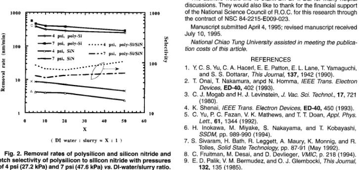
The removal rates of polysilicon and SiN with pressures of 4 psi (27.2 kPa) and 7 psi (47.6 kPa) vs. the water/slurry ratio are shown in Fig. 2. The removal rate of polysilicen reaches 405 nm/min at 4 psi (27.2 kPa) and 560 nm/min at 7 psi (47.6 kPa) with a dilute 3:1 slurry. The removal rate of SiN is only 4.4 nm/min at 4 psi (27.2 kPa) and 8.75 nm/min at 7 psi (47.6 kPa) with the same slurry. Hence, higher pressure results in higher removal rate. 7 The reason for the significantly higher removal rate of polysilicon is that the strength of the Si--Si bond is weaker than that of the Si--N bond. Within the
) unless CC License in place (see abstract).
ecsdl.org/site/terms_use
address. Redistribution subject to ECS terms of use (see
140.113.38.11
L188 J. Electrochem. Soc., Vol. 142, No. 10, October 1995 9 The Electrochemical Society, Inc.
Fig. 1. Deep-trench isolation structure of polysilicon refill.
polishing process, the temperature is elevated due to the friction of the slurry particle, pad and wafer surface. 8 Therefore, the chemical- removal rate of polysilicon becomes a critical component of the removal process. 7-9 The chemical reactions taking place in water separating silica surface molecules from the bulk are progressively asT, 8
~--Si-- + 4 OH- ---> ~ S i - - O H + 3 OH- ---> =Si(OH)2
+ 2 OH- ~ -Si(OH)3 + OH --> Si(OH)4 However, the chemical-removal rate of SiN has little influence on the removal process.
The etch selectivity of polysilicon with respect to SiN also shown in Fig. 2 is very high. The etch selectivity of polysilicon to SiN reaches 92 at 4 psi (27.2 kPa) with a dilute 3:1 slurry. Lower pres- sure results in higher selectivity.
The complete structure of polysilicon trench refill is shown in Fig. 1. There is a dint in the center of the deep trench. The etchback of polysilicon trench refill in a CIJ02 plasma enhances the dint at the center of the deep trench as Fig. 3(a), while the etchback and planarization of polysilicon trench refill based on a CMP process as Fig. 3(b) has excellent surface planarity at 4 psi (27.2 kPa) with a dilute 3:1 slurry.
Conclusion
Two planarization approaches of polysilicon trench refill have been evaluated. The RIE process results in poor surface planarity. On the other hand, an excellent planarization has been demon- strated successfully based on a well-operated CMP process. High etch selectivity of polysilicon to SiN can be achieved in a dilute KOH slurry. Selectivity is pressure-dependent. This simlple process of
1 0 0 0 ! . . . . , . . . . , . . . . i . . . . , . . . . , . . . . , 1 0 0 0 4 p s i , p o l y - S i 9 7 p s i , p o l y - S i . . . 4 p s i , p o l y - S i / S i N ~ , ' ~ - - 4 p s i , S i N ~ - o 7 p s i , p o l y - S i / S i N 7 p s i , S i N
~
- ~ 1 7 6 1 7 6 E l o o 1 1 0 0 1 0 2 0 3 0 4 0 5 0 6 0 1 0 0 w -e ( D I w a t e r : s l u r r y = X : 1 )Fig. 2. Removal rates of polysilicon and silicon nitride and etch selectivity of polysilicon to silicon nitride with pressures of 4 psi (27,2 kPa) and 7 psi (47.6 kPa) v s . DI-water/slurry ratio,
Fig. 3. SEM cross-sectional view: (a) the etchback of polysil- icon trench refill in a Ci2/O2 plasma ambient and (b) the etch- back and planarization of polysilicon trench refill based on a CMP process.
polysilicon refill and CMP is a very promising candidate for trench isolation.
Acknowledgment
The authors would like to thank Dr. B. T. Dai for many helpful discussions. They would also like to thank for the financial support of the National Science Council of R.O.C. for this research through the contract of NSC 84-2215-E009-023.
Manuscript submitted April 4, 1995; revised manuscript received July 10, 1995.
National Chiao Tung University assisted in meeting the publica- tion costs of this article.
REFERENCES
1. Y. C. S. Yu, C. A. Hacerl, E. E. Patton, E. L. Lane, T Yamaguchi, and S. S. Dottarar, This Journal, 137, 1942 (1990). 2. T. Onai, T. Nakamura, anpd N. Homma, IEEE Trans. Electron
Devices, ED40, 402 (1993).
3. C. J. Mogab and H. J. Levinstein, J. Vac. Sci. TechnoL, 17, 721 (1980).
4. K. Shenai, IEEE Trans. Electron Devices, ED-4O, 450 (1993). 5. C. Yu, P. C. Fazan, V. K. Mathews, and T. T Doan, Appl. Phys.
Lett., 61, 1344 (1992).
6. H. Inokawa, M. Miyake, S. Nakayama, and T. Kobayashi, SSDM, pp. 989-990 (1994).
7. S. Sivaram, H. Bath, R. Leggett, A. Maury, K. Monnig, and R. Tolles, Solid State Technology, pp. 87-91 (May 1992). 8. C. Fruitman, M. Desai, and D. Devlieger, VMIC, p. 218 (1994). 9. E. D. Palik; V. M Bermudez, and O. J. Glembocki, This Joumal,
132, 135 (1985).
) unless CC License in place (see abstract).
ecsdl.org/site/terms_use
address. Redistribution subject to ECS terms of use (see
140.113.38.11