國 立 交 通 大 學
光 電 工 程 研 究 所
碩士論文
利用無色散間隔器
探討雙向光纖傳輸系統
Study of bidirectional transmission system
using novel four-port interleavers
研
究
生 : 林 擇 雨
指 導 教 授
: 祁 甡 老師
: 陳 智 弘 老師
利用無色散間隔器
探討雙向光纖傳輸系統
Study of bidirectional transmission system
using novel four-port interleavers
研 究 生 :林擇雨
Student :
Tse-Yu
Lin
指導教授
:陳智弘 老師
:祁 甡 老師
Advisor
: Assistant Prof. Jyehong Chen
: Emeritus Prof. Sien Chi
國 立 交 通 大 學
光 電 工 程 研 究 所
碩 士 論 文
A Thesis
Submitted to Institute of Electro-Optical Engineering
College of Electrical Engineering and Computer Science
National Chiao Tung University
In Partial Fulfillment of the Requirements
For the Degree of Master In
Department of Photonics
July 2006
Hsinchu, Taiwan, Republic of China
致謝
A
CKNOWLEDGEMENT 完成這篇論文,我由衷感謝師長的指導與學長、同學們的鼎力相助。回顧這 兩年來攻讀碩士,過程中的飛鴻麟爪、點點滴滴,不僅充實我在學識方面的視野, 也習得了待人處事的涵養。在此,我特別感謝一路上提攜我的良師益友: 謝謝祁 甡老師提供我自由研究的機會,不論是研究所初期在工研院實習或是後來回到光 纖通訊實驗室做實驗; 感謝陳智弘老師指導我光電研究,陳老師提供一個有效率 且和樂融融的研究環境,也鼓勵大家在研究之餘多作運動 – 因為擁有強健的體 魄是做研究的基礎; 明芳學姐在我做實驗時大力相助,也耐心的聽我分析複雜的 模擬系統並與我討論模擬結果; 嘉建學長在我對理論感到困惑或是模擬遇到瓶頸 時,總是能深入淺出的點出解決之道; 一同共事的重佑學長,教導我做實驗的技 巧與要點。除此之外,也要謝謝同實驗室伙伴,昱璋學長、炫涵學長、蔡昇祐同 學、周森益學長、五樓光纖通訊實驗室的學長同學們及六樓工研院光通訊實驗室 的學長們,對我的包容,為大家寧靜的研究生生活帶來些許噪音。還有,謝謝柏 元同學,從推甄研究所到碩士班畢業,一直以來的扶持和鼓勵。最後,我要感謝 我的爸爸、媽媽,由於他們從小到大的栽培,而且始終對我有信心,得以讓我無 後顧之憂的在求學路上奮鬥。總歸來說,因為有這麼多人的相助,點點滴滴的累 積,才有今日的我。 擇雨 2006/07/21利用無色散間隔器
探討雙向光纖傳輸系統
學生:林擇雨 指導教授 : 祁 甡 教授
陳智弘 教授
國立交通大學光電工程研究所碩士班
摘要
在一個光纖鏈結中執行雙向傳輸為一吸引人的架構。雙向傳輸不僅可減少一 半的基礎設施—例如傳輸光纖,光學分光器和光纖放大器—, 還可增加頻寬的使 用率。然而,要實現雙向放大和阻絕雷利後散射是雙向傳輸系統中所需要克服的 困難。因此我們提出了利用間隔器組成一個單向放大路徑的結構用以達成雙向傳 輸的效果。 在本論文中,先研究間隔器的相關原理和數學模型的建立,並且附上實際元 件量測與間隔器在單向放大路徑的結構之操作。我們架設了兩個雙向傳輸系統 (直接雙向傳輸架構與雙向迴路架構),實驗測試以間隔器為基礎的雙向放大器的 可行性。且由這兩個實驗的結果所啟發,我們利用 VPI 這一模擬軟體模擬比較直 接雙向傳輸架構與雙向迴路架構。總的說來,由實驗結果和模擬結果展露出一項 訊息: 若使用雙向迴路架構評估長距離雙向傳輸系統,將會獲得一過於樂觀的系 統效能評估。Study of bidirectional transmission system
using novel four-port interleavers
Student:Tse-Yu Lin Advisor : Dr. Sien Chi
Dr. Jyehong Chen
Institute of Electro-Optical Engineering
National Chiao Tung University
Abstract
Bidirectional transmission over a single fiber link is an appealing architecture. Not only could it reduce the infrastructure -- such as fibers, optical splitters and optical amplifiers -- by a factor two, but it also increases the potential of bandwidth utilization. However, realization of bidirectional amplification and Rayleigh backscattering are the difficulties among bidirectional transmission. Therefore, we proposed a unidirectional amplification scheme which facilitates bidirectional transmission by using an interleaver.
In this thesis, the principle and mathematical model of the interleaver are studied first, where the experimental measurement and operations of an interleaver are included as well. In a bidirectional transmission system, we installed two bidirectional transmission systems (i.e., straight line and re-circulating loop configurations) to demonstrate the feasibility of such interleaver-based bidirectional amplifier. Afterward, inspired by the experimental results, we simulated both the loop and the straight line bidirectional transmission systems. All in all, both experimental and simulation results reveal that it is over-optimistic to estimate long distance bi-directional transmission performance using a re-circulating loop.
C
ONTENTSAcknowledgement
... iChinese Abstract
... iiEnglish Abstract
... iiiContents
... ivList of Figures
... viList of Tables
... xCHAPTER 1 Introduction
1.1 Bi-directional transmission system...11.2 Motivation of research...2
1.3 Structure of this thesis...3
CHAPTER 2 Characteristics of interleaver
2.1 Introduction...52.2 Digital Concepts for Optical Filters...5
2.2.1 Discrete Signals and Z-transform...6
2.2.2 Poles and Zeros...8
2.2.3 Magnitude Response and Group Delay...9
2.3 Interleaver...12
2.3.1 Interleaver technology approaches...12
2.3.2 Lattice Interleaver...12
2.3.3 Mathematical Derivation...16
2.3.4 Interleaver Simulation Results & Practical Device Measurement...17
CHAPTER 3 Experiment of bi-directional straight line
transmission
3.1 Bidirectional Optical Amplifier Configurations...25
3.2 Nonlinear effects...27
3.2.1 Stimulated Brillouin scattering...27
3.2.2 Rayleigh backscattering...29
3.3 Experimental setup & results of bidirectional straight line transmission...31
CHAPTER 4 Experiment of bi-directional loop transmission
4.1 Re-circulating loop transmission...384.1.1 Loop time control...39
4.1.2 Dispersion management...41
4.2 Experimental Setup & results of bidirectional loop transmission...43
CHAPTER 5 Simulation of bidirectional transmission systems
5.1.1 Analysis of bidirectional loop transmission system...485.1.2 Analysis of bidirectional straight transmission system...51
5.2 Simulation setup...52
5.2.1 Simulation setup of bidirectional loop system...54
5.2.2 Simulation setup of bidirectional straight system...56
5.3 Simulation results of bidirectional transmission...58
5.3.1 Case I: Bidirectional loop system...58
5.3.2 Case II: Bidirectional straight line system...61
5.3.3 Comparison of the “Loop” and “Straight Line” cases...64
5.4 Simulation of modified straight line transmission...66
5.5 Discussion...70
CHAPTER 6 Conclusions
REFERENCE
...74L
IST OFF
IGURESFig. 2.1 Illustrations of single-stage (a) MA digital filter and (b) AR digital filter. Fig. 2.2 Pole-zero diagram showing the unit circle, one pole, and one zero. Fig. 2.3 Pole-zero diagram showing a maximum- and a minimum-phase zero. Fig. 2.4 Phase response of maximum and minimum phase MA filers.
Fig. 2.5 Brief configuration of an L-2L interleaver Fig. 2.6 The periodic rectangular function
Fig. 2.8 Transmission responses of the even and odd channels.
Fig. 2.9 The bandwidth estimations of -0.1dB and -0.5dB for L-2L interleaver. Fig. 2.10 Detail configuration of an L-2L interleaver
Fig. 2.11. Measured amplitude response of the interleaver for even and odd channels Fig. 2.12(a). Amplitude response and the corresponding group delay of the interleaver for odd channels (type II)
Fig. 2.12(b). Amplitude response and the corresponding group delay of the interleaver for even channels (type I)
Fig. 2.13. Passband of the interleaver for even and odd channel Fig. 2.14. Transmission of Interleaver
Fig. 2.15. Wavelength re-routing scheme for bidirectional transmission
Fig. 2.16 (a) In-band group delay for two types of interleaver, (b) group delay of cascading Type I and Type II.
Fig. 3.1 (a) Bidirectional amplification with unidirectional optical amplifier (b) Bidirectional amplifier with optical isolation (c) double optical amplifier with shared pump laser.
Fig. 3.2. Scheme of crosstalk due to single- and double-amplified RB of signal as well as ASE. PASE is the power of ASE noise from the EDFA. Esd is the downstream signal, and Es
u
is the upstream signal. ERB and E are the Rayleigh backscattered
d
RB u
signals of Esd and Esu , respectively.
Fig. 3.3. Experimental setup of a bidirectional transmission
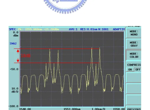
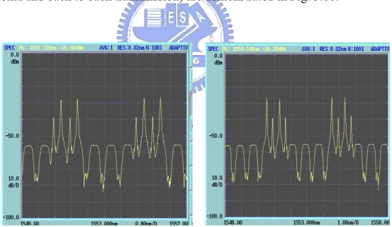
Fig. 3.4(a).Received optical spectrum of the east-even traffic after 160-km transmission
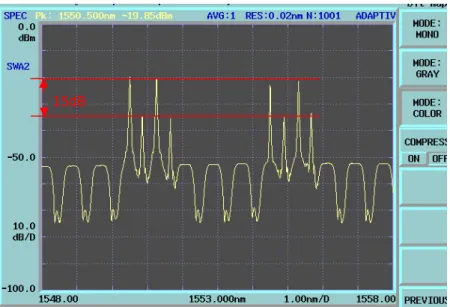
Fig. 3.4(b).Received optical spectrum of the west-odd traffic after 160-km transmission
Fig. 3.5. Primary reflection path
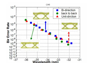
Fig. 3.6. BER curves and corresponding Eye diagrams after 210-km transmssion @ CH. 6
Fig. 3.7. Power penalty of each channel
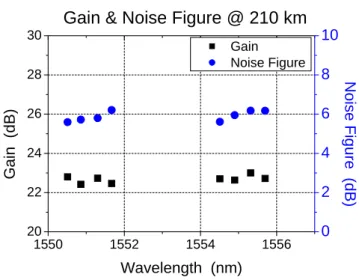
Fig. 3.8. Noise figure and net gain of the proposed bidirectional amplifier Fig. 3.9. Optical spectrum before the receiver
Fig. 3.10. BER curves and corresponding Eye diagrams after 210-km transmission @ CH. 6
Fig. 3.11. Power penalty of each channel for 210km transmission
Fig. 3.12. Net gain and noise figure of each channel for 210km transmission Fig. 4.1. loop transmission block diagram
Fig. 4.2. (a) load state (b)loop state
Fig. 4.3. pulse signaling for loop time control
Fig. 4.4. Dispersion map (fully compensated @ 1553.2 nm, Max △D in CH 1 equals to 95.5 ps/nm)
Fig. 4.5. Experimental setup of bi-directional loop transmission
Fig. 4.6. Received optical spectrum after 500 km bidirectional transmission Fig. 4.7. Power penalty after 500 km bidirectional loop transmission
Fig. 4.8. BER curves of Channel seven after 0 km, 100 km, 300 km, 500 km traffic Fig. 4.9(a)~(d). Corresponding eye diagrams of Channel 7 after 0 km, 100 km, 300
km, 500 km
Fig. 4.10. Accumulated Errors after 100 km and 500 km bidirectional transmission at BER = 2.46 × 10⁻⁹
Fig. 5.1(a) Uni-directional loop and corresponding round trip analysis (b) loop time control
Figure5.2. (a) Configuration of original bidirectional loop (b) Loop time control of original bidirectional loop
Fig. 5.3(a) adjusted bidirectional loop configuration (b) loop time control Fig. 5.4 Bidirectional Loop System
Fig. 5.5 Bidirectional Straight Line System Fig. 5.6 Dispersion map used in simulation Fig. 5.7 Decomposed bidirectional loop system
Fig. 5.8 Decomposed bidirectional straight line system Fig. 5.9 Simulated bidirectional straight line system
Fig. 5.10. Received optical spectrum after 800 km bidirectional loop transmission Fig. 5.11 BER curves @ ch.10 after 0, 200, 400, 600 and 800-km bidirectional loop transmission
Fig. 5.12. Power penalty distribution of bidirectional loop transmission
Fig. 5.13 (a)~(f) Correspond eye diagrams after 0 km, 100 km, 200 km, 400 km, 600 km and 800 km bidirectional loop transmission
Fig. 5.14. Received optical spectrum after 800 km bidirectional transmission (straight line)
Fig. 5.15 BER curves @ ch.10 after 0, 200, 400, 600 and 800-km bidirectional transmission (straight line)
Fig. 5.16 Power penalty distribution of bidirectional transmission (straight line) Fig. 5.17. (a)~(f) Correspond eye diagrams after 0 km, 100 km, 200 km, 400 km,
600 km and 800 km bidirectional transmission (straight line)
Fig. 5.18 BER curves and corresponding eye diagrams @ ch.10 for “Loop” and “Straight Line” cases after 0 km and 800 km bidirectional transmission.
Fig. 5.19. Penalty distribution for “Loop” and “Straight Line” cases. Fig. 5.20 Modified Bidirectional Straight Line System
Fig. 5.21. Received optical spectrum after 800 km bidirectional transmission (modified straight line)
Fig. 5.22 BER curves @ ch.10 after 0, 200, 400, 600 and 800-km bidirectional transmission (modified straight line)
Fig. 5.23 Power penalty distribution of bidirectional transmission (modified straight line)
Fig. 5.24. (a)~(f) Correspond eye diagrams after 0 km, 100 km, 200 km, 400 km, 600 km and 800 km bidirectional transmission (modified straight line)
Fig. 5.25 BER curves and corresponding eyes @ ch.10 for case “Loop”, “Straight Line” and “Modified Straight Line”
Fig. 5.26 Penalty distribution for case “Loop”, “Straight Line” and “Modified Straight Line”
L
IST OFT
ABLESTable 1. Parameters of dispersion map for bidirectional loop experiment Table 2. Power penalty of bidirectional transmission experiments Table 3. Parameters used in bidirectional loop architecture. Table 4. Parameters used in bidirectional straight line architecture. Table 5. Simulation and experimental results
Chapter 1
Introduction
1.1 Bi-directional transmission system
In future communication network, besides dense wavelength-division- multiplexing (DWDM) scheme, bidirectional transmission over a single fiber link is also an appealing architecture. The main motivation for considering bidirectional transmission over a single optical fiber instead of “two-times unidirectional” is the reduction of the infrastructure (fibers, optical splitters and optical amplifiers) by a factor two and the potential of bandwidth utilization. As economical aspect, bidirectional wavelength-division-multiplexing (WDM) transmission system is an attractive scheme. Not only could it avoid building another new construction of fiber link, but also reduce the number of passive and active components, such as splitters and EDFAs, concurrently. Moreover, transmitting bi-directionally over a single fiber link can increase the capacity of twice as an installed unidirectional link. [1].
Rayleigh backscattering is one of the fundamental mechanisms in optical fiber that may cause crosstalk by the reverse channel [2]. It can be considered as an unavoidable background reflection level. In bidirectional networks employing optical amplifiers, signals are bi-directionally transmitted over a single fiber path. If optical isolators are not used to prevent multiple reflections, Rayleigh backscattering (or many small reflections) can significantly degrade the receiver sensitivity. Therefore, system performances are severely deteriorated on account of multiple reflections. It has been observed that due to multiple reflections along a fiber path, the laser phase noise is converted to intensity noise, which may cause performance degradation in high speed lightwave system. Even if discrete reflections are carefully suppressed by using non-reflective connector facets, the multi Rayleigh backscattering (RB) in fibers give rise to the phase-to-intensity noise conversion. Moreover, the interferometric noise from multiple RB increases proportionally with the optical amplifier gain. Thus, the
maximum gain of inline optical amplifiers without optical isolator is limited to 19 dB [3] because the additive intensity noise induced by RB.
Brillouin scattering is another fundamental mechanism in optical fiber that may cause bidirectional crosstalk. It results in two new backward-propagating waves at 11 GHz optical frequency difference (at 1550 nm) above and below the input signal. Brillouin scattering is a non-linear effect. The lower frequency wave may grow exponentially with input power, for powers above a few mW. However, Brillouin scattering could be alleviate by choosing proper optical frequency and controlling maximum transmitted power in fiber.
In recent years, there has been an ongoing effort to develop bidirectional transmission system architecture with various bidirectional amplification methods. Interleaved bidirectional transmission is one of the popular manners that it offers effective means for four-wave mixing (FWM) suppression; however, they generate the coherent (in-band) crosstalk and incoherent (out-of-band) crosstalk at an amplification node. In addition, bidirectional amplification nodes are susceptible to the occurrence of self-oscillation [4]. Distributed Rayleigh mirrors are forming an optical cavity with the enclosed amplifier gain and providing the necessary conditions for a node lasing. To overcome these problems, some efforts are required to suppress the effect of RB, such as the implementation of RB-suppressed erbium-doped fiber amplifiers (EDFAs) for bidirectional transmissions. To date, the best record of bidirectional transmission is 16× 10 Gb/s full-duplex capacity over 5000 km in a fully bidirectional recirculating loop [5].
1.2 Motivation of research
In this thesis, we propose a novel structure for bidirectional transmission system which utilizes only one four-port interleaver and one dual-stage EDFA. The channel spacing of this interleaver is 50 GHz for multiplexing/de-multiplexing odd and even channels in a WDM system. This function of this four-port interleaver could lead bidirectional signals passing
through the dual-stage EDFA in uni-direction amplification so as to reduce the need of additional EDFA for bidirectional operation. Better still, the RB could be eliminated significantly. Finally, this structure is applied to bidirectional transmission system. First, we demonstrate the 210 km bidirectional transmission using a novel four-port interlear; afterward, we continue studying the feasibility of bidirectional transmission applying in long distance system using a recirculating loop. Both works experimentally manifest the applicability of such innovative structure in bidirectional transmission. Furthermore, a perspective is revealed in the results of the bidirectional experiments that bidirectional loop system is unequal to actual bidirectional system (straight line bidirectional system). To verify this concept, we ought to construct a real bidirectional system, especially the long distance architecture; however, it’s an uneconomic approach. Therefore, simulation software, VPI, is utilized to simulate the “Loop” and “Straight Line (the structure employed in actual circumstance)” architectures. After the two bidirectional experiments and simulations, discussions and comparisons of the results are also included.
1.3 Structure of this thesis
The main purpose of this thesis is to experiment the bidirectional transmission systems and to discuss the feasibility of bidirectional transmission in real application. This thesis comprises six chapters. Chapter 1 is an introduction of bidirectional DWDM systems. In chapter 2, the theory and characteristics of a four-port interleaver will be described, as well as the experimental measurement and its application in bidirectional amplification. Experiments of 160-km and 210-km bidirectional transmissions using novel four-port interleavers will be presented in chapter 3. Furthermore, in chapter 4, a bidirectional loop transmission with novel four-port interleaver utilization in a recirculating loop scheme will be proposed and experimentally demonstrated. In chapter 5, a concept is proposed that a bidirectional loop configuration may be inadequate to represent a bidirectional transmission thoroughly.
Therefore, the simulations, which based on the bidirectional transmission and bidirectional loop system, for comparing the performances of the two systems will be included. Finally, in chapter 6, a brief conclusion and discussion for experimental and simulation results will be given.
Chapter 2
Characteristics of Interleaver
2.1 Introduction
An interleaver is a periodic optical filter that combines or separates a comb of dense wavelength-division multiplexed (DWDM) signals. The periodic nature of the interleaver filter reduces the number of Fourier components required for a flat passband and high-isolation rejection band. As a functional block, interleavers come in many varieties. The original design separates (or combines) even channels from odd channels across a DWDM comb. The filter function of an interleaver and its period are separable. Interleavers have been demonstrated that resolve a comb of DWDM frequencies on 100, 50, 25, and 12.5 GHz centers. The period is governed by the free-spectral range of the core elements, where narrower channel spacing is achieved by a longer optical path. [6]
There are three categories of interleaver filter technologies: lattice filter (LF), Gires-Tournois (GT) based Michelson interferometer, and arrayed-waveguide router (AWG). This chapter will focus on the detail of the theory and design process of the LF interleavers which we used in our experiments. Moreover, the measurement of the interleaver will be shown to compare with the simulation results. [7]
2.2 Digital Concepts for Optical Filters
Digital filter, or discrete time filter [8], has been widely used in digital electronic circuit. The advantages of relating digital and optical filters are that numerous algorithms developed for digital filters can be used to design optical filters. Borrowed from the electronic world, optical engineer follows the same concept and uses optical delay line to create the desired filter function. Depending on whether the transfer function has poles, an optical filter can be classified as a finite impulse response filter and an infinite impulse response filter. Before
describing the design process of the interleaver filter, the basic knowledge about the representations of digital signals, the Z-transform, the zeros, and the poles were needed to be introduced in followed sub-sections.
2.2.1 Discrete Signals and Z-transform
A similar set of properties applied for discrete signals. A discrete signal can be obtained by sampling a continuous time signal
x
(t
)
att
=
nT
where the sampling interval is,T
andn
is the sample number. For a digital filter,T
is the unit delay associated with the discrete impulse response. The impulse response of an optical filter, where each stage has a delay that is an integer multiple of the unit delay, is described by a discrete sequence [2.4]. The Fourier transform of a sequence has a sum instead of an integral as follows:
∑
∞ −∞ = −=
n fnT je
nT
x
f
X
(
)
(
)
2π (1)where
f
denote the absolute frequency. A normalized frequency is defined asFSR
f
fT
=
/
≡
ν
, where the free spectral range (FSR) is the period of the absolute frequency response. The normalized angular frequency is given byω
=
2
πν
. A discrete signal is often represented byx
(n
)
, leavingT
implied. The discrete-time Fourier transform (DTFT) is defined as∑
∞ −∞ = −=
n n je
n
x
X
(
ν
)
(
)
2πν (2)The Z-transform is an analytic extension of the DTFT for discrete signals, similar to the relationship between the Laplace transform and the Fourier transform for continuous signals.
The Z-transform is defined for a discrete signal [9] by substituting z for
e
jωin Eq. (2) as follows:∑
∞ −∞ = −=
n nz
n
h
z
H
(
)
(
)
(3)where
h
(
n
)
is the impulse response of a filter or the values of a discrete signal, and z is a complex number that may have any magnitude. For the power series to be meaningful, a region of convergence must be specified, for examplermin ≤ z ≤rmax wherermin and rmax areradii. Of particular interest is
z
=
1
, called the unit circle, because the filter’s frequency response is found by evaluatingH
(z
)
alongz
=
e
jω, The inverse Z-transform is found by applying the Cauchy integral theorem to Eq. (3) to obtain:∫
−=
H
z
z
dz
j
n
h
(
)
n 12
1
)
(
π
(4)The convolution resulting from filtering in the time domain
∑
∞ −∞ =−
=
=
nm
n
h
m
x
n
h
n
x
n
y
(
)
(
)
*
(
)
(
)
(
)
(5)reduces to multiplication in the Z-domain.
)
(
)
(
)
(
z
H
z
X
z
Y
=
(6)Equation (6) shows that a filter’s transfer function,
H
(z
)
, can be obtain by dividing the output by the input in the Z-domain.)
(
)
(
)
(
z
X
z
Y
z
H
=
(7)A fundamental property of the Z-transform relates
h
(
n
−
1
)
toH
(z
)
as shown in Eq. (8))
(
)
(
)
1
(
n
z
z
1h
n
z
z
1H
z
h
n n n n ∞ − −∞ = − − ∞ −∞ = −=
=
−
∑
∑
(8)The impulse response is assumed to be causal so that
h
(
n
)
=
0
forn
<
0
. One delay results in multiplication byz
−1 in the Z-domain, and a delay of N units results inmultiplication by N
z
− .the sum of the last
N
+
1
inputs:y
(
n
)
=
x
(
n
)
+
x
(
n
−
1
)
+
+
x
(
n
−
N
).
Such a filter contains N delays, which are feed-forward paths. The impulse response is)
(
)
1
(
)
(
)
(
n
n
n
n
N
h
=
δ
+
δ
−
+
+
δ
−
.The transfer function is
H
(
z
)
=
1
+
z
−1+
+
z
−N=
(
1
−
z
−(N+1))
/(
1
−
z
−1)
. There are N roots ofH
(z
)
which all occur on the unit circle. For second example, let the output of a filter be given asy
(
n
)
=
ay
(
n
−
1
)
+
x
(
n
)
, wherea
is a real number satisfying0
≤ a
<
1
andn
≥
0
. This filter contains one delay, which is a feedback path. Its Z-transform isY
(
z
)
=
az
−1Y
(
z
)
+
X
(
z
)
, which gives the transfer function)
1
/(
1
)
(
/
)
(
)
(
=
=
−
−1az
z
X
z
Y
z
H
. The transfer function is equivalent to the infinite sum 11
1
)
(
∞ − −∞ = −−
=
=
∑
az
z
a
z
H
n n n (9)The region of convergence is
z
>
a
.2.2.2 Poles and Zeros
A discrete linear system with a discrete input signal in Eq. (10) as follows:
)
(
)
1
(
)
(
)
1
(
)
(
)
(
0 1 1N
n
y
a
n
y
a
M
n
x
b
n
x
b
n
x
b
n
y
N M−
−
−
−
−
−
+
+
−
+
=
(10)The weights are given by the
a
andb
coefficients. The Z-transform results in a transfer function that is a ratio of polynomials.)
(
)
(
1
)
(
1 0z
A
z
B
z
a
z
b
z
H
N n n n M m m m=
+
=
∑
∑
= − = − (11))
(z
A
andB
(z
)
areM
th andN
th-order polynomials, respectively. The expression forH
(z
)
can also be written in terms of the roots of the polynomials as follows [10]:)
(
)
(
)
(
1 1 n N n m M m M Np
z
z
z
z
z
H
−
∏
−
∏
Γ
=
= = − (12)The zeros of the numerator are represented by
z
m. A zero that occurs on the unit circle,,
1
=
m
z
results in zero transmission at that frequency. The roots of the denominatorpolynomial are designed by
p
n . TheΓ
has a maximum value determined by{
(
)
}
1
max
= jω=
e zz
H
.Digital filters are classified by the polynomials defined in Eq. (11). A moving average (MA) filter has only zeros and also belongs to a finite impulse response. It consists only of feed-forward paths. A single stage MA digital filter is shown in Figure 2.1(a). An autoregressive (AR) filter has only poles and contains one or more feedback paths as shown in Fig. 2.1(b). A pole produces an impulse response with an infinite number of terms in contrast to the finite number of terms for MA filters.
(a) (b) Fig. 2.1 Illustrations of single-stage (a) MA digital filter and (b) AR digital filter.
2.2.3 Magnitude Response and Group Delay
A filter’s magnitude response is equal to the modulus of its transfer function,
H
(z
)
, evaluated at jwe
z
=
. Based on the pole/zero representation of H(z),only the distance of each pole and zero from the unit circle affects the magnitude response, i.e. j mz
e
ω−
or Z-1 b0 b1 X(z) Y(z)+ Z-1 a0 a1 X(z) + Y(z)n j
p
e
ω−
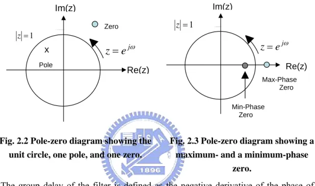
. One trip around the unit circle is equal to one FSR. A convenient graphical method for estimating a filter’s response is shown in Fig. 2.2. Zeros with a magnitude >1 are called maximum-phase, and those with magnitude <1 are called minimum-phase. A pole-zero diagram with a pair of zeros that are located reciprocally about the unit circle is shown in Fig. 2.3.Fig. 2.2 Pole-zero diagram showing the unit circle, one pole, and one zero.
Fig. 2.3 Pole-zero diagram showing a maximum- and a minimum-phase
zero.
The group delay of the filter is defined as the negative derivative of the phase of the transfer function with respect to the angular frequency as follows:
{
}
{
}
ωω
τ
τ
j e z n gz
H
z
H
d
d
T
T
= −⎥
⎦
⎤
⎢
⎣
⎡
⎟⎟
⎠
⎞
⎜⎜
⎝
⎛
−
×
=
×
=
)
(
Re
)
(
Im
tan
1 (13)where
τ
n is normalized to the unit delay, T. The absolute group delay is given byn
g
T
τ
τ
=
×
. To obtain the group delay for a single zero, considering the transfer function1 1−
(
z
)
=
1
−
re
z
−H
zero jφ wherer
andφ
are the magnitude and phase of the zero. By substitutingz
=
e
jω inH
1−zero(
z
)
, the phase is derived in terms ofr
,φ
, andω
as follows: x Re(z) Im(z) Zero Pole 1 = z ω je
z
=
Re(z) Im(z) Max-Phase Zero Min-Phase Zero 1 = z ω je
z
=
⎥
⎦
⎤
⎢
⎣
⎡
−
−
−
=
Φ
− −1
cos(
)
)
sin(
tan
1 1ω
φ
φ
ω
r
r
zero (14)[
]
)
(
1
)
(
'
)
(
tan
2 1x
g
x
g
dx
x
g
d
+
=
− (15)where
Φ
1−zero is the phase ofH
1−zero(
z
)
. From Eq. (15), the group delay simplifies to[
]
2 1)
cos(
2
1
)
cos(
)
,
(
r
r
r
r
r
zero−
−
+
−
−
=
−φ
ω
ω
φ
φ
τ
(16)Afterwards, consider the transfer function,
H
1−zero(
z
)
=
re
−jφ−
z
−1, with the reversed path, the group delay is[
]
1
(
,
)
)
cos(
2
1
)
cos(
1
)
,
1
(
2 1 1ω
φ
τ
φ
φ
ω
φ
τ
r
r
r
r
r
zero zero − −=
−
−
−
−
+
=
−
(17)The sum of the group delays is a constant value indicating that the filter has linear phase with the same magnitude response as shown in Fig. 2.4.
Fig. 2.4 Phase response of maximum and minimum phase MA filers.
8 . 0 :zzero =
Delay Delay:zzero =1.25
8 . 0 :zzero =
2.3 Interleaver
2.3.1 Interleaver technology approaches
There are three broad classes of interleaver filter technologies: lattice filter (LF), Gires-Tournois based Michelson interferometer, and arrayed-waveguide router (AWG). Within the lattice filter class there is the birefringent filter, employing birefringent crystals and classically known as a Lyot or Solc filter; the glass-based filter which substitutes an artificial polarization-dependent delay for the birefringent elements of the preceding type; and the Mach-Zehnder filter, which is the analog to the Lyot filter and is generally made with planar waveguides. Within the Gires-Tournois (GT) class there is the interference filter and the birefringent analog (B-GT). Arrayed-waveguide routers have designs for single-channel and banded filters.
2.3.2 Lattice Interleaver
Lattice filters are made from a cascade of differential-delay elements where the differential-delay of each element is an integral multiple of a unit delay and power is exchanged across paths between the elements. There are three issues to address in the study of lattice filters: the realization of the unit cell that generates the differential delay; the number of unit cells and associated intermediate power exchange; and the cascade of multiple filters.
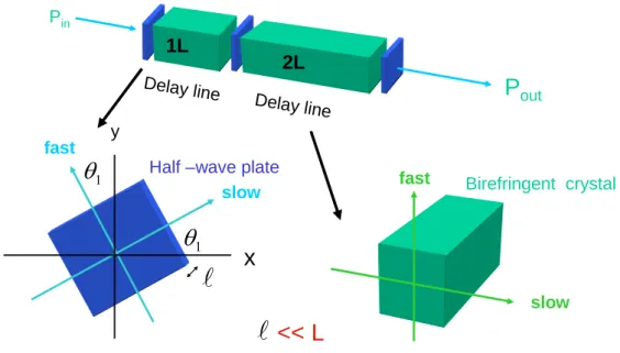
Figure 2.5 shows the configuration of the interleaver consisting of the birefringent crystals. The basic principle is based on interference between polarized light, which depends on phase retardation between the components of light polarized parallel to the slow and the fast axes of the crystal. Consequently, birefringent crystal is used to perform as optical delay, and half-wave plates are used to change the polarization direction between the delay components. An optical FIR digital filter can, thus, be made by cascading delay lines and controlling the angle of rotation between half-wave plates. The half-wave plates can also be considered to be rotated to generate require Fourier frequency components.
1
θ
2L 1L slow fast Delay line Delay line 1θ
fast slowHalf –wave plate
Birefringent crystal
<< L
yx
P
out PinFig. 2.5 Brief configuration of an L-2L interleaver
Actually, the design goal is to generate a periodic rectangular function as displayed in Fig. 2.6.
The function could be defined as
) 100 ( ) ( , 50 25 , 0 25 25 , 1 25 50 , 0 ) ( = + ⎪ ⎩ ⎪ ⎨ ⎧ < < < < − − < < − = y f y f f f f f y (21)
Expand it to Fourier series; there is no even function term. The constant
a
0 anda
n is retained.ω
)
(
ω
f
Expand to Fourier series
1
Fig. 2.6 The periodic rectangular function
y( f )
3 , 2 , 1 , ) 2 sin( 2 ) 2 cos( 1 100 1 2 1 1 200 1 50 50 50 50 0 = = ⋅ ⋅ = = ⋅ =
∫
∫
− − n n n df f n a df a nπ
π
π
(22)Therefore, the final rectangular function could be written as Eq. (23)
+
×
⋅
−
⋅
+
=
cos(
2
)
cos(
3
2
)
2
1
)
(
f
a
1f
a
3f
y
π
π
(23)Here we know that the square-wave amplitude function has only odd Fourier frequency components with appropriate Fourier coefficients.
According to the Jones matrix theory [12], a half-wave plate has a phase retardation of
π
=
Γ
, and the thickness of =λ/2(ne−no). The Jones matrix for the half-wave plate is obtained by using Eq. 24.⎥
⎦
⎤
⎢
⎣
⎡
−
−
=
0
0
i
i
W
hp (24) We can write the Jones matrix for the delay line as⎥
⎥
⎦
⎤
⎢
⎢
⎣
⎡
=
− dnL i dnL i delaye
e
W
2 20
0
ω ω (25)where
L
is the length of the delay-line crystal anddn
is the difference between then
eand
n
o (the indices of the ordinary and extraordinary axes).In the figure below, the Jones matrix for the incident beam can be written as
[
1
;
0
]
to specify the input light is linearly polarized on the x axis. By adjusting the angles of the half-wave plates appropriately, we can get the odd channels and even channels lying the x and y axes, respectively, at the output port.in hp L hp L hp out
W
W
W
W
W
P
P
=
(
22
.
5
°)
*
2(
ω
)
*
(
θ
2)
*
(
ω
2
)
*
(
θ
1)
*
Change the angle of the two half-wave plates to fit the Fourier seriesFor Example: 1L-2L 2 ω Whp( ) Whp( ) 1 θ 2 θ L 2L Pout [1; 0] Pin 1 θ 2 θ WL( )
ω
Whp( pi/8 ) W2L( )ω
Whp( pi/8 ) W2L( ) Odd channel Even channel⎥
⎥
⎦
⎤
⎢
⎢
⎣
⎡
− dnL i dnL ie
e
2 20
0
ω ω 2 2 1(22.5 )
( )
( )
(
2
)
( )
out hp L hp L hp inP
=
W
° i
W
ω
i
W
θ
i
W
ω
i
W
θ
i
P
By combining all Jones matrices of the birefringent crystals, we can write the transmission as
2 1
(22.5 ) (2 ) ( ) ( ) ( )
out hp delay hp delay hp in
E =W ° iW L Wi
θ
iW L Wiθ
iE (26) where Wdelay( L2 ) andW
L(L) are the Jones matrices of the two crystalsNevertheless, how to get the angles to fit the Fourier coefficients in Eq. (22) is the critical point. Utilizing the optimization tools in Matlab programs is the solution. The goal is to minimize the error function by sweeping the half-wave plate angles as
( ) ( )
( ) ( )
( ) ( )
( )( )
∫
∫
∫
− = − = − = − = 2 1 2 2 1 2 1 2 10 2 log max w w w y w w w w dw w x error dw w x w y error dw w x w y error w x w y error2
,
2
2 1FSR
w
w
FSR
w
w
=
c−
=
c+
(27)where
x
(w
)
is the target or ideal square periodic function and the y(w) is real transmission function. The transmission function is periodic, so the errors are only summed over one FSR at the central frequency,w
c [13]. The last three approximation criteria include errors at all points of frequency in the interval; therefore, they include more error datathan the first for each
y
(w
)
considered. We choose the last approximation criterion because it is the energy in the error signal. [14]2.3.3 Mathematical Derivation
Here we use the easiest case: one stage interleaver includes a delay line and two half-wave plates in which the second plate is determined to 22.5 degree. Assume that there
is an incident beam
V
x(=⎥
⎦
⎤
⎢
⎣
⎡
0
1
) injected to the first half-wave plate, then the Jones matrix
1
M
at the output can be written as(
a and a arereal numbers)
a a j e e e e e e M j j j j j j 2 1 2 2 1 1 1 1 2 1 1 2 1 2 2 1 2 2 1 1 1 1 2 2 1 1 1 1 1 ) ( ) ( sin cos sin cos sin cos 0 1 cos sin sin cos 0 0 cos sin sin cos ⎥ ⎦ ⎤ ⎢ ⎣ ⎡ ⋅ = ⎥ ⎥ ⎥ ⎦ ⎤ ⎢ ⎢ ⎢ ⎣ ⎡ − + = ⎥ ⎦ ⎤ ⎢ ⎣ ⎡ ⋅ ⎥ ⎦ ⎤ ⎢ ⎣ ⎡ − ⋅ ⎥ ⎥ ⎦ ⎤ ⎢ ⎢ ⎣ ⎡ ⋅ ⎥ ⎦ ⎤ ⎢ ⎣ ⎡ − = − − − θ θ θ θ θ θ θ θ θ θ θ θ θ θ θ θ π π π π π π (28)
where the undetermined angle is set to be a variable
θ
1. RegardM
1 as the emerging beam and let it inject into the crystal of length L. The new Jones matrixM
2is obtained byusing Eq. (29).
⎥
⎥
⎥
⎦
⎤
⎢
⎢
⎢
⎣
⎡
⋅
=
⎥
⎦
⎤
⎢
⎣
⎡
⋅
⋅
⎥
⎥
⎥
⎦
⎤
⎢
⎢
⎢
⎣
⎡
⋅
=
− − − c c c c df f j df f j df f j df f j je
a
e
a
j
a
a
j
e
e
e
M
π π π π φ 2 1 2 1 20
0
(29)In Eq. (29),
df
c is the channel spacing andφ
is equal todn
ω
L
/
2
c
. The phase factorφ
j
e
− can be neglected if interference effects are not important, or not observable. Then use2
M
to multiply the second half-wave plate (⎥
⎦
⎤
⎢
⎣
⎡
−
=
°X
Y
Y
X
j
W
22.5 ,X
andY
are real⎥
⎦
⎤
⎢
⎣
⎡
=
⎥
⎥
⎥
⎦
⎤
⎢
⎢
⎢
⎣
⎡
−
+
−
=
⎥
⎥
⎥
⎦
⎤
⎢
⎢
⎢
⎣
⎡
⋅
⎥
⎦
⎤
⎢
⎣
⎡
−
=
⋅
=
− − − ° y x df f j df f j df f j df f j df f j df f jE
E
Ye
a
Xe
a
Ye
a
Xe
a
e
a
e
a
j
X
Y
Y
X
j
M
W
M
c c c c c c π π π π π π 2 1 2 1 2 1 2 5 . 22 3 (30)In Eq. (30), we arbitrarily choose
E
xorE
y and square it to obtain the Eq. (31).[
]
{
}
c c c x x x df f Y Xa a Y a X a df f Y a X a df f Y a X a E E T π θ θ θ θ π π 2 cos ) ( ) ( 2 ) ( ] ) ( [ sin ) ( cos ) ( 1 2 1 1 2 2 2 2 1 1 2 2 2 1 2 2 2 1 * + + = − + + = ⋅ = (31)Compare with Eq. (23), the first term needs to equal 1/2 and the coefficient of the second term needs to equal the Fourier coefficient by optimizing the angle of
θ
1. By this way, we can easy to understand the theory of interleaver.2.3.4 Interleaver Simulation Results & Practical Device Measurement
The lengths of delay-line crystals in the program are determined using Eq. (32).
FSR
spacing
Channel
df
mc
dn
f
L
dnL
c
m
f
c c c=
=
=
⇒
=
(32)In Eq. (32),
c
is the speed of light;f
c is the central frequency in the range of operation frequencies;m
is the order of the birefringent wave plate.L-2L Interleaver
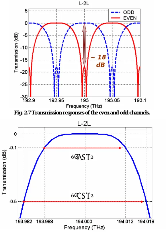
The found angles for two half-wave plates are 7.7356 and 29.5286 degrees. Figure 2.7 shows the transmission responses of the even and odd channels; the isolation is about 18 dB.
Fig. 2.7 Transmission responses of the even and odd channels.
Fig. 2.8 The bandwidth estimations of -0.1dB and -0.5dB for L-2L interleaver.
The ripple is about 0.0026 dB; the bandwidths of -0.1dB and -0.5dB are 24 GHz and 36 GHz, respectively, as shown in Fig. 2.8.
~ 18
dB
~24 GHz
Fig. 2.9 Dispersion compensating interleavers for add/drop node
In Fig. 2.9, the path with the negative group delay is called Type-I here, and another path with the positive group delay is called Type-II. The Type-I and Type-II have the same transmission response.
The corresponding parameters for simulation are given below: Central wavelength = 193.00 THz;
Difference of index between n0 and ne=0.2138; C = 2.997925x10⁸ m/s;
Channel spacing = 100 GHz;
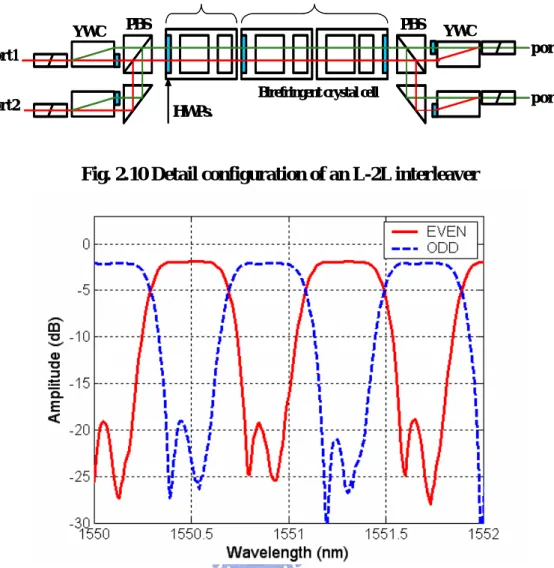
The interleaver we used is a symmetrical four-port interleaver with two input and two output ports. The detail configuration is shown in Fig. 2.10. It incorporates the birefringent crystal cells; half wave plates (HWP), YVO4 walk off crystals (YWC) and polarization beam splitters (PBS).
L 2L
PBS
HWPs.
Birefringent crystal cell port1 port2 port3 port4 (a) YWC PBS YWC L 2L PBS HWPs.
Birefringent crystal cell port1 port2 port3 port4 (a) YWC PBS YWC
Fig. 2.10 Detail configuration of an L-2L interleaver
Fig. 2.11. Measured amplitude response of the interleaver for even and odd channels
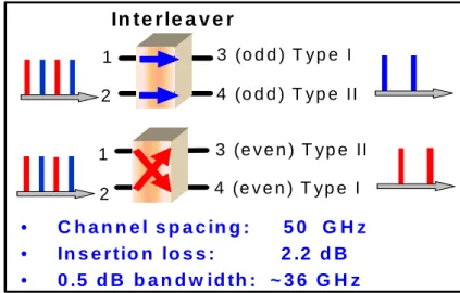
Figure 2.11 illustrates the measured amplitude response of the interleaver for even and odd channels. The channel spacing of this interleaver is 50-GHz with insertion loss of 2.2-dB and 0.5-dB pass bandwidth of around 36-GHz, respectively. The two mirrored corresponding group delay curves are measure by the channel analyzer (Q7760), shown in figure 2.12(a) and figure 2.12(b).
Fig. 2.12(a). Amplitude response and the corresponding group delay of the interleaver for odd channels (type II)
Fig. 2.12(b). Amplitude response and the corresponding group delay of the interleaver for even channels (type I)
1 2 3 (o d d ) T y p e I 4 (o d d ) T y p e II 1 2 3 (e v e n ) T y p e II 4 (e v e n ) T y p e I In te r le a v e r • C h a n n e l s p a c in g : 5 0 G H z • In s e r tio n lo s s : 2 .2 d B • 0 .5 d B b a n d w id th : ~ 3 6 G H z
2.4 Application of using an Interleaver in bi-directional amplification
We design the interleaver to have complementary wavelength dependent routing characteristics. For example, if λ1 (odd/west channel) enters port 1, it will be routed to port 3. On the other hand, when λ2 (even/east channel) goes into port 2; it will also be directed to port 3. A more detail wavelength routing diagram is displayed in Fig. 2.14.
Fig. 2.13. Passband of the interleaver for even and odd channel
Such interleaving property is exploited to route simultaneously both the even channels, which arrive at the interleaver at port 2; and the odd channels, which enter the interleaver at port 1, to port 3. Therefore, the even and odd channels, which propagate in opposite directions, can be transformed into a co-propagating transmission in a single amplification section to achieve unidirectional amplification using a single EDFA, as shown in Fig. 2.15. The proposed innovative interleaving configuration not only supports the use of a single EDFA to achieve bidirectional transmission, but also eliminates the presence of a dead zone in the blue-red splitting technology due to this interleaver is implemented to cover the whole C band (1530 nm to 1560 nm), thus further increases the bandwidth utilization.
Fig. 2.14. Transmission of Interleaver West (Odd) East (Even) DCF EDFA EDFA Interleaver East West
Fig. 2.15. Wavelength re-routing scheme for bidirectional transmission
Along side with bidirectional amplification function, dispersion compensation issue is also considered in this wavelength re-routing scheme. As described in Fig. 2.13, the group delay of routing port 2 to port4 and port 1 to port 3 are a pair of mirrored group delay and vice versa in the case of port 2 to port 3 and port 1 to port 4. The group delay of Type I and Type II
are displayed in Fig. 2.16(a), as well as the group delay after connecting Type I and Type II. Consequently, the wavelength re-routing scheme not only benefits bidirectional amplification but also provides a dispersion compensated environment.
Fig. 2.16 (a) In-band group delay for two types of interleaver, (b) group delay of cascading Type I and Type II.
Chapter 3
Experiment of bi-directional straight line
transmission
3.1 Bidirectional Optical Amplifier Configurations
Optical amplifiers are usually equipped with optical isolator, which make them unsuited for bidirectional transmission, in principle. However, it is possible to construct optical amplifiers for bidirectional transmissions. In the following section, we will consider the configuration of bidirectional optical amplifiers.
The simplest configuration for an optical amplifier is obtained by just omitting the optical isolators; since the operation of optical amplifiers is reciprocal. However, when a single EDFA (optical amplifier) is used bidirectionally without optical isolators or filters, interaction between the bidirectional channels may occur. There are at least three mechanisms for this interaction.
Reflections and Rayleigh backscattering cause crosstalk between bidirectional channels. A bidirectional amplifier will enhance this crosstalk, since it amplified the reflected signal.
Gain saturation will also cause mutual interaction, since if the signal in one direction saturates the gain, the signal in the other direction will also experience gain saturation.
Similarly the signal in one direction may influence the noise behavior of the optical amplifier for the signal in the other direction.
The omission of the optical isolators makes the bidirectional amplifier less expensive than a conventional unidirectional amplifier. However, several other configurations have been proposed in literature, see Fig. 3.1
(EDFA) in a circuit, which combines and separates the bidirectional signals with wavelength splitters. The application of WDM makes this bidirectional amplifier configuration insensitive to optical reflections.
Ref. [16] uses a combination of two wavelength splitters and two optical isolators to have both optical isolation at all wavelengths, and bidirectional transmission.
Ref. [17], [18] and [19] propose the use of two separate EDFAs to decouple the saturation in the two directions. Here, each EDFA can have optical filters and isolator(s) or circulators.
Fig. 3.1 (a) Bidirectional amplification with unidirectional optical amplifier (b) Bidirectional amplifier with optical isolation (c) double optical amplifier with shared
3.2 Non-linear effects
The response of any dielectric to light becomes nonlinear for intense electromagnetic fields, and optical fiber are no exception. On a fundamental level, the origin of nonlinear response is related to anhormonic motion of bond electrons under the influence of an applied field. As a result, the induced polarization P from the electric dipoles is not linear in the electric field E, but satisfies the more general relation
...} :
{ (1) (2) (3)
0 ⋅ + + +
= E EE EEE
P ε χ χ χ , where ε0 is the vacuum permittivity and χ( j)
(j=1,2,3,…) is j th order susceptibility. To account for the light polarization effects, χ( j) is a
tensor of rank j+1. The linear susceptibility χ(1) represents the dominant contribution to P.
Its effects are included through the refractive index n and the attenuation coefficientα .
The nonlinear effects governed by the third-order susceptibility χ(3) are elastic in the
sense that no energy is exchanged between the electromagnetic field and the dielectric medium. Thus, a second class of nonlinear effects results from stimulated inelastic scattering in which the optical field transfers part of its energy to the nonlinear medium. Two important nonlinear effects in optical fiber fall in this category; both of them are related to vibrational excitation mode of silica. These two phenomena are known as stimulated Raman scattering (SRS) and stimulated Brillouin scattering. The fundamental difference is that SBS in optical fiber occurs only in the backward direction whereas SRS dominates in the forward direction. Another nonlinear effect called Rayleigh backscattering (RB) will also deteriorate the bidirectional transmission system. Because any backward scattering will interfere the backward signal directly, the following discussions will focus on SBS and RB effects.
3.2.1 Stimulated Brillouin scattering
Stimulated Brillouin scattering can be understood as scattering of a photon to a lower energy photon such that the energy difference appears in the form of a phonon. The special
characteristics of SBS are the participation acoustic phonons and it only occurs in backward direction. In stimulated Brillouin scattering, the cross section is sufficiently small that loss is negligible at low power levels; however, at high power levels, the nonlinear phenomena of stimulated Brillouin scattering become important.
Thy physical process behind Brillouin scattering is the tendency of materials to become compressed in the presence of an electric field – a phenomenon termed electrostriction [20]. For an oscillating electric field at the pump frequency, ωp, this process generates an acoustic
wave at some frequency, ωA. Spontaneous Brillouin scattering can be viewed as scattering of the pump wave from this acoustic wave, resulting in creation of a new wave at the pump frequency, ωs . Since the scattering process must conserve both the energy and the momentum, the frequency and the wave vectors of the three waves are related by:
s p A s p A
κ
κ
κ
ω
ω
ω
−
=
−
=
, (33)Where κp and κs are the wave vectors of the pump and Stoke waves. Using the dispersion
relation | | A A
A
ω
κ = ν , where νA is the acoustic velocity, this condition determines the
acoustic frequency as Eq. (33): | | 2 | | sin( / 2)
A A A A p
ω =κ ν = ν κ θ (34)
Where |κp | |≈κs|was used and θ represents the angle between the pump and scattered waves.
Note that ωA vanishes in the forward direction (θ=0) and is maximum in the backward direction (θ=π). In single-mode fibers, light can travel only in the forward and backward directions. As a result, SBS occurs in the backward direction with a frequency shift
2
B A kp
ω = ν , using p 2
P
n
k = π λ , where λP is the pump wavelength, the Brillouin shift
2 2 B A B P n ω ν ν = π = λ
Where n is the mode index. Using νA=5.96 km/s and n=1.45 as typical values for silica
fibers, νB ≅11.1 GHz at λp=1.55μm.
All in all, we control the input powers under 6-dBm injected into the transmission fiber without performance degradation resulting from SBS.
3.2.2 Rayleigh backscattering
A fundamental effect observed in optical fibers is Rayleigh backscattering: light bounces off microscopic defects in the amorphous structure of the glass. These defects (much smaller than the wavelength of the light) scatter the light and give rise to attenuation. Some of the scattered light returns along the fiber. The light scattered from a larger distance along the optical fiber contributes less to the total amount of returning light than scattering near the fiber input, because of attenuation in the fiber.
The magnitude of Rayleigh backscattering is derived by considering a uniformly backscattering fiber of length L. After being coupled into the input of the fiber, a unit energy optical impulse of power δ( )t propagates in the forward direction. Notice that in this section
only light intensities are used, because the different contributions to the Rayleigh backscattering add incoherently. The power propagating in the reverse direction, prior to being coupled out at the same input end, is the backscattered impulse response power
2 0 , ( ) 0 gt g L be for t h t otherwise αν ν − ⎧ ≤ ≤ ⎪ = ⎨ ⎪ ⎩ (35)
Here t is the round-trip transit time of the light out to a point ( 1 2
g
z
t
ν
= i ) along the fiber and back. The fiber parameters above are,
g
ν = group velocity = c/n (km/s), where cg ≅ 2.998×10⁵ km/s
g
n = group index (dimensionless)
b = backscatter parameter = (νg/2)βsF (Watt/Joule)=(1/s)
s
β = scattering coefficient (1/km)
F = backscatter capture fraction (dimensionless)
All these parameters are taken to be essentially uniform along the fiber. They depend on fiber type and on wavelength. The parameter b at a point along the fiber is the backscattered propagating power corresponding to a unit incident energy. The parameter F is the fraction of the scattered power that is captured as backward propagating power. It depends on other standard fiber parameters such as the mode-field diameter.
For an input power signal p(t), the backscattered response at the input end is the convolution with the impulse response of Eq. (35):
( ) ( ) ( ) r t hτ p t τ τd ∞ −∞ =
∫
− 2 / 0 ( ) g g L b e p t d ν αν τ τ τ − =∫
− (36)Applying this result to the situation of an optical continuous wave, the input power is a steady value p(t)=p0. Substituting this into (36) yields the continuous response r(t)= r0 that depends on the fiber type and length: 2
0( ) 0 (1 ) g L bn r L p e c α α −
= − . For short fiber length, the
backscatter fraction is 0 0 2 ( ) ( ) r L bng B L p c = ≈ (37)
Whereas for long fiber length, the backscatter fraction is
0 0 ( ) ( ) r L bng B p cα ∞ = ≈ (38)
This backscatter fraction equals approximately -32 dB for a single mode fiber at 1550 nm. This level can be used as a reference when specifying the reflection of a connector or splice. In general, the Rayleigh backscattering at the facet of a connector or splice is a minor factor
of performance deterioration.
Fig. 3.2. Scheme of crosstalk due to single- and double-amplified RB of signal as well as ASE. PASE is the power of ASE noise from the EDFA. Esd is the downstream signal, and Esu is the upstream signal. ERBd and ERBu are the
Rayleigh backscattered signals of Esd and Esu , respectively.
However, as illustrated in Fig. 3.2, with the Rayleigh backscattering induced crosstalk, bidirectional amplifier node is susceptible to occurrences of self-oscillation; distributed Rayleigh mirrors are forming optical cavity with enclosed amplifier gain, thus, providing necessary conditions for node lasing. Therefore, under the circulator based bidirectional amplifier, Rayleigh backscattering effect would be an degradation factor not only deteriorates the transmission performance but also limits the gain of the this bidirectional amplifier configuration.
3.3 Experimental setup & results of bidirectional straight line transmission
In order to achieve bidirectional transmission, we build up a transmission system with the utilization of the wavelength re-routing characteristic of the four-port interleaver. The experimental setup is illustrated in Fig. 3.3. We use a dual-stage EDFA with mid-stage