國 立 交 通 大 學
材料科學與工程學系
博 士 論 文
表面微結構對氮化鎵發光二極體光電特性之影響
Effects of Surface Microstructures on the Optoelectronic
Properties of GaN-based Light-Emitting Diodes
研 究 生:廖 崢
指導教授:吳耀銓 博士
表面微結構對氮化鎵發光二極體光電特性之影響
Effects of Surface Microstructures on the Optoelectronic Properties of
GaN-based Light-Emitting Diodes
研 究 生:廖 崢 Student:Cheng Liao
指導教授:吳耀銓 博士 Advisor:Dr. YewChung Sermon Wu
國 立 交 通 大 學
材料科學與工程學系
博 士 論 文
A Thesis
Submitted to Department of Material Science and Engineering College of Engineering
National Chiao Tung University in partial Fulfillment of the Requirements
for the Degree of Doctor of Philosophy
in
Material Science and Engineering February 2010
Hsinchu, Taiwan, Republic of China
I
表面微結構對氮化鎵發光二極體光電特性之影響
學生:廖 崢 指導教授:吳耀銓 博士
國立交通大學材料科學與工程研究所博士班
摘要
本論文主旨為探討與增進氮化鎵發光二極體(GaN-Based Light-Emitting Diode, GaN-LED)表現相關的議題,包括了鏡面在元件中的位置對於發光功率的影響、n型氮化鎵 碗狀結構與鏡面的結合在調變發光角度過程中所扮演的角色,以及利用自然微影方式對氧 化銦錫透光層做表面粗化的結果探討。 在鏡面於元件中的位置對於發光功率影響的實驗中,我們發現DRSM-LED(LED結構 包含雙粗化表面以及鍍附於藍寶石基板底面的鏡面結構)的發光強度為PR-LED(LED結構 包含單一p型氮化鎵的粗化表面)的2.10倍。當改變鏡面位置將其從藍寶石基板底面移至無 參雜氮化鎵與藍寶石基板的介面(即DRM-LED)時,發光強度得到了更大的提升(為PR-LED 的3.05倍)。這是由於在DRSM-LED中,光子必須比在DRM-LED中多穿越額外的接合界面 (環氧化物/藍寶石基板)兩次。此外,當往元件底部行進的光子被DRSM-LED的鏡面改 變方向回到環氧化物/藍寶石基板的界面時,只有光徑在臨界角61.9°以內才能夠穿越,大 於臨界角的部分會於藍寶石基板內形成全反射而損失。 在NBM-LED(LED結構包含p型氮化鎵粗化表面,以及n側碗型結構與鏡面結合的表面) 的實驗中,我們利用三種不同尺寸的碗狀結構來調變發光角度與增進元件表現。我們發現 發光強度與發光功率會隨著n側碗型結構尺寸的縮小而提升,其中以3微米者為最佳,其發
II 光強度與功率為PR-LED的2.33與1.43倍。此外,NBM-LED的發光角度會隨著n側碗型結構 尺寸的縮小而縮小,由PR-LED的130°縮小至3微米碗狀結構元件的118°,這是由於碗狀結 構與鏡面的結合可視為凹面鏡,此凹面鏡不但可以將往元件底面行進的光子導至正面,且 可將光徑在臨界錐形區外的光子修正回圓錐內。 在氧化銦錫透光層的粗化方面,我們提供了一種簡單而有效的自然微影法用以製作 GaN-LED。此法是將不同塗佈厚度的光阻作為感應耦合電漿(ICP)乾蝕刻製程的結構轉 印模具,於蝕刻過程中,光阻表面會因熱累積而產生縐折,此縐折並於其後轉印至氧化銦 錫上。不同粗化程度的元件,其發光強度與功率皆高於傳統GaN-LED。以1.9微米光阻製作 的元件,發光強度(71.6 mcd)為傳統LED的1.5倍,且為1.6微米的1.2倍。在發光功率方面, 1.9微米光阻製作的元件(5.75 mW)約為傳統LED的1.27倍,且為1.6微米的1.07倍。這是因 為粗化的氧化銦錫不但提供光子更高的機率穿越LED表面,而且具有改變光子路徑的優點。
III
Effects of Surface Microstructures on the Optoelectronic Properties of
GaN-based Light-Emitting Diodes
Student : Cheng Liao Advisor : Dr. YewChung Sermon Wu
Department of Materials Science and Engineering
National Chiao Tung University
ABSTRACT
The primary contents of this dissertation are discussing subjects which are relating to the performance enhancement of InGaN-GaN light-emitting diodes, including the influence of the mirror location to the light output, the role of the n-bowl/mirror structure played in managing the view angle, and the roughening of the ITO window layer by a natural lithography method.
In the investigation of the effect of the mirror location on the performance of LEDs, we found that the light intensity of DRSM-LED (LED with double-roughened surfaces and a mirror system on the back side of sapphire substrate) was 2.10 times higher than that of PR-LED (LED with roughened p-GaN surface). By changing the mirror location from the backside of the sapphire to the u-GaN/sapphire interface (DRM-LED), the LED light intensity was further enhanced (3.05 times higher than the PR-LED). This is because, compared with DRM-LED, the photon path inside the DRSM-LED structure has to pass through an extra bonded interface (epoxy/sapphire) 2 times. Besides, when the mirror of DRSM-LED redirecting the downward-traveling light, light traveling from sapphire to the adhesive layer will only cross within a critical angle of 61.9°. The light reaching the adhesive layer beyond the critical angle will undergo total internal reflection.
IV
and mirror on the n-bowl surface.) were introduced to adjust the view angle and improve the LED performance. We found that the light intensity and output power of NBM-LEDs increased with the decrease in n-bowl dimension. The luminance intensity and output power of the NBM-LED with 3 μm n-bowl were the highests, which were 2.33 and 1.43 times higher than PR-LED. Besides, the view angle decreased with the diameter of n-bowl. The viewing angle of PR-LED was 130°. As the diameter of n-bowl decreased to 3 μm, the view angle decreased to 118°. This is because the n-bowl mirror structure acting as a concave mirror. It not only reflected the downward photons to the front side, but also redirected the photons which were originally emitted out of the escape cone, back into the escape cone.
An investigation of the relationship between ICP etching conditions and LED performance has led to the development of a simple, effective natural lithography process for preparing ITO-textured surfaces useful for fabricating high-brightness GaN-based LEDs. In this lithography process, photoresist layers (AZ-1518) of different thicknesses (1.6 and 1.9 μm) were used as a mask for ICP dry etching. During etching, surface of the photoresist deformed because of the thermal accumulation, and this undulation was subsequently transferred to ITO surface. The light intensity and output power of IR-LEDs were better than those of the CV-LED. The luminance intensity of the IR1.9-LED was 71.6 mcd, which was 1.5 times higher than that of the CV-LED, and 1.2 times higher than that of the IR1.6-LED. The IR1.9-LED achieved an output power of 5.75 mW, which was 1.27 times higher than that of the CV-LED, and 1.07 times higher than that of the IR1.6-LED. This is because the roughened ITO surface provided the photons multiple opportunities to escape from the LED surface, and redirected the photons.
V
誌 謝
六年半是一段很長的歲月,雖然時光已消逝,但初衷仍深刻烙印心中,很慶幸 當初做了明確的決定,且信願堅定,才能走到這一步。過程雖然溝壑滿佈,但在許 多人的幫助之下,問題總算一一解決,達成了以往認為遙不可及的夢想。 心中最深沈的感謝,往往難以用言語清楚的表達。很感謝指導老師吳耀銓教授 在這段時間中對我的關懷,即便我曾因興趣乖離而躊躇喪志,老師仍給予包容,並 帶領著我走到最後。研究上除了指引正確的道路、觀念傳授,同時也給我們保留了 很大的發揮空間,讓創意發展之餘,知識也不斷成長。 研究能夠完成,實驗室的同學們也給了我很大的協助。感謝彭偉智、劉柏均學 長,以及陳一凡、彭顯智、林廷政、鄭季豪、黃秉緯、林博文、謝承佑、徐志偉、 吳騏廷、王寶明、張志榜、陳建誌等學弟,有了他們的幫忙,許多棘手的問題才得 以解決。同時很感謝晶元光電的葉瑞鴻經理,以及世欽、騰輝、曉惠等人,有他們 無私的付出,元件才得以完成。 最感謝的是我的父母廖運偉先生與陳月映女士,在我求學的路上不斷的給予支 持,讓我免除後顧之憂,否則博士學業必定無法達成。感謝弟弟廖嶸成為精神依靠, 在人生路上能夠相伴。最後還要感謝我的妻子林慧菁與女兒廖辰,多虧有他們一直 以來默默的支持與鼓勵,我才能夠堅持至今。今後我將盡我所能,榮耀我最愛的家 人!VI
CONTENTS
摘要... ... I ABSTRACT.... ... III 誌謝... ... V CONTENTS.... ... VI FIGURE LIST ... IX TABLE LIST... ... XIICHAPTER 1 INTRODUCTION ... 1
1.1 Progress of the Lighting ... 1
1.2 Light-Emitting Diodes ... 3
1.2.1 Historical Introduction ... 3
1.2.2 Advantages of the LED Lighting ... 5
1.2.3 Applications ... 7
1.3 III-V Nitride Based LEDs... 10
1.4 Issues of Nitride Based LEDs ... 11
1.4.1 Joule Heating Problem ... 11
1.4.2 Fresnel Reflection ... 12
1.4.3 Total Internal Reflection ... 13
1.5 An Overview of the Dissertation ... 14
CHAPTER 2 BACKGROUND AND THEORY ... 20
2.1 Basics of LEDs ... 20
2.1.1 Device Configuration ... 20
2.1.2 Recombination of Electrons and Holes ... 21
VII
2.1.4 Electroluminescent Structure ... 23
2.1.5 Efficiency ... 24
2.2 Snell’s Law ... 26
2.3 Reflection Losses of Light ... 27
2.3.1 Total Internal Reflection ... 27
2.3.2 Fresnel Loss ... 28
2.4 Concave Mirror ... 29
2.5 Transmission Line Model (TLM) ... 30
2.6 Wafer Bonding ... 32
CHAPTER 3 EFFECT OF THE SILVER MIRROR LOCATION ON THE LUMINANCE INTENSITY OF DOUBLE-ROUGHENED GAN LIGHT-EMITTING DIODES ... 43
3.1 Introduction ... 43
3.2 Experiments ... 44
3.2.1 Illustration and abbreviation of LEDs ... 44
3.2.2 Crystal growth and device process of PR-LED ... 44
3.2.3 Fabrication of DRM- and DRSM-LEDs ... 45
3.3 Results and Discussions ... 46
3.4 Summary ... 48
CHAPTER 4 IMPROVED PERFORMANCE OF INGAN-GAN LIGHT-EMITTING DIODE BY A PERIODIC N-BOWL MIRROR ARRAY ... 58
4.1 Introduction ... 58
4.2 Experiments ... 59
4.2.1 Illustration and Abbreviation of LEDs ... 59
4.2.2 Crystal Growth and Device Process of PR-LED ... 59
4.2.3 Fabrication of NBM-LEDs ... 60
VIII
4.4 Summary ... 63
CHAPTER 5 INGAN-GAN LIGHT-EMITTING DIODE PERFORMANCE IMPROVED BY ROUGHENING INDIUM TIN OXIDE WINDOW LAYER VIA NATURAL LITHOGRAPHY ... 76
5.1 Introduction ... 76
5.2 Experiments ... 77
5.2.1 Illustration and Abbreviation of LEDs ... 77
5.2.2 Fabrication of the CV- and IR-LEDs ... 77
5.3 Results and discussions ... 78
5.4 Summary ... 81
CHAPTER 6 CONCLUSIONS AND FUTURE WORKS ... 92
6.1 Conclusions ... 92 6.2 Future Works ... 93 REFERENCE. ... 95 Chapter 1 ... 95 Chapter 2 ... 97 Chapter 3 ... 97 Chapter 4 ... 98 Chapter 5 ... 99
IX
FIGURE LIST
Figure 1.1 (a) Illustration of the nightly illumination of a gaslight with a thorium oxide–soaked mantle. (b) Original carbon-filament bulb from Thomas Edison. (c) A closeup of a 175W mercury vapor lamp. (d) An early compact fluorescent lamp.... ... 16 Figure 1.2 Bandgap energy of various materials for visible emission devices as a function of their lattice constant. ... 17 Figure 1.3 Chromaticity diagram. White light can be produced through color mixing, like
red/blue/green, blue/yellow, or green/yellow-green/orange/purple. ... 18 Figure 2.1 The schematic of a typical surface-emitting LED... 34 Figure 2.2 Intrinsic radiative transitions in semiconductors. (a) Band-to-band transitions; (b) free-exciton annihilation; (c) recombination of exciton localized at band-potential fluctuations. ... 35 Figure 2.3 Band structure near a semiconductor p-n homojunction: (a) under zero bias; (b)
under forward bias. ... 36 Figure 2.4 Band alignment diagram of a quantum well structure. ... 37 Figure 2.5 Behavior of light when traveling between two different mediums. Both reflection and refraction occur. ... 38 Figure 2.6 Illustration of the physical parameters of the concave mirror. ... 39 Figure 2.7 (a) Schematic illustration of the TLM patterns. (b) Plot of total contact as a function of L to obtain transfer length and contact resistance values. ... 40 Figure 2.8 Three situations when two wafers contact with each other. ... 41 Figure 2.9 (a) Diffusion occurred because of the difference of surface curvature. (b) Interface after annealing. ... 42 Figure 3.1 Schematic diagrams of (a) PR-LED, (b) DRSM-LED, and (c) DRM-LED. ... 50 Figure 3.2 Fabrication process of the PR-LED. ... 51
X
Figure 3.3 Experiment flowchart. ... 52
Figure 3.4 Reflectivity of different mirrors. ... 53
Figure 3.5 SEM image of the u-GaN surface etched by 90oC KOH for 1 min. ... 54
Figure 3.6 I-V characteristic of the LEDs. ... 55
Figure 3.7 The effects of injection current on the luminous intensity of the LEDs. ... 56
Figure 3.8 Possible photon paths inside the structures of the (a) DRSM-LED and (b) DRM-LED. ... 57
Figure 4.1 Schematic illustration of LEDs: (a) PR-LED, (b) NBM-LED, and (c) the n-bowl mirror array of the 25-4 NBM-LED. (d) is the cross-sectional SEM image of the 4-3 n-bowl structure. ... 64
Figure 4.2 Fabrication process of the PR-LED. ... 66
Figure 4.3 Experiment flowchart. ... 67
Figure 4.4 SEM image of the 4-3 n-bowl structure. ... 68
Figure 4.5 Current-voltage characteristic of the LEDs. ... 69
Figure 4.6 The effects of injection current on the luminous intensity of the LEDs. ... 70
Figure 4.7 Illustration of the physical parameters of the bowl. The bowl has radius r, height h, and R is the radius of the complete sphere. ... 71
Figure 4.8 The effects of injection current on the light output of the LEDs. ... 72
Figure 4.9 The radiation patterns of LEDs. ... 73
Figure 4.10 Illustration of the physical parameters of the concave mirror ... 74
Figure 4.11 Schematic illustration of the n-bowl structure ... 75
Figure 5.1 Schematic diagrams of the (a) CV-LED, (b) IR-LED. ... 83
Figure 5.2 Experiment flowchart. ... 84
Figure 5.3 SEM images of ITO surfaces: (a) CV-LED, (b) IR1.6-LED, and (c) IR1.9-LED. (d) is the surface morphology of the 1.9-μm-thick photoresist after 4 min ICP etching. ... 86
XI
Figure 5.4 AFM images of ITO surfaces: (a) CV-LED, (b) IR1.6-LED, and (c) IR1.9-LED.... ... 87 Figure 5.5 Current-voltage characteristic of the LEDs. ... 88 Figure 5.6 The effects of injection current on the luminous intensity of the LEDs. The
emission peak wavelength of the LEDs was 461 nm. ... 89 Figure 5.7 The effects of injection current on the light output of the LEDs. ... 90 Figure 5.8 Light distribution of LEDs as a function of the detection angle. ... 91
XII
TABLE LIST
Table 1.1 Thermal conductivity of the materials. ... 19 Table 4.1 The parameters and performances of LEDs. ... 65 Table 5.1 The specific contact resistance ρc of samples A-E. ... 85
1
CHAPTER 1
INTRODUCTION
1.1 Progress of the Lighting
Up to the nineteenth century, flame produced by combustion was the only source of artificial light. Combustion results in the excitation of atoms and molecules. The emission is caused by radiative transitions in excited atoms and ions, recombination of ions to form molecules, and incandescence of solid particles in the flame, which is also called pyroluminescence.
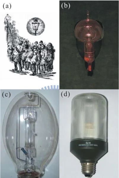
The first commercial technology for lighting was based on natural gas. Gaslight (Fig. 1.1(a)) was introduced by Scottish inventor William Murdoch in the early1790s. At the beginning of the 19th century, luminous combustion of gaseous by-products of coke production was rapidly adopted in towns for indoor domestic, industrial, and public lighting as well as for street lighting. For more than a hundred years, gaslights were strongly improved by the use of mantles soaked with the rare-earth compound thorium oxide, which converted the gas flame’s heat energy and ultraviolet (UV) radiation into visible radiation. Ultimately, however, the gaslights were displaced by incandescent light bulbs first demonstrated in 1879.
Thomas Alva Edison demonstrated the incandescent filament lamp (Fig. 1.1(b)) at 1879 and obtained a patent for a filament lamp.[1] He used a fiber of a particular type of Japanese bamboo as the filament. This was then replaced by osmium, tantalum, and finally, tungsten. Tungsten has the highest melting point and lowest vapor pressure of all metals. The thermal radiation of Tungsten shows a blue shift when compares with black-body radiation, so its luminous efficiency is higher. Tungsten filaments are generally spiraled and protected by glass bulbs which are filled
2
with inert gasses such as Argon and Nitrogen. The luminous efficiency of the 120 V light bulb which radiates at 2400 K is about 8 lm/W, only 7% of the input power can be transferred to visible light.[2]
Discharge in low-pressure gases was investigated intensively and gas discharge lamps were experimented with throughout the 19th century. But not until 1902 did Peter Cooper Hewitt patent the mercury vapor lamp (Fig. 1.1(c)). The lamp was started by mechanical tipping and emitted bluish-green distorted colors. In 1938, General Electric Company (GE) and Westinghouse Electric Corporation put on the market new colored and white lamps that were low-pressure mercury discharge lamps with the inside of the tube coated with a fluorescent powder.[3] The fluorescent lamp uses electricity to excite mercury vapor. The excited mercury atoms produce short-wave ultraviolet light that then causes a phosphor to fluoresce, producing visible light.
In order to make fluorescent light convenient to use, a compact fluorescent lamp (CFL, Fig. 1.1(d)) was designed to fit into most existing light fixtures formerly used for incandescent. CFL was first demonstrated in 1976 by Edward E. Hammer, an engineer of GE. But due to the difficulty of the manufacturing process for coating the interior of the spiral glass tube, GE did not manufacture or sell the device. Other companies began manufacturing and selling the device in 1995. Unlike incandescent lamps, CFLs convert electrical power into useful light more efficiently (~28%). Compared to general service incandescent lamps giving the same amount of visible light, CFLs generally use less power, have a longer rated life (5000-24000 hours depending on the construction), choose able color, and have become the mainstream lighting technology in homes, offices, and public places.[4]
By the end of the 1990s, at the dawn of semiconductor-device lighting, the major part of residential lighting is provided by tungsten incandescent lamps and fluorescent lightings.
3
However, all this is about to change because of the explosive development of solid-state lighting based on high-brightness visible light-emitting diodes (LEDs), which have already found numerous niche applications.
1.2 Light-Emitting Diodes
Light-emitting diodes (LEDs) are a typical p-n junction device used under a forward bias. The basic operating mechanisms are based on the electrical and optical properties of p-n junction and of semiconductor materials. When the diode is forward biased, electrons are able to recombine with holes and energy is released in the form of light. This effect is called electroluminescence. As shown in Fig. 1.2,[5] the wavelength of the light emitted, and therefore its color, depends on the band gap energy of the materials forming the p-n junction. Most commercially available LEDs are made from III-V compound semiconductors. Some II-VI compound semiconductors such as ZnS and ZnSe are used in a few LEDs emitting visible light, through these materials are not used frequently because of the difficulty of p-n junction formation.[6]
1.2.1 Historical Introduction
Electroluminescence was discovered in 1907 by the British experimenter H. J. Round of Marconi Labs, using a crystal of silicon carbide and a cat’s-whisker detector.[7] Russian Oleg Vladimirovich Losev independently created the first LED in the mid 1920s;[8] his research was distributed in Russian, German and British scientific journals, but no practical use was made of the discovery for several decades. LED development began with infrared and red devices made
4
with GaAs. Rubin Braunstein of the Radio Corporation of America first reported on infrared emission from GaAs and other semiconductor alloys in 1955.[9] Braunstein observed infrared emission generated by simple diode structures using GaSb, GaAs, InP, and SiGe alloys at room temperature and at 77 K. Experimenters at Texas Instruments, Bob Biard and Gary Pittman, found in 1961 that GaAs gave off infrared light when electric current was applied. Biard and Pittman were able to establish the priority of their work and received the patent for the infrared light-emitting diode. Nick Holonyak Jr. of the General Electric Company, who is seen as the “father of the light-emitting diode”, developed the first practical visible-spectrum LED in 1962. Since then, related researches went on continually.
In 1972, J. I. Pankove et al. fabricated the first blue LED using III-nitrides materials with a Metal-i-n structure [10]. However, the device performance was limited by the poorly conducting
p-type GaN. The first high-brightness blue LED was demonstrated by Shuji Nakamura of Nichia
Corporation and was based on critical developments in GaN nucleation on sapphire substrates and the demonstration of p-type doping of GaN which were developed by Isamu Akasaki and H. Amano in Nagoya using a low-temperature buffer layer and Low-Energy Electron Beam Interaction (LEEBI) technique, respectively.[11, 12] In 1995, Alberto Barbieri at the Cardiff University Laboratory investigated the efficiency and reliability of high-brightness LEDs and demonstrated a very impressive result by using a transparent contact made of indium tin oxide (ITO) on AlGaInP/GaAs LED. The existence of blue LEDs and high efficiency LEDs quickly led to the development of the first white LED, which employed a Y3Al5O12:Ce, or “YAG”, phosphor coating to mix yellow light with blue to produce light that appears white. Nakamura was awarded the 2006 Millennium Technology Prize for his invention.
5
1.2.2 Advantages of the LED Lighting
LEDs offer numerous benefits due to their mode of operation: (1) Energy Efficiency
LEDs are highly efficient. In traffic signal lights, a strong market for LEDs, a red traffic signal head that contains 196 LEDs draws 10W versus its incandescent counterpart that draws 150W. Various estimates of potential energy savings range from 82% to 93%. With the red signal operating about 50% of the day, the complete traffic signal unit is estimated to save 35-40%. An estimation had been made that replacing incandescent lamps in all of America’s some 260,000 traffic signals (red, green and yellow) could reduce energy consumption by nearly 2.5 billion kWh. At the end of 1997, more than 150,000 signals were retrofitted.
(2) Long Life
Some LEDs are projected to produce a long service life of about 100,000 hours. For this reason LEDs are ideal for hard-to-reach/maintain fixtures such as exit sign lighting and, combined with its durability, pathway lighting. This service life can be affected by the application and environmental factors, including heat and if being overdriven by the power supply.
(3) Range of Colors
LEDs are available in a range of colors, including white light. Fig. 1.3 shows the chromaticity diagram.[13] White light can be produced through color mixing, like red/blue/green, blue/yellow, or green/yellow-green/orange/purple. In addition, through the innovative combination of various-colored LEDs, dramatic color-changing effects can be produced from a single fixture through dynamic activation of various sets of LEDs. Manufacturers such as Color
6
Kinetics offer fixtures that employ this principle. They offer track, theatrical, underwater, outdoor and other fixtures utilizing variable-intensity LEDs that can provide more than 16.7 million colors, including white light. These fixtures can be individually controlled via a PC, DMX controller or proprietary controller to generate effects including fixed color, color washing, cross fading, and random color changing.
(4) Cool Light
In contrast to most light sources, LEDs radiate very little heat in the form of IR that can cause damage to sensitive objects or fabrics. Wasted energy is dispersed as heat through the base of the LED.
(5) Durable
LEDs are highly rugged. They feature no filament that can be damaged due to shock and vibrations. They are subject to heat, however, and being overdriven by the power supply.
(6) Small Size/Design Flexibility
A single LED is very small and produces little light overall. However, this weakness is actually its strength. LEDs can be combined in any shape to produce desired lumen packages as the design goals and economics permit. In addition, LEDs can be considered miniature light fixtures; distribution of light can be controlled by the LEDs’ epoxy lens, simplifying the construction of architectural fixtures designed to utilize LEDs. A controller can be connected to an LED fixture to selectively dim individual LEDs, resulting in the dynamic control of distribution, light output and color. Finally, DC power enables the unit to be easily adaptable to different power supplies.
7
LEDs can very easily be dimmed either by Pulse-width modulation or lowering the forward current.
(8) On/Off Time
LEDs light up very quickly. A typical red indicator LED will achieve full brightness in microseconds. LEDs used in communications devices can have even faster response times.
(9) Cycling
LEDs are ideal for use in applications that are subject to frequent on-off cycling, unlike fluorescent lamps that burn out more quickly when cycled frequently, or HID lamps that require a long time before restarting.
1.2.3 Applications
Many application of LEDs are very diverse but fall into three major categories: Visual signal application where the light goes more or less directly from the LED to the human eye, to convey a message or meaning. Illumination where LED light is reflected from object to give visual response of these objects. Finally LEDs are also used to generate light for measuring and interacting with processes that do not involve the human visual system. These three categories are introduced below:
(1) Signals and Large Displays
The low energy consumption, low maintenance and small size of modern LEDs has led to applications as status indicators and displays on a variety of equipment and installations. Large area LED displays are used as stadium displays and as dynamic decorative displays. Thin,
8
lightweight message displays are used at airports and railway stations, and as destination displays for trains, buses, trams, and ferries.
The single color light is well suited for traffic lights and signals, exit signs, emergency vehicle lighting, ships’ lanterns and LED-based Christmas lights. Red or yellow LEDs are used in indicator and alphanumeric displays in environments where night vision must be retained: aircraft cockpits, submarine and ship bridges, astronomy observatories, and in the field, e.g. night time animal watching and military field use.
Because of their long life and fast switching times, LEDs have been used for automotive high-mounted brake lights and truck and bus brake lights and turn signals for some time. The use of LEDs also has styling advantages because LEDs are capable of forming much thinner lights than incandescent lamps. The significant improvement in the time taken to light up (perhaps 0.5s faster than an incandescent bulb) improves safety by giving drivers more time to react.
Due to the relative cheapness of low output LEDs, they are also used in many temporary applications such as glowsticks and throwies and Lumalive, a photonic textile, artist have also used LEDs for LED art.
(2) Lighting
With the development of high efficiency and high power LEDs, it has become possible to incorporate LEDs in lighting and illumination. Replacement light bulbs have been made as well as dedicated fixtures and LED lamps. LEDs are used as street lights and in other architectural lighting where color changing is used. The mechanical robustness and long lifetime is used in automotive lighting on cars, motorcycles and on bicycle lights.
9
The lack of IR/heat radiation makes LEDs ideal for stage lights using banks of RGB LEDs that can easily change color and decrease heating from traditional stage lighting, as well as medical lighting where IR-radiation can be harmful.
Since LEDs are small, durable and require little power, they are used in hand held devices such as flashlights. LED strobe lights or camera flashes operate at a safe, low voltage, as opposed to the 250 volts commonly found in xenon flashlamp-based lighting. This is particularly applicable to cameras on mobile phones, where space is at a premium and bulky voltage-increasing circuitry is undesirable. LEDs are used for infrared illumination in night vision applications including security cameras. A ring of LEDs around a video camera, aimed forward into a retroreflective background, allows chroma keying in video productions.
LEDs are used for decorative lighting as well. Uses include but are not limited to indoor/outdoor decor, limousines, cargo trailers, conversion vans, cruise ships, RVs, boats, automobiles, and utility trucks. Decorative LED lighting can also come in the form of lighted company signage and step and aisle lighting in theaters and auditoriums.
(3) Non-Visual Applications
Light has many other uses besides for seeing. LEDs are used for some of these applications. The uses fall in three groups: Communication, sensors and light matter interaction.
The light from LEDs can be modulated very fast so they are extensively used in optical fiber and free space optics (FSO) communications. This includes remote controls, such as for TVs and VCRs, where infrared LEDs are often used.
Many sensor systems rely on light as the main medium. LEDs are often ideal as a light source due to the requirements of the sensors. LEDs are used as movement sensors, for example in optical computer mice. Touch sensing: Since LEDs can also be used as photodiodes, they can
10
be used for both photo emission and detection. This could be used in for example a touch-sensing screen that register reflected light from a finger or stylus.
Many materials and biological systems are sensitive to, or dependent on light. Grow lights use LEDs to increase photosynthesis in plants and bacteria and vira can be removed from water and other substances using UV LEDs for sterilization. Other uses are as UV curing devices for some ink and coating applications as well as LED printers.
1.3 III-V Nitride Based LEDs
Creating sources of white light is the ultimate goal of solid-state lighting technology. The most challenging application for LEDs is the replacement of conventional incandescent and probably, even fluorescent lamps. Attempts to up-convert long-wavelength emission of IR LEDs to broader visible spectra were undertaken years ago by Galginaitis and Fenner (1968).[14] Berggren et al. (1994) demonstrated white light-emitting devices made from electroluminescent organic semiconductors.[15] However, practical white LEDs became feasible only after the development of high brightness blue AlInGaN emitters (Nakamura and Fasol 1997).[16] Based on short-wavelength LEDs, white LEDs that exploit the mixture of two or three colors (dichromatic and trichromatic LEDs, respectively) are being developed.
The bandgap energy of AlGaInN varies between 6.2 and 1.95 eV depending on its composition at room temperature, as shown in Fig. 1.2. Therefore, these III-V nitride semiconductors are useful for light emitting devices especially in the short wavelength region. Among AlGaInN system, GaN has been most intensively studied. GaN has bandgap energy of 3.4 eV at room temperature. Previous research on III-V nitrides has paved the way for the realization of high quality crystals of GaN, AlGaN and InGaN, and of p-type conduction in GaN
11
and AlGaN. [17, 18] The beginning of the growth of good quality epilayers was made by Yoshida et al.. [19] They showed in 1983 that if an AlN buffer layer is grown by two step method between the GaN film and the sapphire substrate, the quality of the layers improves. Amano et al. [20] were also the first to obtain p-type conductivity in GaN which used Mg as an accepter. In 1992 van Vechten et al. [21] suggested that Mg-H complexes are formed in the as grown Mg-doped GaN and therefore hydrogen passivates the Mg acceptors. Later it was found that annealing the Mg-doped GaN layers at >750 °C in nitrogen or vacuum also activates the Mg acceptors. [22]
By middle 1990s so much knowledge and experience in technology had accumulated that the progress in designing and fabricating devices became very rapid. High brightness blue LEDs have been fabricated on the basis of these results, and luminous intensities over 1 cd had been achieved in 1994. [23, 24]
1.4 Issues of Nitride Based LEDs
There are three issues of GaN based devices. First, joule heating problem exists which degrades the internal quantum efficiency because of the poor conductivity sapphire substrate. Second, Fresnel loss occurs at the interface of the two different mediums. And third, photons generated from the active layer are trapped inside the device structure because of the total internal reflection.
1.4.1 Joule Heating Problem
12
between the moving particles that form the current (usually, but not always, electrons) and the atomic ions that make up the body of the conductor. Charged particles in an electric circuit are accelerated by an electric field but give up some of their kinetic energy each time they collide with an ion. The increase in the kinetic or vibrational energy of the ions manifests itself as heat and a rise in the temperature of the conductor. Hence energy is transferred from the electrical power supply to the conductor and any materials with which it is in thermal contact.
Due to the lack of native substrates, the GaN-based LEDs must be grown on sapphire substrates, which possess poor thermal conductivity. The sapphire substrate significantly limits the heat dissipation performance of LEDs. The overheating of a LED reduces the quantum yield of light and limits the maximum optical power and service life. The sapphire substrate is classified to a lower thermal-conductivity material, as shown in Table 1.1.[25] In order to achieve better thermal management, the LED epilayer should be transferred to a higher thermal-conductivity substrate, such as Si, Al, or Cu.
1.4.2 Fresnel Reflection
The Fresnel equations, deduced by Augustin Jean Fresnel, describe the behaviour of light when moving between media of differing refractive indices. The reflection of light that the equations predict is known as Fresnel reflection.
When light moves from a medium of a given refractive index n1 into a second medium with refractive index n2, both reflection and refraction of the light may occur. The reflection part is also called “Fresnel loss”. When the light is at near-normal incidence to the interface, the reflection and transmission coefficient are given by:[26]
13 2 1 2 1 2 n n R n n ⎛ − ⎞ = ⎜ + ⎟ ⎝ ⎠ (1.1)
(
1 2)
2 1 2 4 1 n n T R n n = − = + (1.2) When photons pass through GaN (n = 2.5) and air (n = 1) interface, about 18.4% reflection losses will occur because of the large refractive index difference of the two mediums. Inserting an intermediate layer, like indium tin oxide (ITO, n = 2), can moderate this reflection phenomenon. When photons pass through GaN and ITO to air, the reflection losses can thus be reduced to about 12.2%.1.4.3 Total Internal Reflection
Total internal reflection is an optical phenomenon that occurs when a ray of light strikes a medium boundary at an angle larger than a critical angle (the angle of incidence at which light is refracted such that it travels along the boundary) with respect to the normal to the surface. When light crosses a boundary between materials with different refractive indices, the light beam will be partially refracted at the boundary surface, and partially reflected. However, if the angle of incidence is greater than the critical angle, then the light will stop crossing the boundary altogether and instead be totally reflected back internally. This can only occur where light travels from a medium with a higher refractive index to one with a lower refractive index.
Many studies were demonstrated to overcome this problem. In 1993, Schnitzer et al. presented a method of reducing the percentage of total internal reflection light to create light scattering centers in the form of random texturing on the LED’s surface.[27] However, the thickness of the top layer p-GaN cladding is very thin. Consequently, it is not easy to control the
14
dry etching depth and plasma damage to the p-GaN during the dry etching process. Some methods have been used to improve the light extraction efficiency by roughening the top surface[28, 29] or the mesa sidewall [30] of LED. It could also utilize wafer-bonding technology to transfer n-side-up GaN-based LED on Si substrates with a hexagonal “conelike” surface on
n-GaN.[31] Studies described above were focused on a single roughened top surface of
nitride-based LED. In 2006, LED with double roughened surfaces was proposed by Peng et al.[32] They found that double roughened surfaces can give photons higher opportunity to escape form the structure of LEDs than single roughened surface. They also fabricated GaN LEDs with a roughened undoped-GaN surface and a silver mirror on the sapphire substrate.[33] At an injection current of 20 mA, the output power of the roughened LED was further enhanced, which was 1.49 times larger than that of the conventional LED.
1.5 An Overview of the Dissertation
The primary contents of this dissertation are discussing subjects which are relating to the performance enhancement of InGaN-GaN LEDs, including the influence of the mirror location to the light output, the role of the n-bowl structure played in managing the view angle, and the roughening of the ITO window layer.
There are six chapters in this dissertation. In chapter 1, a brief history of the progress of lighting devices is presented. We also make a complete introduction about the LED, which contains history, advantages, applications, development of III-V nitride-based LEDs, and several key issues we might experience while studying it.
In chapter 2, we review the theory and background of this dissertation. The basics of the LED, the Snell’s law, the principles of the reflection loss of light, concave mirror, transmission
15
line model, and wafer bonding are detailed.
In chapter 3, GaN LEDs with double roughened (p-GaN and u-GaN) surfaces and a silver mirror on the sapphire substrate were demonstrated using wafer-bonding and laser lift-off technologies. Effect of the Ag mirror location on the luminance intensity of LEDs was investigated.
In chapter 4, a periodic n-bowl mirror array was introduced into LEDs to improve the LED performance and adjust the view angle. According to L-I characteristics and radiation pattern, this chapter provides the direct evidence that the periodic n-bowl mirror array can not only redirect photons, but also focuses them to the vertical direction of the LED.
In chapter 5, a simple natural lithography process was used to roughen the indium tin oxide (ITO) window layer to improve the InGaN-GaN light-emitting diode (LED) performance. In this lithography process, a photoresist layer was used as a mask for inductively coupled plasma (ICP) dry etching. Transmission line model, SEM and AFM were utilized to understand the contact changing and morphology of the ITO surface after etching. L-I characteristics were also discussed.
Finally, we summarize the overall results of our studies and discuss future works in chapter 6.
16
(a)
(c)
(b)
(d)
Figure 1.1 (a) Illustration of the nightly illumination of a gaslight with a thorium
oxide–soaked mantle. (b) Original carbon-filament bulb from Thomas Edison. (c)
A closeup of a 175W mercury vapor lamp. (d) An early compact fluorescent lamp.
17
Figure 1.2 Bandgap energy of various materials for visible emission devices as a
function of their lattice constant.[5]
18
Figure 1.3 Chromaticity diagram. White light can be produced through color
mixing, like red/blue/green, blue/yellow, or green/yellow-green/orange/purple.[13]
19
20
CHAPTER 2
BACKGROUND AND THEORY
2.1 Basics of LEDs
Conventional lamps rely on either incandescence or discharge in gases. Both phenomena are associated with large energy losses that are essentially inherent because of the high temperatures and large Stokes shifts involved. LEDs offer an alternative way of light generation. Spontaneous light emission in LEDs is due to radiative recombination of excess electrons and holes. Excess electrons and holes are produced by current injection with small energy losses. Subsequent radiative recombination of the injected carriers may attain quantum yields close to unity. This phenomenon, called electroluminescence, is the energy-saving promise of this generation. In this section we deal with the basics of LEDs which include device configuration, recombination of electrons and holes, injection in a p-n junction, electroluminescent structure, and LED performance.
2.1.1 Device Configuration
The schematic of a typical surface-emitting LED is shown in Fig. 2.1. Like a normal diode, the LED consists of a chip of semiconducting material doped with impurities to create a p-n junction. The doped materials are known as the p- and n-confinement layer. Electrodes that usually contain Au and Al are placed on the top and the bottom of the structure. To make connection between the power and the chip, wire bonding is often used on the top electrode. The
21
size of it must be precisely controlled. If it is too large or too small, hindering effect and current crowing will occur to decrease the luminance efficiency, respectively.
LEDs are usually built on an n-type substrate and the structure is grown by epitaxial techniques with an electrode attached to the p-type layer deposited on its surface. p-Type substrates, while less common, occur as well. Many commercial LEDs, especially GaN/InGaN, also use sapphire substrate. Lattice matching is an important issue for epitaxy. Typically, films of different materials grown on the substrate are chosen to match the lattice constant of the substrate material to minimize film stress.
Most materials used for LED production have very high refractive indices. This means that much light will be reflected back into the material at the material/air surface interface. Therefore Light extraction in LEDs is also an important aspect of LED production, subject to much research and development.
2.1.2 Recombination of Electrons and Holes
Carrier recombination result from interaction between electrons and other carriers, either with the lattice of the material, or with optical photons. As the electron moves from one energy band to another, its gained or lost energy must take some other form, like heat and photon. Excess carriers can recombine both radiatively and nonradiatively. Competition between radiative and nonradiative recombination processes determines the internal quantum efficiency of an LED. As shown in Fig. 2.2,[1] an intrinsic mechanism of radiative recombination is band-to-band transitions, in which an electron-hole pair recombines, emitting a photon. Radiative annihilation of excitons is the second intrinsic mechanism of light emission. In some alloys used for the fabrication of LEDs (like InGaN), the nonuniformity of the spatial distribution of constituents
22
may cause considerable fluctuations of the band potential. Carriers that are localized at such fluctuations recombine radiatively with large probability. This is the third intrinsic mechanism of radiative recombination.
Other mechanisms of radiative recombination are link to impurities caused by defects and/or by intentional or unintentional doping. The impurity levels in the bandgap trap free carriers that may contribute to photon emission. For instance, a radiative transition between the conduction band and an acceptor state or between a donor state and the valence band might occur. Also, electrons trapped at donor states can recombine radiatively with holes trapped at acceptor states. Finally, a trapped carrier can form an excitonic complex with a carrier of different type. In many semiconductors, radiative annihilation of bound excitons is the main emission mechanism at low temperatures and at low densities of excess carriers.
2.1.3 Injection in a p-n Junction
The basic element of an LED is a semiconductor electroluminescent structure that comprises, at least, a region of radiative recombination and regions of different conductivity type (p and n) that supply the recombining carriers. In the simplest design, the structure relies on a junction between a p-type semiconductor and an n-type semiconductor of the same kind with one or both conductivity regions employed as the radiative-recombination region or regions. Figure 2.3 depicts a band diagram of a p-n homojunction. Under zero bias, the majority electrons from the
n-region diffuse into the p-region and the majority holes diffuse in the opposite direction. This
process creates depleted regions on both sides of the interface. The space charge of the depleted regions creates an internal electric field that counteracts the diffusion. In equilibrium, when the potential barrier is somewhat smaller than the bandgap energy, the diffusion current is
23
counterbalanced by the reverse current of minority carriers that drift in this internal electric field. When a voltage V is applied in the forward direction, the reverse currents of the minority carriers change negligibly. Meanwhile, the barrier for majority carriers decreases by qV. Consequently, the majority-carrier diffusion current increases. Enhancement of the diffusion due to the electric field results in an excess density of minority carriers on both sides of the junction. The injected carriers recombine both radiatively and nonradiatively.
2.1.4 Electroluminescent Structure
Conventional p-n diodes utilize doping profiles to control carrier injection. The potential barriers for electrons and holes are created by the charges of ionized donors and acceptors in the depletion region near the boundary between the n- and p-type semiconductors. LEDs based on
p-n homojunctions have important shortcoming that limits their application in solid-state lighting.
The light generated in the active region is reabsorbed, to a considerable extent, in the conductive regions. This reduces the light-extraction efficiency.
Thinning the active layer is the way to further increase the rate of radiative recombination and reduce the reabsorption. In addition, using very thin active layers enables one to overcome some lattice-matching problems, since such layers are able to conform to the thick confining layers without defect generation. Such double heterostructures are called quantum well (QW) structures.[2] Single quantum wells (SQWs) and multiple quantum wells (MQWs) offer the most versatile structures for high-brightness LEDs.
Fig. 2.4 depicts a band diagram of QW structure composed of a thin layer of a semiconductor with the bandgap energy Eg2 sandwiched between thick cladding layers of a
24
particles, which were originally free to move in three dimensions, to two dimensions, forcing them to occupy a planar region. The effects of quantum confinement take place when the quantum well thickness becomes comparable at the de Broglie wavelength of the carriers, leading to energy levels called “energy subbands”, i.e., the carriers can only have discrete energy values. Light-emitting structures based on QWs require optimization of the injection efficiency. The drawback is that in materials used for LED fabrication, electron mobility is very high and electrons can leak into the p-type cladding layer without being captured by the QW states. The leakage is less probable for holes, which have much less mobility. Usually, an electron blocking layer (EBL) made of a wider-gap p-material is introduced between the QW and the p-conductive layer to prevent leakage of electrons into the p-type conductive layer and thus to improve injection efficiency.[3]
2.1.5 Efficiency
An injection-electroluminescence device is characterized by its radiant efficiency (also called wall-plug efficiency)
e ext f
η =η ×η (2.1)
where ηext is the external quantum efficiency and ηf is the feeding efficiency. Feeding efficiency is
the ratio of the mean energy of the photons emitted and the total energy that an electron-hole pair acquires from the power source when passing through the LED:
f
h qV
ν
η = (2.2)
where h is the Planck’s constant (4.14× 10⁻¹⁵ eV·sec), ν is the mean frequency of photons, V is the forward voltage drop across the LED and q is the elementary charge (1.60×10⁻¹⁹ C).
25
External quantum efficiency (EQE) is the ratio of the number of photons emitted and the number of electrons passed through the LED. Explicitly, it is the product of the injection efficiency, ηinj; radiative efficiency, ηrad; and optical efficiency, ηopt:
ext inj rad opt
P h I q ν η = =η ×η ×η (2.3)
where P is the total power emitted out of the LED, ν is the frequency of the photon, and I is the injection current. Injection efficiency is the fraction of the electrons passed through the LED that are injected into the active region, where radiative recombination takes place:
n inj I I η = (2.4) 0 exp 1 n n B qV I I k T ⎡ ⎛ ⎞ ⎤ = ⎢ ⎜ ⎟− ⎥ ⎝ ⎠ ⎣ ⎦ (2.5)
where In is the injection current introduced in the p-region, In0 is the reverse current for minority
electrons, kB is the Boltzmann constant, and T is the temperature of the crystal. Radiative
efficiency (also called internal quantum efficiency, IQE) is the ratio of the number of electron-hole pairs that recombined radiatively to the total number of pairs that recombined in the active region: 1 1 rad r r nr τ η τ τ τ = = + (2.6)
here τ is the overall lifetime of the carriers, τr and τnr are the lifetimes of the carriers which
recombine radiatively and nonradiatively, respectively. Finally, optical efficiency (also called light-extraction efficiency) is the fraction of the photons generated that escape from the device.
26
2.2 Snell’s Law
Snell’s law is used to determine the direction of light rays through refractive media with varying indices of refraction.[4] The indices of refraction of the media, labeled n1, n2 and so on, are used to represent the factor by which a light ray’s speed decreases when traveling through a refractive medium, such as glass or water, as opposed to its velocity in a vacuum.
As light passes the border between media, depending upon the relative refractive indices of the two media, the light will either be refracted to a lesser angle, or a greater one. These angles are measured with respect to the normal line, represented perpendicular to the boundary. In the case of light traveling from air into water, light would be refracted towards the normal line, because the light is slowed down in water; light traveling from water to air would refract away from the normal line. Refraction between two surfaces is also referred to as reversible because if all conditions were identical, the angles would be the same for light propagating in the opposite direction.
Snell’s law is generally true only for isotropic or specular media (such as glass). In anisotropic media such as some crystals, birefringence may split the refracted ray into two rays, the ordinary or o-ray which follows Snell’s law, and the other extraordinary or e-ray which may not be co-planar with the incident ray.
Named after Dutch mathematician Willebrord Snellius, one of its discoverers, Snell’s law states that the ratio of the sines of the angles of incidence and refraction is equivalent to the ratio of velocities in the two media, or equivalent to the opposite ratio of the indices of refraction:
1 1 2 2 2 1 sin sin v n v n θ θ = = (2.7)
27
Snell’s law follows from Fermat’s principle of least time, which in turn follows from the propagation of light as waves.
2.3 Reflection Losses of Light
When light travels from one medium to another, two types of reflection losses will occur because of the indices difference between two mediums. One is total internal reflection and the other is Fresnel loss.
2.3.1 Total Internal Reflection
When light travels from a medium with a higher refractive index to one with a lower refractive index, Snell’s law seems to require in some cases (whenever the angle of incidence is large enough) that the sine of the angle of refraction be greater than one. This of course is impossible, and the light in such cases is completely reflected by the boundary, a phenomenon known as total internal reflection.[5]
Total internal reflection is an optical phenomenon that occurs when a ray of light strikes a medium boundary at an angle larger than a particular critical angle with respect to the normal to the surface. If the refractive index is lower on the other side of the boundary, no light can pass through and all of the light is reflected. The largest possible angle of incidence which still results in a refracted ray is called the critical angle; in this case the refracted ray travels along the boundary between the two media.
The critical angle is the angle of incidence above which total internal reflection occurs. The angle of incidence is measured with respect to the normal at the refractive boundary. The critical
28
angle θC is given by:
1 2 1 sin C n n θ = − ⎛ ⎞ ⎜ ⎟ ⎝ ⎠ (2.8)
where n2 is the refractive index of the less optically dense medium, and n1 is the refractive index of the more optically dense medium. Because of the critical angle, there is a cone-like region formed near the surface when the light travels between these two mediums. Only the light within the cone can be extracted, the light outside the cone will experience total internal reflection until it is absorbed.
2.3.2 Fresnel Loss
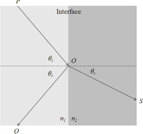
When light moves from a medium of a given refractive index n1 into a second medium with refractive index n2, both reflection and refraction of the light may occur.[6] In Fig. 2.5, an incident light ray PO strikes at point O the interface between two media of refractive indexes n1 and n2. Part of the ray is reflected as ray OQ and part refracted as ray OS. The angles that the incident, reflected and refracted rays make to the normal of the interface are given as θi, θr and θt,
respectively. The relationship between these angles is given by the law of reflection and Snell's law.
The fraction of the incident power that is reflected from the interface is given by the reflectance R, which is also called the Fresnel losses, and the fraction that is refracted is given by the transmittance T.
The calculations of R and T depend on polarisation of the incident ray. If the light is
polarised with the electric field of the light perpendicular to the plane of the diagram above (s-polarised), the reflection coefficient is given by:
29
(
)
(
)
2 2 1 2 2 1 2 2 1 2 2 1 2 1 1 2 2 cos 1 sin sin cos cossin cos cos
cos 1 sin i i t i i t S t i i t i i n n n n n n R n n n n n n θ θ θ θ θ θ θ θ θ θ θ θ ⎡ ⎛ ⎞ ⎤ ⎢ − − ⎜ ⎟ ⎥ ⎢ ⎥ ⎡ − ⎤ ⎛ − ⎞ ⎝ ⎠ =⎢ ⎥ =⎜ ⎟ = ⎢ ⎥ + ⎝ + ⎠ ⎢ ⎥ ⎣ ⎦ ⎛ ⎞ + − ⎢ ⎜ ⎟ ⎥ ⎢ ⎝ ⎠ ⎥ ⎣ ⎦ (2.9)
where θt can be derived from θi by Snell's law and is simplified using trigonometric identities.
If the incident light is polarised in the plane of the diagram (p-polarised), the R is given by:
(
)
(
)
2 2 1 2 2 1 2 2 1 2 2 1 2 1 1 2 2 1 sin cos tan cos costan cos cos
1 sin cos i i t i t i P t i t i i i n n n n n n R n n n n n n θ θ θ θ θ θ θ θ θ θ θ θ ⎡ ⎛ ⎞ ⎤ ⎢ −⎜ ⎟ − ⎥ ⎢ ⎥ ⎡ − ⎤ ⎛ − ⎞ ⎝ ⎠ =⎢ + ⎥ =⎜ + ⎟ = ⎢ ⎥ ⎝ ⎠ ⎢ ⎥ ⎣ ⎦ ⎛ ⎞ − + ⎢ ⎜ ⎟ ⎥ ⎢ ⎝ ⎠ ⎥ ⎣ ⎦ (2.10)
The transmission coefficient in each case is given by Ts = 1 − Rs and Tp = 1 − Rp.
When the light is at near-normal incidence to the interface (θi ≈ θt ≈ 0), the reflection and
transmission coefficient are given by:
2 1 2 1 2 S P n n R R R n n ⎛ − ⎞ = = = ⎜ ⎟ + ⎝ ⎠ (2.11)
(
1 2)
2 1 2 4 1 S R n n T T T R n n = = = − = + (2.12)2.4 Concave Mirror
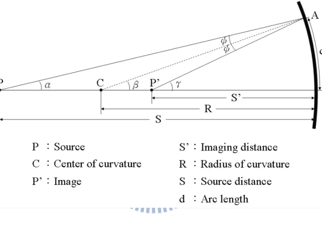
A concave mirror, or converging mirror, has a reflecting surface that bulges inward (away from the incident light). Concave mirrors reflect light inward to one focal point, therefore they are used to focus light. Unlike convex mirrors, concave mirrors show different image types depending on the distance between the object and the mirror.
30
These mirrors are called “converging” because they tend to collect light that falls on them, refocusing parallel incoming rays toward a focus. This is because the light is reflected at different angles, since the normal to the surface differs with each spot on the mirror. In this study, we used concave mirror to redirect photons to the vertical direction of the LED which generated from the MQW and originally emitted downward.
As shown in Fig. 2.6, if light source is placed at the left side of the curvature center of the concave mirror, there will be an image formed at the right side of the curvature center. From the
PAC
Δ and ΔPAP', we can easily have the relation as follow 2
α γ+ = β (2.13) If the paraxial ray is considering, ∠ , α ∠ and β ∠ will be very small and hence γ
d S α ≈ , d R β ≈ , and ' d S γ ≈ (2.14) From (2.13) and (2.14), we can receive
1 1 2 '
S+S = R (2.15)
In order to collect photons from the vertical direction of the LED (S'= ∞ ), MQW must be placed at the focal plane (focal length = f) of the concave mirror. From (2.15), we can derive
2
R f = and reform the relation into
1 1 2 1 '
S+S = R= f (2.16)
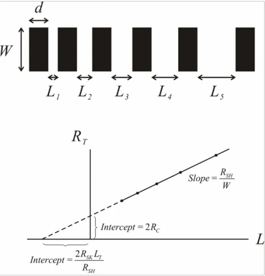
2.5 Transmission Line Model (TLM)
31
method for determining the specific contact resistance (ρC) for planar ohmic contacts.[7]
Shockley proposed an experiment in which the total resistance RT between any two contacts (of
length d and width W) separated by a distance L could be measured and plotted as a function of L. As shown in Fig. 2.7, the total resistance (RT) between any two contacts is given by:
2 SH T C R L R R W = + (2.17)
where RSH is the sheet resistance of the semiconductor layer outside the contact region. The
contact resistance RC can be shown as:
coth SK T C T R L d R W L ⎛ ⎞ = ⎜ ⎟ ⎝ ⎠ (2.18) C T SK L R ρ = (2.19)
where RSK is the modified sheet resistance under the contact and LT is the transfer length. When d
>> LT, coth ~ 1 T d L ⎛ ⎞ ⎜ ⎟
⎝ ⎠ and equation (2.17) can be transferred to 2 SK T SH T R L R L R W W = + (2.20)
Using ordinary least squares (OLS), the linear relationship between RT and L can be exactly
performed and the variables can be defined by the intercepts and the slope as follow:
Intercept of the axis RT =2RC (2.21)
Intercept of the axis L 2 SK T SH R L R = (2.22) Slope m RSH W = (2.23)
32
2.6 Wafer Bonding
To join two different materials, wafer bonding technique shows a benefit when compares with the ordinary growth technique because defects can be confined at the interface. Wafer bonding has two stages: first is wafer contacting and second is wafer binding. Surfaces of these two materials must be smooth while contact with each other. Weak forces form between them which appear in the following three types: (1) van der Waals force, (2) Capillary action, and (3) electrostatic force, as shown in Fig. 2.8.[8]
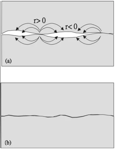
Although weak forces will form at the contact process, it still needs a high temperature annealing and a uniaxial pressure to construct high strength bonds between the two materials in binding process. By using a special treatment to the wafer surface, wafer binding can also be proceeded at low temperature. The weak bonds can finally be transferred to covalent bonds. The exterior layers of all the solid state materials exist in non-equilibrium and reconstructed states. As we know, the property of this exterior layer is different from the inside which has higher energy. From the thermaldynamics point of view, the surface free energy is positive and the volume free energy is negative. In order to reduce the total energy, two bound surfaces tend to fuse together and eliminate the bonding interface. The driving force to the interface elimination is offered by the difference of the surface curvature. The following sentence expresses the relationship between the change of the free energy G and the radius of the curvature r.[9]
2 8 2 4 dG dG dr dG dA dr r dV dr dV dA dr dV r r π γ γ π = = = = (2.24)
From this equation, we can easily see that the driving force is apparently inverse proportion to the radius of the surface curvature. When two wafers bound together, the micro-undulations lead to the diffusion of the atoms. As shown in Fig. 2.9, atoms at the sites with positive curvature (r > 0)
33
move to the negative ones (r < 0) using surface diffusion and lattice diffusion. When the binding completes, covalent bonds will form at the interface which are much stronger than the original contact force.
34
35
Figure 2.2 Intrinsic radiative transitions in semiconductors. (a) Band-to-band
transitions; (b) free-exciton annihilation; (c) recombination of exciton localized at
band-potential fluctuations.[1]
36
Figure 2.3 Band structure near a semiconductor p-n homojunction: (a) under zero
bias; (b) under forward bias.[1]
37
38
Figure 2.5 Behavior of light when traveling between two different mediums. Both
reflection and refraction occur.
39
40
Figure 2.7 (a) Schematic illustration of the TLM patterns. (b) Plot of total contact
as a function of L to obtain transfer length and contact resistance values.
41
42
Figure 2.9 (a) Diffusion occurred because of the difference of surface curvature.
(b) Interface after annealing.
43
CHAPTER 3
EFFECT OF THE SILVER MIRROR LOCATION ON THE
LUMINANCE INTENSITY OF DOUBLE-ROUGHENED GAN
LIGHT-EMITTING DIODES
3.1 Introduction
Recently, epitaxial growth techniques have significantly improved the luminance intensity of light-emitting diode (LED). GaN-based LEDs are attractive devices for use in a variety of applications including traffic signals, full-color displays, back lighting in liquid-crystal displays, and mini projectors.[1,2] However, the light extraction efficiency of GaN-based LEDs is limited by the large difference in refractive index between the GaN film and the surrounding air. According to the Snell's law, light traveling from GaN to air travels only within a critical angle of 23°. The light reaching the surface beyond the critical angle will experience total internal reflection that will continue to be reflected within the LED until it is absorbed. Some methods have been used to reduce the percentage of total internal light reflection by roughening the top
p-GaN surface.[3-8] It could also utilize wafer-bonding and laser lift-off technologies to transfer
the random texturing of undoped-GaN (u-GaN) surface onto Si substrates,[8-10] or bond various mirror systems between the GaN LED structures and the substrate.[9] In this study, GaN LEDs with double roughened (p-GaN and u-GaN) surfaces and a silver (Ag) mirror on the sapphire substrate were successfully fabricated using wafer-bonding and laser lift-off technologies. Effect of the Ag mirror location on the luminance intensity of LEDs was investigated.
44
3.2 Experiments
3.2.1 Illustration and abbreviation of LEDs
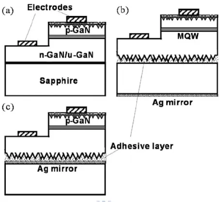
Three kinds of LEDs were used in this study. As illustrated in Fig. 3.1, samples designated as “PR-LED” were LEDs with roughened p-GaN surface. Samples designated as “DRM-LED” and “DRSM-LED” were LEDs with double roughened (p-GaN and u-GaN) surfaces and an Ag mirror system either between the GaN LED structure and sapphire substrate or on the backside of sapphire substrate.
3.2.2 Crystal growth and device process of PR-LED
The devices processes for PR-LED, DRM-LED and DRSM-LED were the same and were shown in Fig. 3.2. The InGaN-GaN films were grown by low-pressure metal organic chemical vapor deposition (MOCVD) on a sapphire substrate. The LED structures were consisted of a 5-nm-thick Si-doped n+-InGaN tunnel contact structure, a 0.4-µm-thick Mg-doped GaN layer, an InGaN-GaN multiple quantum well (MQW), a 2-µm-thick Si-doped GaN layer, a 2-µm-thick
u-GaN layer film and a buffer layer on a sapphire substrate. The Si-doped n+-InGaN layer was used to form the ohmic contact between ITO and p-GaN.[11] The device mesa with a chip size of 300×300 µm2 was then defined by an inductively coupled plasma (ICP) to remove Mg-doped GaN layer and MQW until the Si-doped GaN layer was exposed. Then, the indium tin oxide (ITO) layer was deposited on the n+- InGaN layer to form a p-side contact layer and a current spreading layer. The Cr/Au layer was deposited onto the ITO layer to form the p-side and n-side electrodes. The roughened p-type GaN surfaces of PR-LED were formed by lowering the epitaxy growth temperature of the p-type GaN layer.[7,8]
![Figure 1.2 Bandgap energy of various materials for visible emission devices as a function of their lattice constant.[5]](https://thumb-ap.123doks.com/thumbv2/9libinfo/8717142.200316/31.892.180.747.322.819/figure-bandgap-various-materials-visible-emission-function-constant.webp)
![Figure 2.2 Intrinsic radiative transitions in semiconductors. (a) Band-to-band transitions; (b) free-exciton annihilation; (c) recombination of exciton localized at band-potential fluctuations.[1]](https://thumb-ap.123doks.com/thumbv2/9libinfo/8717142.200316/49.892.142.784.346.704/intrinsic-radiative-transitions-semiconductors-transitions-annihilation-recombination-fluctuations.webp)
![Figure 2.8 Three situations when two wafers contact with each other.[8]](https://thumb-ap.123doks.com/thumbv2/9libinfo/8717142.200316/55.892.200.721.360.848/figure-situations-wafers-contact.webp)