國 立 交 通 大 學
光 電 工 程 研 究 所
碩士論文
非極性"a"平面氧化鋅多重量子井結構之光
學特性
Optical Characteristics of a-plane
ZnO/Zn
0.8
Mg
0.2
O MQWs grown by Pulsed
Laser Deposition
研
研
究
究
生
生
:
:
卓
卓
立
立
夫
夫
..指
指
導
導
教
教
授
授
:
:
郭
郭
浩
浩
中
中
教
教
授
授
盧
盧
廷
廷
昌
昌
教
教
授
授
非極性"a"平面氧化鋅多重量子井結構之光學特性
Optical Characteristics of a-plane ZnO/Zn
0.8Mg
0.2O MQWs
grown by Pulsed Laser Deposition
研究生:卓立夫 Student: Li. Fu. Zhuo
指導教授:郭浩中 教授 Advisor: Prof. Hao-chung Kuo
盧廷昌 教授 Prof. Tien-chang Lu
國 立 交 通 大 學 電機資訊學院
光電工程研究所
碩 士 論 文
A Thesis
Submitted to Institute of Electro-Optical Engineering College of Electrical Engineering and Computer Science
National Chiao Tung University in Partial Fulfillment of the Requirements
for the Degree of Master
In
Electro-Optical Engineering
July 2009
Hsinchu, Taiwan, Republic of China
非極性"a"平面氧化鋅多重量子井結構之光學特性
研究生:卓立夫 指導教授:郭浩中 教授 盧廷昌 教授國立交通大學光電工程研究所
摘要
在本篇論文中,我們利用脈衝雷射蒸鍍製程技術成長不同的非極性"a"平面 氧化鋅/氧化鋅鎂多重量子井作為研究對象。在特性分析中,包含了結構與光學 特性上的相關研究。在發光特性方面,所利用的是光激發螢光光譜(PL),以及吸 收光譜(absorption spectra)技術進行樣品的光學特性分析,結構及相關成分的 研究包含了穿透式電子顯微鏡圖像、能量散佈光譜、選區繞射…。 在低溫 PL 可以觀察到比較薄的量子井有較高的量子侷限效應,同時在變功 率的 PL 實驗中,發現樣品的發光波長並不隨者雷射功率增加而改變,意味者非極 性面成長的氧化鋅多重量子井確實有效的抑制了 QCSE 的效應。從變溫 PL 的光譜 變化顯示激子有效的侷限在量子井中以及藉由變溫 PL 的曲線擬合的結果可以得 到 激 子 的 束 縛 能 有 效 的 提 高 。 成 長 非 極 性 結 構 的 另 一 優 勢 在 於 極 化 發 光 (polarized light emission)的價值,我們所測得的發光極化率大約在 93%左右 (@20K)。偏振的吸收光譜解析出了價電帶的能帶位置,而第一個價電帶和第二個 價電帶的能量差正是使得氧化鋅的多重量子井有高極化率的主因。 將雷射聚焦到微米等級,並且使用 YVO4 脈衝雷射去光激發我們的樣品可以 觀察到氧化鋅非線性光學的發光現象。在極高的雷射能量密度下光激發,觀察到 了電子電洞所形成離子團的發光特性,並且出現了 random lasing 的特殊現象, 此種不需要反射鏡即可產生半高寬小於 0.37nm 的光源,值得未來更進一步的開 發成電激發的光電雷射元件。
Optical Characteristics of a-plane ZnO/Zn0.8Mg0.2O MQWs grown by Pulsed Laser Deposition
Student: Li Fu Zhuo Advisors: Prof. Hao-chung Kuo Prof. Tien-chang Lu
Institute of Electro-Optical Engineering, National Chiao Tung University
Abstract
In this thesis, a-plane ZnO/ZnMgO multiple quantum wells were grown on r-plane sapphire by pulsed laser deposition for investigation. We utilized several methods including photoluminescence (PL), polarized absorption spectra, and micro photoluminescence (μ-PL) to investigate the optical characteristics of our samples. Energy dispersive spectrometer revealed the magnesium concentration of barrier layer is 20%. Transmission electronic microscopy was further carried out to determine the growth direction of MQWs along [11-20] and the barrier and well thicknesses.
The low temperature PL experiments revealed that the larger quantum confinement in thinner quantum well. Meanwhile, the power dependent PL measurement indicated no apparent emission peak shift for all samples due to no built-in electric field in a-plane MQWs. Moreover, the temperature dependent PL reveals that excitons were confined well in MQWs. From the fitting result of activation energy, the exciton binding energy was further enhanced by quantum well.
structure was observed. Larger △E (E2-E1) was the main reason which induced high polarization ratio. Further, we demonstrated the random lasing behavior of a-plane
ZnO/ZnMgO MQWs. At high excitation intensity (~55.7MWcm-2), many sharp peaks
emerge on the spectra. The FWHM of each individual peaks was about 0.37nm and the mode spacing was about 0.65nm. From the equation we had calculated the exciton binding energy is around 66meV which is closed to the activation energy. We attributed this lasing behavior from the forming of electron-hole plasma and the
threshold was about 47.33MWcm-2. For constant pump intensity of 113 MWcm-2,
larger excitaition area produces EHP lasing behavior easier. This is also a characteristic behavior in random lasing system.
Acknowledgement
碩士班的兩年實在過的非常的快,沒想到竟然輪到我畢業了,回頭看看這兩 年,真得是充滿者歡笑與淚水阿!!!首先,一定要先感謝我們實驗室的三位老師: 王老師,郭老師,盧老師。王老師每次爽朗的笑容總是讓大家歡樂許多,郭老師 對我們的要求,讓我們知道碩士班的學生應該要做到什麼樣的水準,盧老師對實 驗的挑剔,讓我知道做實驗以及分析數據應該要保持什麼樣的態度,相信未來三 位老師們ㄧ定能帶領實驗室為台灣做出更多更好的研究成果。 謝謝宗憲學長對我的指導,學長的遠見以及對實驗方向的獨特嗅覺,使得我不 用浪費很多時間,而能很有效的解決問題。除了實驗方面學長對於我做人處事方 面也指導許多,讓我做人更圓融,更懂得怎麼看人。 第二個幫助我最多的人就是俊榮學長,你雖然給我的意見不多,但都是很關鍵 的幾個癥結。平常俊榮對學弟妹的照顧實在是揪甘心ㄟ!!!。小閔學長做事非常細 心,我們總是一起煩惱小咪要報告什麼,一起討論一些問題,不過我要先你一步 走了,保重阿。 玫君,你常常削水果請我們吃,碩一的時候我們一起完成了很多困難的作業, 希望我們兩個都能減肥成功,小楊,雖然我不愛喝酒不愛吃宵夜,不過我還是很 樂意陪你聊天的,你的用語實在讓我們津津樂道阿!阿綱、小馬、智凱、小柯、 政暐、QQ,很開心跟你們做同學,祝你們都順順利利的以後常聯絡阿。 實驗室的學弟妹們也幫助我很多,福吉雖然我很喜歡開你玩笑,不過你知道我 是打打嘴砲的,獸黃你太沒有個性了,不要再當爛好人了,硬起來吧!阿淇仔你 做事看起來很大膽其實你的內心是很纖細的,以後多多照顧獸黃吧,大衛平常找 你打球,你都非常阿莎力,真得是我很好的打球咖。 最後感謝謝老師實驗室的學長們,尤其是小郭學長,真得給了我很多的幫助, 要感謝的人實在太多了,不如就謝天吧,祝我的朋友們都順順利利的,大家加油。Content
Abstract (in Chinese)……….………..…………..i
Abstract (in English )………..……….ii
Acknowledgement………...………....iv
Content………...……….…...v
List of Figures...vii
Chapter 1 Introduction and Motivation……….1
1.1 Introduction to opto-electronic material………...1
1.2 Material characteristics of zinc oxide………...3
1.3 Fabrication of nanostructure materials……….6
1.4 Motivation of a-plane ZnO / ZnMgO MQWs structure………...7
Chapter 2 Properties of nonpolar multiple quantum wells (MQWs)
structure………...11
2.1 Quantum confinement effect in semiconductor nanostructure………...11
2.2 The basic concept of nonpolar nanostructure……….13
2.3 In-plane light polarization effect in nonpolar nanostructure………..15
Chapter 3 Sample growth and experiment apparatus………18
3-1 Growth mechanism of ZnO/ZnMgO MQWs using pulsed laser deposition…….18
3-2 Transmission Electron Microscope, Energy Dispersive X-ray Spectroscopy (EDS) and Selected Area Electron Diffraction(SAED)………..21
3-3 Photoluminescence………27
3-4 Absorption………..28
MQWs………..……37
4-1 Samples preparation and growth………37
4-2 Photoluminescence spectra of a-plane ZnO/ ZnMgO MQWs………...39
4-3 Nonpolar characteristics of a-plane a-plane ZnO/ ZnMgO MQWs………...40
4-4 The localization effect of a-plane ZnO/ ZnMgO MQWs………...42
4.5 In-plane polarization effect of a-plane ZnO/ ZnMgO MQWs emission…………45
4.5.1 In-plane polarization effect of a-plane ZnO/ ZnMgO MQWs emission…….45
4.5.2 Absorption spectra of a-plane ZnO/ZnMgO multiple quantum wells……….46
4.6Conclusion………...47
Chapter 5 Random lasing behavior in a-plane ZnO/ZnMgO
MQWs………..60
5.1 Introduction………60
5.2 Optical pumping of a-plane ZnO/ ZnMgO MQWs………63
5.4 Conclusion………..66
Chapter 6 Conclusion and future work………73
6.1 Conclusion………..73
6.2 Future work………74
List of Figures
Fig. 1.1.1 Band bending resulted from QCSE in polar III-nitride quantum well with different thicknesses……….………...9 Fig 1.2.1 Crystal structure of Zinc oxide………...………9 Fig 1.3.1 Dimension of nanostructure and corresponding density of state………….9 Fig. 1.3.2 The carrier behavior in three dimensional confinement structure………...10 Fig. 2.2.1 The planar relation and orientation in hexagonal crystal structure…..……17 Fig 2.2.2 A schematic energy band diagram of (a) nonpolar quantum well and (b) polar quantum well under QCSE………...…..17 Fig 3.1.1 PLD system………...33 Fig. 3.2.1 (a) Ray diagram for viewing the image and (b) the diffraction pattern of the sample……….……..33 Fig 3.3.1 The schematic diagram of photoluminescence setup………34 Fig 3.4.1 Different types of optical absorption phenomena; (1) transitions of high-lying bands, (2) excitons, (3) fundamental absorption (4) impurity absorption, (5) free-carrier absorption and (6) Reststrahlen absorption.………..………34
Fig 3.4.2 The momentum-conserving transitions are allowed……….35
Fig 3.4.3 The left diagram shows the perturbation of the band edges by Coulomb interaction with inhomogeneously distributed impurities. This leads to the formation of tails of states shown on the right side. The dashed lines show the distribution of states in the unperturbed case.………...35
Figure 3.4.4 The typical absorption edge of a direct semiconductor.………..36 Fig 3.4.5 Absorption system………...……….36 Fig. 4.1.1 TEM measurement results of the five pairs ZnO/ZnMgO MQWs (a) bright field (b) dark field………....…...49 Fig. 4.1.2 TEM measurement results of the ten pairs ZnO/ZnMgO MQWs (a) bright field (b) dark field………...49 Fig. 4.1.3 Selected area Electron diffraction (a) Electron beam direction from c-axis (b) Electron beam direction from m-axis……….50 Fig.4.2.1 PL measurement results of all samples at 20K...50 Fig 4.2.2 (a) Simulation & PL spectrum of five pairs ZnO/ZnMgO MQWs (@300K)……….…….51 Fig 4.2.2 (b) Simulation & PL spectrum of ten pairs ZnO/ZnMgO MQWs (@300K)………...51 Fig 4.3.1 (a) Power-dependent PL spectra for five pairs ZnO/ZnMgO MQWs…..52 Fig 4.3.1 (b) Power-dependent PL spectra for ten pairs ZnO/ZnMgO MQWs.…..52 Fig4.3.2 (a) Power-dependent PL fitting result for five pairs ZnO/ZnMgO MQWs………...53 Fig4.3.2 (b) Power-dependent PL fitting result for ten pairs ZnO/ZnMgO MQWs………..53 Fig 4.4.1 (a) The evolution of PL spectra as a function of temperature for the five pairs ZnO/ZnMgO MQWs………..…54 Fig 4.4.1 (b) The evolution of PL spectra as a function of temperature for the ten pairs
Fig 4.4.2 (a) The peak shift of five pairs ZnO MQW emission over the investigation
temperature range……….55
Fig 4.4.2 (a) The peak shift of ten pairs ZnO MQW emission over the investigation temperature range……….……55
Fig 4.4.3 The Arrhenius plot of the normalized integrated PL intensity for the a-plane Zno/ZnMgO MQWs emission from MQWs over the temperature range under investigation.………....56
Fig 4.5.1 (a) The polarization–dependent PL spectra of five pairs MQWs for polarization angles between 0° and 90° in steps of 15°……….56
Fig 4.5.1(b) The polarization–dependent PL spectra of ten pairs MQWs for polarization angles between 0° and 90° in steps of 15°………...57
Fig 4.5.2 (a) The pretty symmetric of the normalized PL intensity versus the in-plane polarization angle.………..………..57
Fig 4.5.2 (b) The pretty symmetric of the normalized PL intensity versus the in-plane polarization angle.………..……….….58
Fig 4.5.3 Polarized absorption spectrum of five pairs MQws………..……….58
Fig 4.5.4 A simple electronic band structure……….………59
Fig 5.1 Micro-PL system………...68
Fig 5.2 A simple graph and the processes that occur with increasing excitation intensity. ………..………68
Fig 5.3 A diagram of exciton-exciton scattering.……….69
Fig 5.4 A function of the electron–hole pair density nP the renormalization of the gap………..……….….69
Fig 5.5 The PL spectra at high excitation intensity.………..………70
Fig 5.7 Optical pumping measurement results..………71 Fig 5.8 The fitting result of lasing threshold.………71 Fig 5.9 The evolution of the emission spectra when the excitation area was varied at a fixed pump intensity. ………..……….72
Chapter 1 Introduction and Motivation
1.1 Introduction to opto-electronic material
Nowadays, blue and UV light emitted diodes with efficiency, brightness, and longevity that are well in excess of those required for outdoor applications are highly expectable. With full of vital development of LEDs, LEDs have a variety of applications in the different field. Among the applications of them are indicator lights, signs, traffic lights, background lighting source of liquid crystal display, and lighting which requires emission in the visible part of the spectrum…..etc.. Nevertheless, the current LEDs might have difficulties in the hard growth, low light efficiency, and large energy loss, which results in LEDs in the application of lighting are not good enough to replace the traditional fluorescent light. Potentially, further improvement in LEDs would be definitely required for the future life.
In recent years, the desire for blue and UV diode lasers and light emitting diodes has prompted enormous research efforts into II–VI and III–V wideband gap semiconductors. Among the well-known semiconductor materials employed in various technical applications, two unique positions are held by gallium nitride (GaN) and zinc oxide (ZnO) in the wide direct band gap semiconductor. In the material property, both GaN and ZnO have many similar aspects, such as material structure, lattice constant, energy band gap,… etc.. In the difference of which, the remarkable
property of ZnO better than GaN is exciton binding energy of 60 meV, which is only 30 meV for GaN. Owing to the larger exciton binding energy, more excitons exist in the room temperature, resulting in higher luminescence than GaN. Furthermore, ZnO can be grown at lower temperature on the cheaper substrate and lead to low cost of growth. However, because of more intrinsic defects, the hard growth of p-type ZnO to achieve the p-i-n junctions, and the degradation of material quality, the current commercial blue and UV LEDs are primitively composed of GaN. However, GaN-based LEDs still face some problems of the luminescence, such as more defects in the material and low electron-hole recombination of c-direction growth. Therefore, it is worth making the further researches on the material of ZnO and GaN on purpose of possessing well-performed LEDs and LDs.
With the concern of growth technique, the material such ZnO is grown on c-plane sapphire, ScAlMgO4 or Si substrate. The growth direction along c-axis could confront a problem that along the carrier flowing direction, because of asymmetric electric charge in the atom, built-in electric field exists in the ZnO material. The causes of the built-in electric field exist two:one is different electric charges carried by group-II and group-VI atoms and another is piezo-electric field resulted from the lattice mismatch between the material and the substrate, which is so-called quantum confined stark effect (QCSE) [1][2]. The field leads to band bending and forces the
carriers to the opposite side of the quantum well. The overlapping probability of the wave function taking place between electrons and holes would decrease, as weaken the lighting efficiency (Fig. 1.1.1).
In the limit of the direction of material growth and polarization resulted from the HCP structure, the efficiency of the opto-electronic transformation is still not enough. New outstanding materials or other directions of growth are definitely required to be investigated in detail. In the aspect of the non-polar plane, besides enhancement of opto-electronic transformation, the emission light from non-polar material is also in possession of the polarization properties, which has a great benefit in the application of opto-electronic device.
1.2 Material characteristics of zinc oxide
In materials science, ZnO is often called a II-VI semiconductor because zinc and oxygen belong to the 2nd and 6th groups of the periodic table, respectively. This semiconductor has several favorable properties: good transparency, high electron mobility, wide band-gap, strong room-temperature luminescence, etc. Those properties are already used in emerging applications for transparent electrodes in liquid crystal displays and in energy-saving or heat-protecting windows, electronic applications of ZnO as thin-film transistor and light-emitting diode are forthcoming as of 2010.
Zinc oxide crystallizes is hexagonal wurtzite (Fig1.2.1). The hexagonal structure has a point group 6°mm or C6v, and the space group is P63mc or C6v4. The lattice constants are a = 3.25 Å and c = 5.2 Å; their ratio c/a ~ 1.60 is close to the ideal value for hexagonal cell c/a = 1.633. As in most II-VI materials, the bonding in ZnO is largely ionic, which explains its strong piezoelectricity. Due to this ionicity, zinc and oxygen planes bear electric charge (positive and negative, respectively).
ZnO has a relatively large direct band gap of ~3.3 eV at room temperature; therefore, pure ZnO is colorless and transparent. Advantages associated with a large band gap include higher breakdown voltages, ability to sustain large electric fields, lower electronic noise, and high-temperature and high-power operation. The bandgap of ZnO can further be tuned from ~3–4 eV by its alloying with magnesium oxide or cadmium oxide.
Most ZnO has n-type character, even in the absence of intentional doping. Native defects such as oxygen vacancies or zinc interstitials are often assumed to be the origin of this, but the subject remains controversial. An alternative explanation has been proposed, based on theoretical calculations, that unintentional substitutional hydrogen impurities are responsible. Controllable n-type doping is easily achieved by substituting Zn with group-III elements Al, Ga, In or by substituting oxygen with group-VII elements chlorine or iodine. Reliable p-type doping of ZnO remains
difficult. This problem originates from low solubility of p-type dopants and their compensation by abundant n-type impurities, and it is pertinent not only to ZnO, but also to similar compounds GaN and ZnSe. Measurement of p-type in "intrinsically" n-type material is also not easy because in-homogeneity results in spurious signals. Current absence of p-type ZnO does limit its electronic and optoelectronic applications which usually require junctions of n-type and p-type material. Known p-type dopants include group-I elements Li, Na, K; group-V elements N, P and As well as copper and silver. However, many of these form deep acceptors and do not produce significant p-type conduction at room temperature.
ZnO has wide direct band gap (3.37 eV or 375 nm at room temperature). Therefore, it’s most common potential applications are in laser diodes and light emitting diodes (LEDs). Some optoelectronic applications of ZnO overlap with that of GaN, which has a similar bandgap (~3.4 eV at room temperature). Compared to GaN, ZnO has a larger exciton binding energy (~60 meV, 2.4 times of the room-temperature thermal energy), which results in bright room-temperature emission from ZnO. Recent studies of ZnO epilayers have observed spontaneous emission from free-exciton (FE) radiative recombination as well as stimulated emission from exciton-exciton scattering (EES) and electron-hole-plasma (EHP) radiative recombination at temperature up to ~550K.[3] Other properties of ZnO favorable for electronic
applications include its stability to high-energy radiation and to wet chemical etching. The pointed tips of ZnO nanorods result in a strong enhancement of an electric field. Therefore, they can be used as field emitters. Transparent thin-film transistors (TTFT) can be produced with ZnO. As field-effect transistors, they even may not need a p–n junction, thus avoiding the p-type doping problem of ZnO. Some of the field-effect transistors even use ZnO nanorods as conducting channels.
1.3 Fabrication of nanostructure materials
Low dimension structure as the active layer was widely applied in these optical
devices to operate in low threshold current, reduce temperature sensitivity and enhance the emitting efficiency due to quantum confine effect [4-5]. Because of the different dimensional confinement of carrier and density of state, the nanostructure can be classify into quantum well (QW), nanowire and quantum dot (QD) by their density of state as shown in Fig. 1.3.1. The bulk material has three dimensional density of state and the shape is parabolic function, the energy state of carrier is continues above energy band-gap. Then two dimensional structures, such as quantum well, is a step function due to one dimensional confinement of carrier. With decreasing the degree of freedom of carriers, the density of state of zero-dimensional structure, as quantum dot, manifest delta function density of state. As a result, the electronic states are quantized and the energy levels become discrete. In Figure 1.3.2,
we could see the carriers are localized in the quantum dot structure of three dimensional confinements. There are some unique characteristics in the quantum dot structures. Discrete energy state is an attractive benefit applied to decrease the half of full width in emitting spectrum and separate the different quantum state level. The lasing behavior and quantum information analysis can be improved by their development.
1.4 Motivation of a-plane ZnO / ZnMgO MQWs structure
Huang et al [10] had demonstrated ZnO Nanowires Laser at room temperature in 2001. The lasing threshold is about 40kWcm-2. They had displayed the feasibility of making ZnO nanolaser. Kawasaki et al [11] made the first blue light-emitting diode based on ZnO. Zno is potential materials for making short-wavelength LEDs and diode lasers have been attracting increasing interest as the demands for display, illumination and information storage grow. Chu et al [12] reported Sb-doped p-type ZnO/Ga-doped n-type ZnO with an MgZnO/ZnO/MgZnO quantum well embedded in the junction was grown on Si by molecular beam epitaxy. The diodes emit lasing at
room temperature with a very low threshold injection current density of 10 A/cm2.
The lasing mechanism is exciton-related recombination and the feedback is provided by close-loop scattering from closely packed nanocolumnar ZnO grains formed on Si.
[0001] direction only. Unfortunately, the wurtzite ZnO layers exhibit built-in electric fields in this crystallographic orientation, which can be of the order of 1 MV cm−1 along the c-axis [13]. The large built-in electric field results in a significant separation of electrons and holes in active layers [14], very long carrier lifetimes and hence very poor light emission efficiencies [15]. The growth on non-polar surfaces such as the A plane (11-20) has, therefore, been proposed to avoid any built-in electric fields, and non-polar QWs have already been demonstrated in GaN-based non-polar heterostructures [16]. Although ZnO is presently intensively studied, very few studies have dealt with ZnO-based nonpolar QW heterostructures until now.
This article is divided into two main sections. Section1 are some basic optical characteristics like power-dependent PL, temperature-dependent PL, polarized absorption spectra…. Section 2 is about the nonlinear optics in Zno/ZnMgO MQWs, and the random lasing behavior in ZnO/ZnMgo MQWs is observed.
Fig. 1.1.1 Band bending resulted from QCSE in polar quantum well with different thicknesses
Fig 1.2.1 Crystal structure of Zinc oxide
Chapter 2 Properties of nonpolar multiple quantum wells (MQWs)
structure
2.1 Quantum confinement effect in semiconductor nanostructure
If we make very small crystals, the optical properties of solids will depend on their size. The size dependence of the optical properties in very small crystals is a consequence of the quantum confinement effect. What "Quantum confinement" means is that when electrons and holes in a semiconductor are restricted in one or two or even three dimensions. For exemple, a quantum dot is confined in all three dimensions, a quantum wire is confined in two dimensions, and a quantum well is confined in one dimension. Therefore, quantum confinement occurs when one or more of the dimensions of a nanostructure are very small so that it approaches the size of an exciton in bulk crystal, called the Bohr exciton radius. [14] In this thesis, we talk about quantum well structure which is a structure where the height is approximately the Bohr exciton radius while the length and breadth in the other two dimensions are relatively free from constraint.
The distance between the electron and the hole is called the effective Bohr radius, aB of the exciton. When the well width is much larger than aB in bulk, the exciton binding energy will not show evident difference between the well and the bulk, for the excitons feel nearly the same environment as in bulk. As the well width is decreased
to the order or less than the order of aB, the wave functions of electrons and holes overlap get improved and are confined in the well. This also improves the exciton binding energy.
The Hamiltonian describing the relative motion of the exciton could be written as H=He (xe) +Hh (xh) +He-h (r)
where He and Hh are the Hamiltonian describing the electron and hole motion
confined in the well. He-h is the Hamiltonian includes the kinetic energy part of the relative motion of the exciton in the Y-Z plane and the Coulomb potential attracting the electron and the hole in the three dimensional form. The x-coordinate of the electron and hole is denoted as xe and xh while r represent the relative position vector between the electron and the hole. Therefore the eigenvalue solved is given by
En= Eexn +Ehxn-Ee-h
where Ee
xn and Ehxn is the energy of nth quantum confined state, and Ee-h is the
binding energy of exciton defined as positive value. Therefore, the lowest exciton resonance energy associated with the ground state in the quantum well could be written as Eemission = Eg+ Eexn +Ehxn-Ee-h
The resonance energy was sensitive to well width and the monatomic well size fluctuation in the narrower well. The well width dependence of the absorption spectra is determined by competition between the quantum confinement energy level and the
exciton binding energy.
2.2 The basic concept of nonpolar nanostructure
It was from 1994, the use of InGaN/GaN double heterostructure (DH) in LEDs by Nakamura is thought to reignite the III-V nitride system. People did a lot of work in all aspects to improve the light emission efficiency including the material selection、crystal growth、device manufacture process etc. One of the difficulties hampering further advances in nitride emitters is the presence of large piezoelectric fields in these materials.
InGaN/GaN multiple quantum wells are a widely used material and structure to serve as the active layer in nitride heterostructures for its advantage in easy tuning wavelength through controlling the composition of indium. However conventional InGaN/GaN quantum wells grown along the crystallographic c-axis exhibit an internal spontaneous and piezoelectric field in the MV/cm range. The spontaneous field is induced from different atoms arrange in one direction parallel with the growth axis while the piezoelectric field is caused by biaxial compressive strain due to the lattice mismatch between InGaN and GaN.
Under such field, electrons and holes are drawn to opposite interfaces of the QW and the spatial separation of wave functions suppresses radiative recombination with respect to nonradiative recombination, diminishing the emission efficiency drastically.
The built in piezoelectric field also causes a red-shift emission. All the effects caused by the build in electiric field are called as Quantum Confined Stark Effect (QCSE) [17~18]. QCSE becomes severe when the quantum well width gets thicker and indium content is increased. In order to overcome the problem, nonpolar structure was thought as a method to eliminate the built in polarization field. Waltereit and colleagues at the Paul Drude Institute in Berlin first demonstrated the absence of the
piezoelectric field in m-plane GaN/AlGaN QWs grown on LiAlO2 substrates [19].
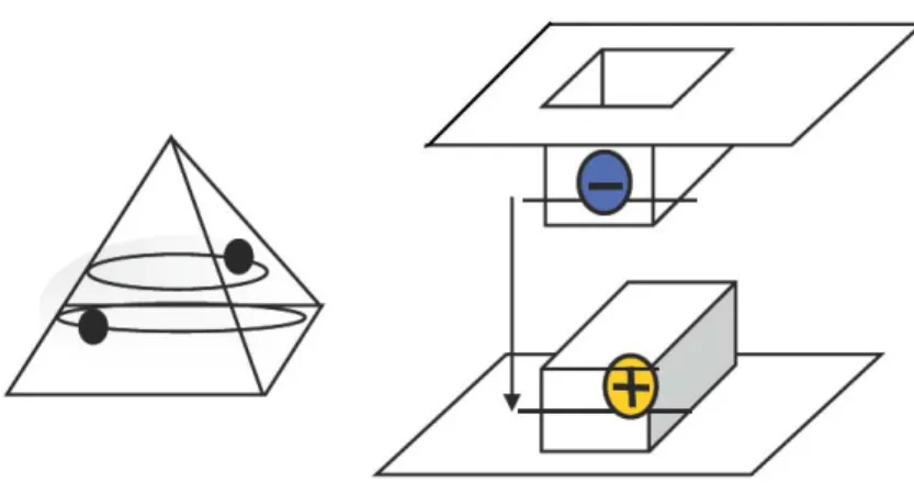
Recently, there have been several approaches to realize nonpolar GaN, m-plane films [24] and m-plane heterostructures [19~20] on γ-LiAlO2(100) as well as a-plane films [25] and a-plane heterostructures [21~23] on r-plane sapphire.The planar relations in hexagonal crystal structure was shown in figure 2.2.1. ZnO and GaN have similar structure, lattice constant, and large band gap. The wurtzite ZnO also have large build in potential if we grown along the [0001] direction.
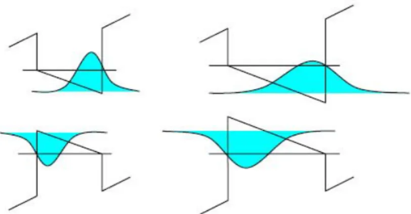
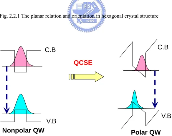
A schematic energy band diagram between nonpolar quantum well and polar c-plane quantum well under QCSE is shown in figure 2.2.2 (a) (b). As can been seen, the well potential in the nonpolar nanostructure is not influenced by the built in polarization field and possess a higher wavefunction overlap and emission energy than polar nanostructure. Thus nonpolar is now a chance to improve the light emitting efficiency greatly and make a grand breakthrough..
2.3 In-plane light polarization effect in nonpolar nanostructure
In addition to the advantage of no internal electric fields in growth direction, nonpolar orientation of the wurtzite crystal structures are also good for polarization-sensitive devices. In contrast to ZnO films grown along the polar c-plane direction, do not exhibit any in-plane polarization anisotropy, m- and a-plane ZnO films, where the c-axis lies in the film plane, exhibit significant polarization anisotropy in its light emission.
When ZnO films are grown on c-plane substrates with similar hexagonal symmetry, there is no linear polarization emission happened under isotropic in-plane strain. However, a ZnO film with an m-plane or a-plane orientation experience anisotropic in-plane strain resulted from the inherent lower symmetry of m and a plane. An in-plane polarization anisotropy has been observed in the PL spectra of GaN/(Al,Ga)N MQWs. [26, 27]
The coordinate system used for the investigation of the polarization properties is x//a [11-20]、y//m [1−100]、and z//c [0001], the three planes are perpendicular to each other. Take the m-plane GaN films for example, m-plane strain lifts the symmetry in the x-y plane of the wurtzite crystal and separates the original |X±iY>-like HH and LH states of unstrained WZ-GaN to |X>-like and |Y>-like states. A compressive strain along x induces a dilatation along y so that the energy of the |X>-like state is raised
while the |Y>-like state is lowered. Valence bands are reconstituted to |X>-like, |Z>-like, and |Y>-like states in order of decreasing electron energy. Therefore, the valence band structure is altered that the lowest transition energy is totally linearly polarized in the x-direction (E⊥C), while the second lowest transition energy is totally linearly polarized in the z-direction (E║C). The third lowest transition energy which is linearly polarized in the y-direction will not show any PL intensity difference when we put the polarizer in x-z plane to get the polarization information. The optical polarization anisotropy in ZnO films with a nonpolar orientation can be used for polarization-sensitive photodetectors [28] and static as well as dynamic polarization filtering [29].
Polar QW
Nonpolar QW
QCSE
C.B
V.B
C.B
V.B
.Fig. 2.2.1 The planar relation and orientation in hexagonal crystal structure
Chapter 3 Theoretical background and experiment apparatus
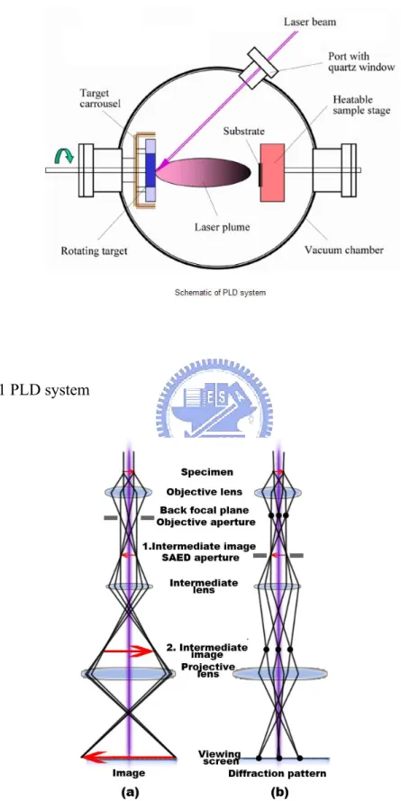
3.1 Growth mechanism of ZnO/ZnMgO MQWs using pulsed laser deposition (PLD) The principle of pulsed laser deposition, in contrast to the simplicity of the system set-up, is a very complex physical phenomenon. It does not only involve the physical process of the laser-material interaction of the impact of high-power pulsed radiation on solid target, but also the formation plasma plume with high energetic species and even the transfer of the ablated material through the plasma plume onto the heated substrate surface. Thus the thin film formation process in PLD generally can be divided into the following four stages.
1. Laser radiation interaction with the target 2. Dynamic of the ablation materials
3. Deposition of the ablation materials with the substrate 4. Nucleation and growth of a thin film on the substrate surface
In the first stage, the laser beam is focused onto the surface of the target. At sufficiently high flux densities and short pulse duration, all elements in the target are rapidly heated up to their evaporation temperature. Materials are dissociated from the target surface and ablated out with stoichiometry as in the target. The instantaneous ablation rate is highly dependent on the fluences of the laser shining on the target. The ablation mechanisms involve many complex physical phenomena such as collisional,
thermal, and electronic excitation, exfoliation and hydrodynamics.
During the second stage the emitted materials tend to move towards the substrate according to the laws of gas-dynamic and show the forward peaking phenomenon. R. K. Singh reported that the spatial thickness varied as a function of cos q. The spot size of the laser and the plasma temperature has significant effects on the deposited film uniformity. The target-to-substrate distance is another parameter that governs the angular spread of the ablated materials. Hanabusa also found that a mask placed close to the substrate could reduce the spreading.
The third stage is important to determine the quality of thin film. The ejected high-energy species impinge onto the substrate surface and may induce various type of damage to the substrate. The mechanism of the interaction is illustrated in the following figure. These energetic species sputter some of the surface atoms and a collision region is formed between the incident flow and the sputtered atoms. Film grows after a thermalized region is formed. The region serves as a source for condensation of particles. When the condensation rate is higher than the rate of particles supplied by the sputtering, thermal equilibrium condition can be reached quickly and film grows on the substrate surface at the expenses of the direct flow of the ablation particles and the thermal equilibrium obtained.
density, energy, ionization degree, and the type of the condensing material, as well as the temperature and the physical-chemical properties of the substrate. The two main thermodynamic parameters for the growth mechanism are the substrate temperature T and the supersaturation Dm. They can be related by the following equation
Dm = kT ln(R/Re)
where k is the Boltzmann constant, R is the actual deposition rate, and Re is the
equilibrium value at the temperature T.
The nucleation process depends on the interfacial energies between the three phases present - substrate, the condensing material and the vapor. The minimum-energy shape of a nucleus is like a cap. For the large nuclei, a characteristic of small supersaturation, they create isolate patches (islands) of the film on the substrate which subsequently grow and coalesce together. As the supersaturation increases, the critical nucleus shrinks until its height reaches on atomic diameter and its shape is that of a two-dimensional layer. For large supersaturation, the layer-by-layer nucleation will happen for incompletely wetted foreign substrates.
The crystalline film growth depends on the surface mobility of the adatom (vapour atoms). Normally, the adatom will diffuse through several atomic distances before sticking to a stable position within the newly formed film. The surface temperature of the substrate determines the adatom's surface diffusion ability. High
temperature favours rapid and defect free crystal growth, whereas low temperature or large supersaturation crystal growth may be overwhelmed by energetic particle impingement, resulting in disordered or even amorphous structures.
In the PLD process, due to the short laser pulsed duration (~10 ns) and hence the small temporal spread (<=10 ms) of the ablated materials, the deposition rate can be enormous (~10 mm/s). Consequently a layer-by-layer nucleation is favoured and ultra-thin and smooth film can be produced. In addition the rapid deposition of the energetic ablation species helps to raise the substrate surface temperature. In this respect PLD tends to demand a lower substrate temperature for crystalline film growth. (Fig3.1.1)
3.2 Transmission Electron Microscope, Energy Dispersive X-ray Spectroscopy (EDS) and Selected Area Electron Diffraction (SAED)
1. Transmission Electron Microscope
Transmission electron microscope is the pre-eminent method for determining dislocation’ and other crystallographic defects character and for performing chemical and crystallographic analysis of micrometer and smaller precipitates and other microstructures. With the similar structure and more powerful function compared with SEM, TEM offers the in-depth perspective of specimen characterizations.
holder and an image recording/viewing system. The objective lens forms a diffraction pattern in the back focal plane with electrons scattered by the sample and gombines them to generate an image in the image plane (1. intermediate image). Thus, diffraction pattern and image are simultaneously present in the TEM. It depends on the intermediate lens which of them appears in the plane of the second intermediate image and magnified by the projective lens on the viewing screen. Switching from real space (image) to reciprocal space (diffraction pattern) is easily achieved by changing the strength of the intermediate lens. In imaging mode, and objective aperture can be inserted in the back focal plane to select one or more beams that contribute to the final image (BF, DF, HRTEM). In selected area electron diffraction (SAED), an aperture in the plane of the first intermediate image defines the region of which the diffraction is obtained.
In the bright field (BF) mode of the TEM, an objective aperture is placed in the back focal plane of the objective lens which allows only the direct beam to pass. In this case, mass-thickness and diffraction contrast contribute to image formation: thick areas, areas in which heavy atoms are enriched, and crystalline areas appear with dark contrast. In spite of the useful information obtainable from BF images, it should be mentioned that the interpretation of contrast is often impeded since these phenomena
In dark field (DF) images, one or more diffracted beams are allowed to pass the objective aperture. The direct beam is blocked by the aperture. In contrast to the direct beam, the diffracted beam has interacted strongly with the specimen, and often very useful information is present in DF images, e.g., about planar defects, stacking faults or particle size.
To obtain lattice images, a larger objective aperture has to be selected that allows many beams including the direct beam to pass. The image is formed by the interference of the diffracted beams with the direct beam (phase contrast). If the point resolution of the microscope is sufficiently high and a suitable sample oriented along a zone axis, then high-resolution TEM (HRTEM) images are obtained. In many cases, the atomic structure of the specimen can directly be investigated by HRTEM.
The incident parallel electron wave interacts elastically while passing through the specimen, and the resulting modulations of its phase and amplitude are present in the electron wave leaving the specimen. The wave here, the object exit wave o(r), thus contains the information about the object structure. The objective lens performs 1. The Fourier Transform (Fourier analysis) that creates the diffraction pattern of the object in the back focal plane and 2. the inverse Fourier Transform (Fourier synthesis)
that makes the interference of the diffracted beams back to a real space image in the image plane (lattice image).
2. Energy Dispersive X-ray Spectroscopy & Selected area Electron diffraction
EDS and SAED are two auxiliary function affiliated to SEM/TEM and TEM respectively. Both of them are used to characterize samples based on the constituents and structures. Energy dispersive X-ray spectroscopy (EDS or EDX) is an analytical tool predominantly used for chemical characterization. Being a type of spectroscopy, it relies on the investigation of a sample through interactions between light and matter, analyzing X-rays in its particular case. Its characterization capabilities are due in large part to the fundamental principle that each element of the periodic table has a unique electronic structure and, thus, a unique response to electromagnetic waves. The excess energy of the electron that migrates to an inner shell (in order to fill the newly-created hole) can do more than emit an X-ray. Often, instead of X-ray emission, the excess energy is transferred to a third electron from a further outer shell, prompting its ejection. This ejected species is called an Auger electron, and the method for its analysis is known as Auger Electron Spectroscopy (AES). X-ray Photoelectron Spectroscopy (XPS) is another close relative of EDS, utilizing ejected electrons in a manner similar to that of AES. Information on the quantity and kinetic energy of
ejected electrons is used to determine the binding energy of these now-liberated electrons, which is element-specific and hence allows chemical characterization of a sample. EDS is often contrasted with its microscale spectroscopic counterpart, WDS (Wavelength-Dispersive X-ray Spectroscopy). WDS differs from EDS in that it uses the diffraction patterns created by light-matter interaction as its raw data.
Selected area Electron diffraction, abbreviated as SAED, is a crystallographic experimental technique that can be performed inside a transmission electron microscope (TEM).
In a TEM, a thin crystalline specimen is subjected to a parallel beam of high-energy electrons. As TEM specimens are typically ~100nm thick, and the electrons typically have an energy of 100-400 kiloelectron volts, the electrons pass through the sample easily. In this case, electrons are treated as wave-like, rather than particle-like (see wave-particle duality). Because the wavelength of high-energy electrons is a fraction of a nanometer, and the spacings between atoms in a solid is only slightly larger, the atoms act as a diffraction grating to the electrons, which are diffracted. That is, some fraction of them will be scattered to particular angles, determined by the crystal structure of the sample, while others continue to pass through the sample without deflection.
As a result, the image on the screen of the TEM will be a series of spots -- the selected area diffraction pattern, SADP, each spot corresponding to a satisfied diffraction condition of the sample's crystal structure. If the sample is moved under the beam, bringing different sections of it under illumination, the arrangement of the spots in the diffraction pattern will change. If the sample is tilted, the same crystal will stay under illumination, but different diffraction conditions will be activated, and different diffraction spots will appear or disappear.
SAD is referred to as "selected" because the user can easily choose which part of the specimen to obtain the diffraction pattern from. Located below the sample holder on the TEM column is a selected area aperture, which can be inserted into the beam path. This is a thin strip of metal that will block the beam. It contains several different sized holes, and can be moved by the user. The effect is to block all of the electron beam except for the small fraction passing through one of the holes; by moving the aperture hole to the section of the sample the user wishes to examine, this particular area is selected by the aperture, and only this section will contribute to the SADP on the screen. This is important, for example, in polycrystalline specimens. If more than one crystal contributes to the SADP, it can be difficult or impossible to analyze. As such, it is useful to select a single crystal for analysis at a time. It may also be useful
to select two crystals at a time, in order to examine the crystallographic orientation between them.
As a diffraction technique, SAED can be used to identify crystal structures and examine crystal defects. It is similar to x-ray diffraction, but unique in that areas as small as several hundred nanometers in size can be examined, whereas x-ray diffraction typically samples areas several centimeters in size.
3.3 Photoluminescence
Photoluminescence, a powerful and breakless analysis technology, can reveal the band structure and the carrier transportation behaviors in a material. Moreover, the doping type, band gap, composition, etc. of the bulk material or the size, path of carrier transportation, lifetime, etc. of the nano-material will be shown in the photoluminescence spectrum.
Photoluminescence is a process in which a chemical compound absorbs photons (electromagnetic radiation), transitioning to a higher electronic energy state, and then radiatives photons back out, returning to a lower energy state. The period between absorption and emission is extremely short, on the order of 10 nanoseconds. Light is directed on a sample, where it is absorbed and imparts excess energy into the material
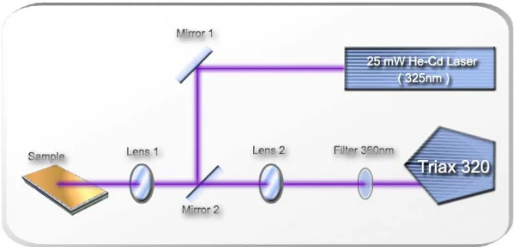
is called photoluminescence (PL). The intensity and spectral content of the photoluminescence is a direct measurement of various important material properties. Fig 3.3.1 shows the schematic setup of PL system with He-Cd laser operating at 30mW at the wavelength of 325nm.
Typically, the process of the luminescence consists of three steps, which is (1) excitation, (2) thermal equilibrium and (3) recombination. Through thermal equilibrium, electron-hole pairs (e-h pairs) generated by incident light recombine and create photon. In the energy band gap, impurities and defects form a variety of energy levels, whose corresponding energy produces radiation through radiative recombination and absorption through non-radiative recombination.
3.4 Absorption
If the energy is delivered by incident photons the process is called optical absorption. A number of different phenomena may be associated with the incidence of light on a semiconductor. Fig 3.4.1 shows a schematic of the optical absorption spectrum vs. energy of the photons. For our discussion here, phenomena related to (2) excitons, (3) fundamental absorption processes and (4) impurities are of interest. For the absorption process the density of states N (E) is of importance, where E is the energy. Due to the uncertainty relation, the volume necessary per state in the
are assumed to be spheres. Hence, considering the spin of the electron, the volume in
the momentum space between E+dE is 2×4πp2dp We write N(E) in the momentum
space as 2 3 8 ( ) N E dE p dp h π = From p= 2 *m E , it follows 1 2 * 2 dp m dE E = and we find ( ) (2 *)2 33/ 2 2 m N E EdE π =
= with the dimension cm
-3
eV-1.
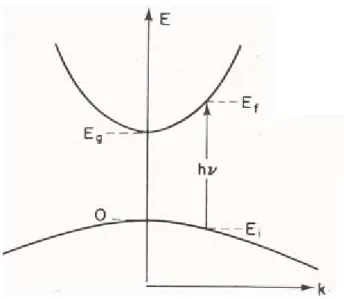
Let us consider now absorption transitions between two direct valleys where all the momentum-conserving transitions are allowed (see fig 3.4.2), i.e., the transition probability Pif is independent of the photon energy. Every initial state at Ei is associated with a final state Ef such that Ef=hν-|Ei|.
Therefore, for parabolic bands, we get
2 2 * * 1 1 2 g e h k h E m m ν − = ⎛⎜ + ⎞⎟ ⎝ ⎠ = Eq(3.4.1)
where, the me and mh is the effective mass for electrons and holes, respectively. The reduced effective mass is
**e *h* r e h m m m m m = + Eq(3.4.2) Finally, the density of states for a direct transition is given by 3/ 2 1/ 2 2 3 (2 ) ( ) ( ) 2 r g m N E hv E π = − = Eq(3.4.3) ( ) ( ) c e E n=
∫
∞ N E f E dE ( ( ) 1 1 f E E kT f E e − = + ) Eq(3.4.4)we find
(
)
3/ 2 * 2 2 exp / 2 e F c m kT n E E kT π ⎛ ⎞ ⎡ ⎤ = ⎜ ⎟ ⎣ − ⎦ ⎝ = ⎠ Eq(3.4.5) and(
)
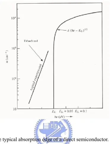
3/ 2 * 2 2 exp / 2 h v c m kT p E E kT π ⎛ ⎞ ⎡ ⎤ = ⎜ ⎟ ⎣ − ⎦ ⎝ = ⎠ Eq(3.4.6)where Ec and Ev mark the energy of the conduction and valence band, respectively. Although we know the density of states and the carrier contribution, we are not able yet to plot the absorption spectrum of a semiconductor, i.e…, the absorption coefficient as a function of the energy since equation 3.4.3 creates a “severe problem”. At hν=Eg, N (E) =0. Theoretically, it is the correct answer but in reality this is always wrong. The density of states is not nil at the band gap of the material. The main reason is the band tails, i.e., a perturbation of the conduction and valence bands by the formation of tails of states extending the bands into the energy gap. An ionized donor exerts an attractive force on the conduction electrons and a repulsive force on the valence holes (acceptors act conversely). Since impurities are distributed randomly in the host crystal, the local interaction will be more or less strong depending on the local crowding of impurities (see fig 3.4.3).
It should be noted that the local energy gap - the separation between the top of the valence band and the bottom of the conduction band is everywhere maintained constant. But the density-of-states distribution, which integrates the number of states
at each energy inside the whole volume shows that there are conduction band states at relatively low potentials and valence band states in high-potential regions. The transition between the band tails causes an exponentially increasing absorption coefficient α (d (lnα) /d (E) =1/kT) and is known as Urbach’s rule. The exponential absorption edge of GaAs was found to correlate quite well with transitions involving band tails, which can be controlled by doping. Figure 3.4.4 shows the typical absorption edge of a direct semiconductor.
For the plot of α (E), we write down according to equation 3.4.3
1/ 2
0
( )E I A E( Eg)
α = − Eq (3.4.6)
and Urbach’s rule
( )E K0exp
(
E Eg)
kTσ
α = ⎡⎢ − ⎤⎥
⎣ ⎦ Eq(3.4.7)
where A0 and K0 are fitting parameter and σ is a phenomenological parameter scaling the steepness of the absorption edge. The absorption coefficient can be plotted over energy applying the continuity equations
( )α E I =α( )E II Eq (3.4.8)
and d
( )
E I d ( )E IIdE dE
α α
= Eq (3.4.9) We find for cross-over energy between α (E) I and α (E) II, 2 ch g kT E E σ = + Eq (3.4.10) Therefore, the absorption edge is described by,
( ) ( )1/ 2 g h A h E α ν = ν − if hν ≥Ecr Eq (3.4.11)
and
( )h A 2kT exp(
h E)
kT σ σ σ α ν = ⎧⎨ ν − ⎫⎬ ⎩ ⎭ if hν ≤Ecr Eq (3.4.12)Fig 3.1.1 PLD system
Fig. 3.2.1 (a)Ray diagram for viewing the image and (b) the diffraction pattern of the sample.
Fig 3.3.1 The schematic diagram of photoluminescence setup
Fig 3.4.1 Different types of optical absorption phenomena; (1) transitions of high-lying bands, (2) excitons, (3) fundamental absorption (4) impurity absorption, (5) free-carrier absorption and (6) Reststrahlen absorption
Fig 3.4.2 The momentum-conserving transitions are allowed
Fig 3.4.3 The left diagram shows the perturbation of the band edges by Coulomb interaction with inhomogeneously distributed impurities. This leads to the formation of tails of states shown on the right side. The dashed lines show the distribution of states in the unperturbed case.
Figure 3.4.4 The typical absorption edge of a direct semiconductor.
Fig 3.4.5 Absorption system
SIGNAL RECOVERY X Y 64.02 mV 15.66 mV INPUT LIMIT 3V AC GAIN 0dB SEN 200mV TC 500ms FRQ 200Hz DR 60 monochromator 600 1200 Lamp NCUE Optical chopper Black box Lock-in Amplifier Chopper driver
Stepping motor driver
Lens GBIP 8255 Chopper Photodetector Sample Lens Polarize
Chapter 4 Basic optical characteristics of a-plane ZnO/ZnMgO
MQWs
In this chaper, we discuss the basic optical characteristics of a-plane Zno/ZnMgO MQWs. In section 1, we describe the method how we prepare the samples and the growth conditions. In section 2, we discuss the PL spectra of the samples and finite square well model is used to estimate the emission energy of our samples. In section 3, power dependent PL reveals nonpolar ZnO/ZnMgO MQWs is free from QCSE. In section 4, temperature dependent PL shows localization effect is unobvious and the activation energy fitting result shows exciton binding energy enhance by quantum confinement. In section 5, The absorption spectrum was carried out to reveal different recombination paths since the asymmetry strain along c-axis and m-axis which caused valence band splitting. Furthermore, the 92% high polarization of degree of ZnO/ZnMgO MQWs emission was also obtained at 20 K. 4.1 Samples preparation and growth
A KrF excimer laser with λ=248nm was used for PLD deposition of ZnO and
ZnMgO films. The base pressure in the growth chamber was 1×10-18 Torr. After
degreasing in boiled acetone and isopryl alcohol, a 2 inch r-plane sapphire substrate was loaded into the PLD chamber and heated in high vacuum at 850°C for 30 min. Then, the oxygen flow was introduced to the chamber in which the oxygen partial
pressure was then kept at 1.4×10⁻² Torr for the rest duration of deposition. The targets in the chamber were 2 in pure ZnO and Zn0.8Mg0.2O sintered ceramics. For ZnO film (buffer layer), it was deposited in high vacuum for 5 min at 490°C, and then deposited
in oxygen atmosphere at 800°C for 140 min. For five-period ZnO/Zn0.8Mg0.2O film
structures, the deposition condition for the first ZnO buffer layer was kept the same as described above, followed by the growth of QWs at 650°C with the thickness of each
layer varied by changing the deposition time. Zn0.8Mg0.2O (barrier layer) was
deposited for 3 min, and ZnO (well layer) was deposited in vacuum for 1.5 min.
Finally, Zn0.8Mg0.2O (capping layer) was deposited for 5min. For ten pairs ZnO/
Zn0.8Mg0.2O MQWs growth, ZnO film (buffer layer) was deposited in high vacuum
for 2 min at 750°C, and then deposited in oxygen atmosphere at 750°C for 40 min, and Zn0.8Mg0.2O (buffer layer) was deposited at 750°C for 31 min. ZnO (well layer) was deposited at 750°C for 40 sec, and Zn0.8Mg0.2O (barrier layer) was deposited at 750°C for 70 sec. Micro-structural characterization was carried out using cross-sectional transmission electron microscopy (TEM) in the Fig. 4.1.1 (a) (b) 4.1.2 (a) (b). The X-ray energy-dispersive spectroscopy confirmed that the Mg composition
of the quantum well is around 20%. For the five pairs ZnO/Zn0.8Mg0.2O MQWs, ZnO
buffer layer is around 300nm thick, the Zn00.8Mg0.2O barrier width is around 8.3 nm thick, and the ZnO well width is around 5.6 nm thick. As for the ten pairs ZnO
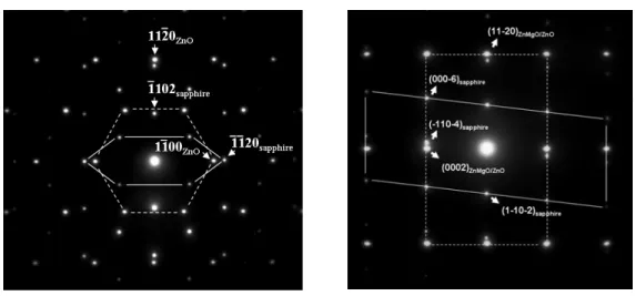
/Zn0.8Mg0.2O MQWs growth, ZnO buffer layer is around 300nm thick, Zn0.8Mg0.2O buffer layer is around 100nm, the Zn00.8Mg0.2O barrier width is around 2.3 nm thick, and the ZnO well width is around 1.8 nm thick. The selected area diffraction (SAD) pattern shown in Fig. 4.1.3 (a) (b) is obtained from the interface between the ZnO layer and sapphire substrate where electron beam is from c-axis (m-axis) in Fig 4.1.3(a) (Fig. 4.1.3 (b)). The crystal plane of (1-100) ZnO parallels to (11-20) sapphire and (000-1) ZnO parallels to (1-10-1) sapphire.
4-2 Photoluminescence spectra of a-plane ZnO/ ZnMgO MQWs
Low temperature PL measurements were performed using the cw 325 nm He–Cd laser operating at an excitation level of 25 mW. Fig. 4.2.1 shows the PL spectra of
a-plane ZnO /Zn0.8Mg0.2O MQWs at 20K. The peak energy of film a-plane ZnO film
is at 3.375eV which is slightly larger than c-plane ZnO film (~3.36eV) .The peak
energy of five pairs ZnO/Zn0.8Mg0.2O MQWs is about 3.407eV which is blue shift
about 32meV. The paek energy of ten pairs ZnO/Zn0.8Mg0.2O MQWs is about
3.538eV which is blue shift about 163meV. The PL spectra also display the emission
from the buffer layer which is around 3.37eV (D0X) and 3.318eV (e-A
0) in all
samples. [30].
Room temperature PL was also performed in the Fig 4.2.2 (a) (b). Finite-squqre well model was used to calculate the peak energy of the five & ten pairs
ZnO/Zn0.8Mg0.2O MQWs that takes into account the exciton binding energy. The exciton energy in the QW is calculated by Eq(4.2.1).
QW ZnO QW
ex g e h b
E =E + Δ + Δ −E E E Eq(4.2.1) ZnO
g
E is the band gap energy of ZnO, △Ee and △Eh are the confinement energies of
electrons and holes, respectively, QW b
E is the exciton binding energy in QWs. EgZnO
is 3.37eV[31] and the exciton binding energy is about 60meV. Because the PL spectra
of five pairs ZnO/Zn0.8Mg0.2O MQWs includes the emission of QWs and buffer ZnO,
the peak energy was fitted by lorentzian waveform. The effective mass of electron is 0.28m0 and the effective of hole is 0.58m0. (m0 is electron mass) The band-offset ratio is 60:40. The energy of ZnxMg(1-x)O is calculated by Eq(4.2.2). [32][33]
ZnxMg(1-x)O=3.37+2.51x(eV)………. Eq(4.2.2)
For five pairs ZnO/ZnMgO MQWs, the calculation result was 3.35eV. For ten pairs ZnO/ZnMgO MQWs, the calculation result was 3.506eV. The slight different may casue from the enhancement of exciton binding energy, the single quantum well approach…..etc.
4.3 Nonpolar characteristics of a-plane ZnO/ ZnMgO MQWs
In c-plane polar structure, the built-in field with the MQWs would lead to band tilting. If the photo-genarated carriers were injected into the MQWs, the built-in electric field could be screened and result in a blue-shift of PL energy peak
[34]. As we mentioned above, the useful approach for reducing the built-in electric field is to grown MQWs along the nonpolar direction. In this section, we performed the power dependent photoluminescence to realize the built-in field influence on our samples.
The power dependent photoluminescence was demonstrated by using He-Cd laser operated at 325 nm. The excitation power increased from 0.05 to 35 mW. Fig.4.3.1 (a) (b) showed the PL spectra as a function of excitation power for our samples at low temperature. Morhain C et al had calculated the built-in electric field in polar ZnO/ZnMgO MQWs and his experiment result showed when power density vary
from 0.1 mW/cm2 to 100W/cm2 the PL spectra was under large blue–shift(~80meV).
Fig 4.3.2(a) (b) showed power-dependent PL results, which exhibited the un-shifted peaks in a-plane ZnO/Zn0.8Mg0.2O MQWs as increasing pumping power density. It is well known for a-plane hexagonal MQW with the non-polar characteristic and the flat-band structure demonstrates that the structure possesses free electric field. We also analyzed different power dependences I~Pα for a-plane ZnO/Zn
0.8Mg0.2O MQWs
where I is the integrated PL intensity, P is the excitation power density, and α is the power index. α value is around 1. We exclude out the influence non-recombination which also imply no built-in electric field in this structure in terms of our fitting result.
4.4 The localization effect of a-plane ZnO/ZnMgO MQWs
In order to further understand whether the localization effect plays an important role in nonpolar ZnO MQWs or not, the PL spectra were measured under different temperature in the range of 20K to 300K using the CW 325 nm He–Cd laser.
Fig. 4.4.1 (a) (b) shows the evolution of PL spectra as a function of temperature for the a-plane ZnO/ZnMgO MQWs. The decrease of PL intensity with increasing temperature is observed. Thermal quenching PL intensity with increasing temperature is a general phenomenon in semiconductor nanostructure which is caused by carriers thermalization from the radiative recombination centers or/and localized states to the nonradiative recombination centers or/and delocalized states. This thermal quenching behavior will be discussed later.
The emission from the buffer layer is strong at low temperature (~20K), but as the temperature got raised the emission from quantum well will dominate the PL spectra. This is evidence that excitons are confined in quantum well, because the thermal quenching in quantum well is smaller than in buffer layer. In order to check the situation of alloy and interface fluctuations in our samples, we further analyze the peak shift of ZnO/ZnMgO MQWs emission over the investigation temperature range. The result is shown in Fig. 4.4.2 (a) (b). In our samples, the emission energy decreases monotonically with increasing temperature. We didn’t observe the exciton
localization effect [35] [36] which may induce red-blue-red shift(S-curve) of peak energy with increasing temperature. It seems no deep localization states in the ZnO/ZnMgO MQWs system. In InGaN/GaN MQWs system, S-curve is a very common phenomenon. Inhomogeneity due to interface fluctuation, InN/GaN segregation, and the band tail states originating from the high density of defects are responsible for the so-called S-shaped temperature dependent behavior in the InGaN/GaN MQWs. Whereas there is no this relevant problems with well material of ZnO so that ZnO/ZnMgO MQWs is more stable and the localization center is more uniform in comparison to InGaN/GaN MQWs.
Figure 4.4.3 show the Arrhenius plot of the normalized integrated PL intensity for the a-plane Zno/ZnMgO MQWs emission from MQWs over the temperature range under investigation. The intensity reduction is remarkable, the degree of PL intensity reduction from 20K to 300K is more severe when the well width gets thicker which indicates a higher PL efficiency in the thinner well width samples [35]. We use the equation below to get a good fit to our experimental data of the activation energy in thermally activated processes [37].
I (T) = I0/ [1+a*exp (-Ea/KBT) +b*exp (-Eb/KBT)] Eq. (4.4.1) Where I (T) is the temperature dependent integrated PL intensity, I0 is the integrated PL intensity at 20K, KB is the Boltzmann’s constant, a and b are the rate constants,
and Ea and Eb are activation energy for two different non-radiative channels. This suggests that there are two non-radiative paths exist at the same time which one of them dominates in the low temperature region and the other dominate in the high temperature region.[38]
Since the activation energy we get from our samples is much less than the bandgap energy difference between the well and the barrier. It is impossible to account the thermal quenching of ZnO MQWs emission for carriers thermalized from the ZnO wells to the ZnMgO barriers. Therefore, the more reasonable explanation for the quenching of luminescence is that increasing temperature increases the probability of excitons to be trapped by nonradiative recombination centers within the well at the same time when carriers are activated out of the loacalization minima of potential fluctuation which may be caused by compositional、interface fluctuation. Or the excitons partly dissolve into free carrier which may be trapped by nonradiative recombination centers. The smaller activation energy was attributed to the shallow localization states forming in the interface fluctuation of well and barrier layer. The larger activation energy was attributed to the enhancement of the exciton binding energy [39]. Giuliano Coli et al had calculated the enhancement of the exciton binding energy due to quantum confine effect [40]. As temperature rose, excitons partly dissolved into free carriers which may decrease the
efficiency of excitons recombination. Furthermore, the free carriers may be trapped by non-radiative centers which also decrease the emission intensity. In our fitting result, the enhancement of binding energy is larger in thin ZnO/ZnMgO MQWs. 4.5 In-plane polarization effect of a-plane ZnO/ ZnMgO MQWs emission
4.5.1 In-plane polarization effect of a-plane ZnO/ ZnMgO MQWs emission
It was mentioned in section 2.3 that due to the inherent lower symmetry of
non-polar heterostructure, a-plane ZnO/ZnMgO MQWs is likely to experience anisotropic in-plane strain. A PL measurement was carried out at low temperature using the CW 325nm He-Cd laser and a visible polarizer was set in front of the spectrometer to examine the polarization property of our samples. In the case, of the a-plane ZnO/ZnMgO MQWs, an angle of 90° is defined to be perpendicular to the c
[0001] axis (E⊥C) while the 0° is along m [1−100] axis (E∥C). Fig 4.5.1 (a) (b)
display the polarization–dependent PL spectra of our samples for polarization angles between 0° and 90° in steps of 15°. The value of polarization degree ρ is defined as ρ= (I⊥-I║) / (I⊥+I║) Eq. (4.5.1)
, where I⊥and I║ are PL intensities for E⊥C and E║C. Fig 4.5.2 (a) (b) showed the
pretty symmetric of the normalized PL intensity versus the in-plane polarization angle. The polarization degree ρ of our samples are 92%、84.8% for five pairs MQWs and ten pairs MQWs, respectively. This high polarization ration phenomenon was