A New
Single-phase
On-Line
UPS
Structure
Pre-staged with PFC-and-Boost Converter
Wen-Jung Ho, Mu-Shen Lin, Wu-Shiung Feng
Department of Electrical Engineering National Taiwan University
Taipei 10617, Taiwan
Abstract
This paper presents a new on-line uninterruptible power supply (UP9
structure in which a dual-functional PFC substitutes for an inevitable battery-voltage booster thereby simplifiing the complexity of power stage. Via the proof of experimental
results, the proposed UPS structure consequent& shows its feasibi/i@, low cost and high power density.
1.
Introduction
With information industry
prospering, unintermptible power supply (UPS) is used widely and getting more and more important [l-SI. But the utility system is usually contaminated by those critical equipment, thus power-factor- correction (PFC) pre-regulator served as the rectifier of UPS is a growing trend
[3,4]. For a designer, however, it is always a dilemma between adding an extra-PFC and reducing cost.
Fig. 1 shows the functional block diagram of conventional on-line
U P S
which consists of a PFC, inverter, charger, boost converter, and a battery set [ 1,2]. When the mains is present, AC power source goes through PFC then inverter in order to supply the regulated
AC power to the load, and the charger simultaneously energizes the batteries, i.e. the functional block marked with # will be active. In the meantime, the boost converter is inactive. Unless when the mains fails, i.e. the functional block
with mark @ will be active, it will startup to lift battery-voltage toward original DC-link voltage level to energize DC capacitor. Thus the following inverter stage can still work normally because of keeping same
DC-
link voltage level of inverter input. Due to the pre-regulator of PFC, this is an
inevitable procedure because
commonly-used boost-type
PFC
always has high DC output.In another words, if DC-link voltage of the P E ’ s ouput is around 240V
DC
and without lifting of booster, it will need about 20 12V-batteries connected in series (totally 240V DC) to r e ~ n working normally during blackout phase.
A 1KW UPS, e.g., will need 20 rarely- used 12V/l. SAH-batteries to supply 10
minutes of back-up time (general specification for
UPS)
[l]. If there is a battery-voltage booster, however, it can just use 5 commonly-used 12V/7AH- batteries, or other cheaper and available ones, to do so. The more common battery types are, the cheaper they usually are. Furthermore, the more batteries U P S has, the more complicatedand less reliabe connection it has.
Now that the battery-voltage booster is inevitable as well as input current harmonics reduction may be also mandatory, this paper uses PFC as pre- regulator and its sub-function substitutes for the conventional boost converter such that it can simplify UPS structure. It is needless to use unusual and expensive battery types to fit DC-link voltage for specified back-up time.
II.
The Proposed
UPS
A. System DescriptionFig. 2 shows the functional block diagram of the proposed on-line UPS. It consists of
a
dual-functional PFC, inverter, charger, battery-switch, and a battery set The operation principles can be also traced by the marks # and @,of the functional blocks. And, the practiced power circuit of the proposed UPS is shown as in Fig. 3.By comparison, it is obviously more economical than the conventional
U P S structure because it exploits the
PFC to the most for saving a conventional boost converter. When the mains is normal, switch SI of the dual- fiulctional PFC is controlled to shape the input current to be sinusoidal, switches S2 and S3 of the push-pull inverter are operated in a sinusoidal PWM fashion accompanied with output Lo/Co filter to generate output voltage, and the flyback charger works normally to charge the battery set (battery-switch open).
As soon as the mains is gone, the battery-switch will be closed
immediately, switch Si are controlled as DC voltage booster’s main-switch to step-up battery voltage, switches S2 and
S3 are still operated in the same sinusoidal PWM fasluon but the charger
will shutdown for no AC input. Both
ACDC battery charger and DCIAC
inverter have been the source of interest in so many literatures of power electronics field, thus they would be very resourceful [3-81. Therefore, the know-how parts of the proposed
U P S
isjust the dual-functional PFC whose descriptions and analyses are in the following section.
B. Dual Functional PFC
Fig. 3 shows the equivalent circuit of the proposed dual functional PFC which needs a state-switch to change its operation mode. While battery-switch is open, the state-switch i s on (I) position. While battery-switch is closed, the state- switch is on (11) position. Single-switch boost-type PFC and conventional single- switch DC-DC boost converter have same main components of power-stage circuits. And, no matter whether the main-switches turn on or off, they also exhibit the same equivalent circuits
--
they can be combined together.The operation principles can be divided into two modes along with its main-switch’s current-related variety shown as follows:
mode (I): The state-switch is on (I) when the mains is normal. The converter serves as a PFC function which shapes input current waveforms to be sinusoidal and generates DC output by controlling switch Si in PWM fashion. In this period, its main-switch’s peak current I s p ~ , peak) can be expressed as
I s p x , peak) = I . 4 I 4 xPouNin(minimum) ( 1 )
where Pout is the output power and
Vin(minimum) is the minimun value of
input voltage.
when the mains is absent. The dual- fwctional converter serves as a DC- voltage booster of the PFC's sub- function. By using the same PFC's control logic and feedback circuits, the main switch SI can also be controlled in PWM fashion to boost battery voltage, b , u p to same DC output level. In this period, its main-switch's peak current Is
(boost, p e d ) can be expressed as
IS (boost, peak) = IO x VO / vB(minimum) (2)
where Io is output current, vB(mzHii?ZUm) is
the minimun value of low-battery voltage, and Vu is output voltage.
Therefore, from Eq.(2)
-
Eq.(l), the current difference hls &a~) of mode (I)and mode (11) can be expressed as
For example, Vin(minimum) = 90V AC,
VB(minimum) = 40V DC, Vo = 250V DC,
and load is 1kW. Then
Ah
(ped, E 9.3A. Therefore, if VB is not too low, the current difference of main-switch for the two modes will be acceptable. Thus they can share a common circuit if we can choose a proper current-rating capacity for the main-switch.Because the control logic and feedback circuits of the proposed converter are based on mode (I)
--
input- current-shaping feature, we should consider if mode (U) is stable for this kind of application. Though there aretwo points to confirm it is stable: 1)
Mode (11)'s power-circuit cell is delayed only 90" for small-signal model because it has an inner controlling loop, which is continuous conduction mode (CCM) PFC's inherent stuff, can cancel one pole of original 180" power-circuit cell
[9,10]. There is no stability problem of feedback for a 90"-delayed controlling plant. 2) Mode
(a)
is just one operationpoint of mode (I) because VB should be
within the swing of input voltage for a plausible design. Furthermore, the PFC circuits usually have narrow bandwidth because the outer controlling loop has to be filter low-frequency AC-line ripple voltage, i.e. it leads to low step-response [9, lo]. However, the following DC-AC inverter should be designed to compensate this deficiency by using wider bandwidth feedback circuit to make it have better response.
111.
Experimental
Results
To verify the feasibility of the proposed UPS, an 1KW
U P S
(Vin =110V AC / 60HZ) power-stage shown as
Fig. 3 along with proper logic and
feedback circuits was well implemented. Its DC-link voltage is 250V DC. The battery set has 5 12VIGAH-batteries with
10 minutes of back-up time for firll-load. And, the flyback charger can supply 68V DC constantly to charge the battery set (current limit is 1 A) during AC- line normal operation.
Fig. 5 shows the input waveforms
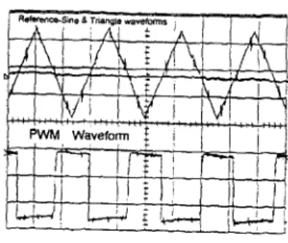
of the proposed U P S when the mains is normal. The dual-functional PFC performs mode (I) operation. We can find the input current is virtually sinusoidal and synchronized with the input voltage. Comparably, Fig. 6 also shows the input waveforms while the PFC does not startup. Fig. 7 illustrates internal PWM waveforms generation of
the U P S ' S control board along with its zoomed figure of Fig. 8. Fig. 9 is the output waveforms with Eull-load during normal operation. Fig.10 shows the transferring waveforms of output voltage from mode
(E)
to mode (11), i.e. fiom mains nornmal to blackout. "here is just a little bit glitch on ti. Fig. 11exhibits the waveforms of load changing during outage, including the autput
voltage and current. Initially, t = to
-
ti,the
U P S
was not imposed on any load.In the meantime, Io = 0 and Vo keeps stable voltage. At t = ti, a full-load (cold lamp) rushed into the UPS resulting in
a
cycle of voltage sagged around 70% of stable voltage. Then after 3 cycles of fluctuation, at t = t2, it back into stablestatus again. Additionally, the main- switch SI can keep its temperature around 60" C under 20° C of surrounding, i.e. inQcates small cunent difference of operational modes.
1V.
Conclusions
In this paper a new single-phase on- line UPS structure with pre-staged dual- hctional PFC has been proposed. The key parts, dual-functional PFC, is pre- staged for the proposed UPS and works as a boost converter during outage such that it can simplify the complexity of UPS structure. With economy-oriented power stage and good performance, the proposed structure can be a good candidate in the on-line UPS application.
INVERTER
Fig.1: Functional diagram of conventional single-phase on-line UPS.
When mains normal, the blocks with #
indicate active otherwise is inactive. When main failed, the blocks with @
indicate active otherwise is inactive.
DC-LINK OUTPUT INVERTER D C l A C "A B L r r W Y s y l l i t n - CHARGER = - @ T E R E S
Fig.2: Functional diagram of the proposed UPS. When mains normal, battery-switch open, the blocks with ##
indicate active otherwise is inactive. When main failed, battery-switch closed, the blocks with @ indicate active otherwise is inactive.
Fig.3: The proposed UPS structure using dual functional PFC.
Fig.4: The equivalent circuit of the proposed dual-functional PFC.
Fig.5: The input waveforms of the proposed UPS when the mains is
normal,
Vin (SOV/div) and Ii (SNdiv).
Fig. 8:
of Fig. 7 (20 yddiv, 2.0 Vldiv).
The zoomed PWM waveforms
Fig. 6: The input waveforms without starting up the PFC when the mains is
normal, Vin (SOVidiv) and Ii (5Ndiv).
Fig. 7: The internal PWM waveforms generation of the the proposed U P S ,
(0.2 ms/div, 2.0 V/div).
Fig. 9: The output waveforms of the the proposed UPS With full-load, Vo (SOV/div) and Io (SNdiv).
Fig.10: The transferring waveforms of
output voltage &om from mains nommal
Fig.11: The output waveforms of changing load for the proposed U P S
V.
References
[l] D. C. GrifRh: ”Unintermptible Power Supplies: power conditioners for critical equipment,” Marcel Dekker, Inc., New York, pp.157-339, 1989. Recommended Practice for Powering and Grounding Sensitive Electronic equipment ,” IEEE Emerald Book, pp.
[3] Yuasa Corporation, Osaka, Japan,
“ Development of UPS using new type
of circuits,” IEEE 1NT.ELEC ’94, Con$ Proceedings, pp. 635-642.
[4] I. Kubo, Y. Ozawa, R. Nakatsuka, A.
Shimizu, “A fully digital controlled UPS using IGBT’s,” IEEE IAS’91, Con$
Proceedings, pp. 1042- 1046.
15) R. G. Kessler and E.D. McGee, “New UPS Architectures Meet demands for Continuous, Clean Power to Critical System,” Powertechnics Magazine, Nov. [6] S. Martinez, M. Castro, R. Antoranz,
and F. Aldana, “Off-line Unintermptible
Power Supply
with
Zero Transfer Time Using Integrated Magnetics,” IEEE Trans. Ind. Electron., Vol. 36, No. 3, pp.[2] JEEE Std 1100-1992: “IEEE
159-197, 1992.
1986, pp. 13-16.
441-445, Aug. 1989.
[7] G. J. Smollinger and W. J. Raddi, “Reverse Energy Transfer Through an AC Line Synchronized Pulse Width Modulated Sine Wave Inverter,” IEEE
Int. Telecommunicat. Energy Con$, Intelec 81, pp. 126- 13 1.
181 W. J. Raddi and R. W. Johnson, “An
Utility Interactive PWM Sine Wave Inverter Configured as a High Efficiency
UPS,” IEEE Int. Telecommunicat. Energy Conf.’, Intelec 8 I , pp. 126- 13 1. [9] Vincent G. Bello, “Using The SPICE-2 CAD Package for Easy Simulation of Switchsng Regulators Both Continuous And Discontinuous Conduction Modes,” Proceedings of
Powercon 8, pp. 1-13, 1981.
[lo] R. B. Ridley, B. H. Cho, F. C. Lee,
“Analysis And Interpretation of LOOP
Gains of Multiloop-Controlled
Switchmg Regulators,” IEEE Trans. on Power electronics, pp. 489-498, Vol. 3,