DESIGN AND IMPLEMENTATION OF A RECONFIGURABLE FIR FILTER
Kuan-Hung Chen
andTzi-Dar Chiueh
Graduate Institute of Electronics Engineering and Department of Electrical Engineering,
National Taiwan University, Taipei, Taiwan
106
17
ABSTRACT
Finite impulse response (FIR) filters are very impor- tant blocks in digital communication systems. Many ef- forts have been made to improve the filter performance, e.g., less hardware and higher speed. In addition, software ra- dio has recently gained much attention due to the need for integrated and reconfigurable communication systems. To this end, reconfigurability has become an important issue for the future filter design. In this paper, we present a digit- reconfigurable FIR filter architecture with the finest granu- larity. The proposed architecture is implemented in a single- poly quadruple-metal 0.35-pm CMOS technology. Mea- surement results show that the fabricated chip consumes 16.5 mW of power when operating at 86 MHz under 2.5 V.
1. INTRODUCTION
Finite impulse response (FIR) filters are important blocks in digital communication systems. These filters can be used to perform a wide variety of tasks such as spectral shaping, matched filtering, noise rejection, channel equalization, etc. As such, various architectures and implementation methods have been proposed to improve the performance of these filters in speed and complexity.
However, with explosive proliferation in communica- tion standards, traditional hardwired devices may not be suitable for future communication needs. Software radio [ 1,2] has gained much attention from the researchers world- wide due to a unanimous demand for integrated reconfig- urable communication systems. Therefore, in the future, not only the speed and the complexity of filters, but also their programmability and reconfigurability should be con- sidered.
It is well known that the canonical signed digit (CSD) representation can be used to reduce the complexity of FIR digital filter implementation [3,4,5]. Encoding the filter co- efficients using the CSD representation reduces the number of partial products as well as silicon area and power con- sumption. Hence, it is a useful technique for implementa- tion of FIR filters with fixed coefficients.
This work was supported in part by MediaTek Inc.
While applying the CSD representation to the imple- mentation of programmable FIR filters, it is straightforward to require all filter taps to have the same number of pro- grammable CSDs. However, for most filters, many taps do not require the highest coefficient precision. Valuable hard- ware resources will be wasted if all taps are implemented with the highest precision. To minimize the computational resources, there have been some works [6, 71 implement- ing programmable FIR filters by restricting the number of nonzero CSDs in each tap. However, the restriction lowers the coefficient precision and may degrade the performance of the filter. Since there are usually some taps that require fewer CSDs, computational resources are still wasted. An- other hardware-efficient implementation of programmable FIR filters with CSD coefficients has been presented in [8]. A 32-tap linear-phase filter, with 2 nonzero CSDs in each tap, is implemented. Additional nonzero CSDs can be al- located to specific filter taps, making it a reconfigurable FIR filter architecture. Nevertheless, some computational resources are unused and the critical path can be quite long in some cases.
Due to the wide range of the filter coefficient precision for different applications, it is not easy to achieve reconfig- urability without sacrificing simplicity. As an example, a matched filter that is very important for CDMA-based sys- tems requires only 1-bit coefficient precision but a pulse- shaping filter may require as high a precision as 16 bits. Since the tap complexity in these two cases can be quite different, it is not efficient to construct a tap-based reconfig- urable FIR filter.
In this paper, we adopt a fine granularity for filter im- plementation and develop a digit-reconfigurable FIR filter architecture with extreme flexibility. With this architecture, both the number of taps and the number of nonzero digits in each tap can be arbitrarily assigned given that enough hard- ware resource is available. The filter implemented with this architecture can be configured as a matched filter, a pulse- shaping filter, or other filters. Furthermore, the proposed FIR architecture also has scalability, modularity, and cas- cadability, making it amenable to VLSI implementation.
The rest of the paper is organized as follows. In Sec- tion 2, the reconfigurable FIR filter architecture is presented. Circuit implementation of the reconfigurable FIR filter chip is then presented in Section 3. In Section 4, physical de-
IV-205 0-7803-7761-3/03/$17.00 82003 IEEE
sign and measurement results of the chip are given and dis- cussed. Finally, Section 5 concludes this paper.
2. RECONFIGURABLE FIR FILTER ARCHITECTURE
At first, note that an N-tap FIR filter can be described as
N - 1
i = O
y[n] = hi . z [ n
-4.
(1)If a coefficient, hi, is expressed in the CSD format as hi =
M.-1
2
di,k . 2 - ~ k , we can rewrite (1) ask=O
i=O k=O
wheredi,k E { - I , ( ) , 1 } , p k E ( 0 ,
. . .
,
L } ; L-I-1 is the length of the coefficients; and M i is the number of nonzero digits in hi.2.1. Digit Processing Unit
Most FIR filters that have been proposed are implemented using a tap as the basic building block. A tap is designed to evaluate the term hi
.
z [ n - 21 in (1) and then several taps constitute an FIR filter. After examining (2) carefully, one sees that if a basic building block evaluates the term d . 4.
2 - P k . z[n-
i], then the flexibility on the number oftaps and the number of nonzero digits in each tap can be achieved.
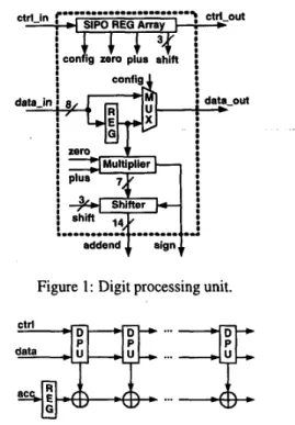
To meet this requirement, a digit processing unit (DPU), as shown in Figure 1, is designed. Control signals are seri- ally shifted into a serial-in-parallel-out (SIPO) register (REG) array
on
the top during the initialization. In each DPU, three control signals, plus, zero, and shift, are derived from the corresponding digit in the z t h tap coefficient, d i , k . 2 - P k . The partial term, di,k.
2-Pk.
a [ n - 21, is evaluated by the multiplier and the shifter. Another control signal, config, controls the multiplexer to select either the buffered or the unbuffered input as the output.By cascading the DPUs, appropriately configuring the multiplexer in each DPU, and summing up the outputs of the DPUs and the accumulated sum as shown in Figure 2, we can implement an FIR filter with variable number of CSDs in each tap. For the last digit of each tap, the multiplexer in the corresponding DPU selects the buffered input as the output. Even though the architecture depicted in Figure 2 can be implemented directly, usually, it is necessary to insert pipeline registers in the filter to achieve reasonable speed performance.
2.2. Reconfigurable FIR Filter Chip
To illustrate the feasibility of the proposed reconfigurable FIR filter architecture, we designed a reconfigurable 8-DPU
i I I data in 1 . :
:
:
!7
I B I I *:
! data-out7
I 0:
:
:
: D *Figure 1: Digit processing unit.
data
...
Figure 2: General reconfigurable
FIR
filter architecture.FIR chip based on Figure 2. Detailed architecture is shown in Figure 3 and is referred to as a processing element (PE). In order to reduce the area and the latency required for im- plementing the addition in the filtering process, eight adders are combined to form a single big adder with nine inputs. With different precision in the output of the DPU (15-bit) and the accumulated sum (24-bit), w e introduce a special sign extension generator. It generates the sum of sign ex- tension bits of 8 DPUs' outputs based on the sign outputs of all DPUs. Finally, the addend outputs of 8 DPUs, the output of the sign extension generator, and the accumulated sum latched in the REG are summed together by an adder. One PE is implemented in the chip so that it is capable of at most 8-digit FIR computation. It is also designed to be cascadable so that the
FIR
filter with more taps can be im- plemented.Figure 3: PE architecture.
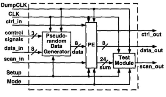
The reconfigurable FIR chip consists of one PE, one pseudo-random data generator
(PRDG),
and one test mod- ule (see Figure 4). There are two clock signals: CLK and DumpCLK, where CLK controls the operating speed of the filter and DumpCLK is used to initialize the chip pa- rameters and to output the results. The parameters in each DPU are pre-calculated based on the filter configuration and then serially shifted into the chip with the ctrl- in signal. Since the chip will be U 0 limited, scan-chain is used for both testing and for normal partial sum communication be- tween cascaded chips. The REG in the PE used to store the accumulated sum is replaced by a 24-bit SIPO register ar- ray. The scan- in signal is used to store the compensation vector explained below for the first chip or the accumulated sum of the previous chip into the 24-bit SIPO serially while cascading. A pseudo-random data generator is designed to provide the input test patterns in high-speed operation. The data fed into the first DPU can be generated by the pseudo- random data generator or data-in signal. Finally, due to the consideration of the output driving capability, a test module accumulates the 24-bit output of the adder in the PE with a 32-bit carry-save adder. The result can be serially scanned out at a slower clock rate to verify the functionality of the chip.Figure 4: Chip block diagram.
3. CIRCUIT IMPLEMENTATION 3.1. Multiplier and shifter
The multiplier is used to multiply the input data x[n - i] by d i , k , which has three possible values: 1, 0, and -1. The operation of each bit can be expressed as
output = zero
+
(plus @ input). (3) If d i , k is 0, the zero signal will be ’1’ and force the output to be 0 regardless of the input. Otherwise, the zero signal will be ’0’ and (3) can be rewritten as output = plus @ input. If the CSD coefficient is 1, the plus signal will be ’1’ and the output is the same as the input. If the CSD coefficientis -1, the plus signal will be ’0’ and the output is equiv- alent to the 1’s complement of the input. The one in LSB that needs to be added to form the 2’s complement negation is accumulated for all negative digits. This sum forms the compensation vector and will be added by setting the initial value of the accumulator.
A shifter is used to multiply the term d z , k
.
z [ n - i] by 2-Pk wherepk E (0,. . .
,7}.
The shifter performs an arith- metic left shift and expands the 7-bit multiplier output (ex- cluding the MSB) into a 14-bit output as the addend signal by shifting the input left by 7 - p k bits. Also, zeros are padded at LSB if the CSD coefficient is ’1’ or ’0’ and ones are padded if the CSD coefficient is ’ - 1’.3.2. Sign extension generator
In our architecture, the accumulated sum is 24-bit wide but the term d i , k
.
z [ n - i] . 2-pk calculated by the DPU is only 15-bit wide (14-bit addend signal and I-bit sign signal). While summing them together, it is unwise to extend each of them to the word length of the accumulated sum. It is better to deal with the sign extension bits separately, so that the area and power consumption can be reduced.A sign extension generator is designed to evaluate the sum of sign extension bits based on eight sign signals. By examining the relation between the number of non-negative sign signals and the sum of the corresponding sign exten- sion bits, a simple implementation of the sign extension generator is designed. The seven most significant bits can
be selected through a MUX by examining if there exists any ’ 1 ’ valued sign signal. If the answer is yes, ’ 11 11 11 1 ’ will be selected, ’0000000’ will be selected otherwise. The three least significant bits are equivalent to the three least signifi- cant bits of the binary representation of the number of non- negative sign signals.
3.3. Adder
The adder is used to sum eight 14-bit addend signals from DPUs, one 24-bit acc signal, and one 10-bit sign- extend signal from the sign extension generator. The acc signal corresponds to the compensation vector or the accumulated sum stored in the REG shown in Figure 3. The acc signal is split into two parts where its fourteen LSBs and eight ad- dend signals are compressed into four 14-bit signals by five 1Cbit carry-save adders in a two-level arrangement. Its ten MSBs are then added with the sign- extend signal and the above four 14-bit signals by a two-level carry-save adder. Finally, an ELM adder [9] modified to reduce the critical path delay is used to compute the final sum.
4. IMPLEMENTATIONS AND MEASUREMENTS Detail circuit design of the reconfigurable FIR filter chip was described in gate level using a hardware description lan-
guage. Functional verification of the circuit design was con- ducted using five filters with different digit configurations. Layout was generated through a standard-cell-based design flow. Functional and timing simulations of the layout were carried out. The final layout is approximately 1.74 x 1.64
mm2 in a single-poly quadruple-metal 0.35-pm CMOS tech-
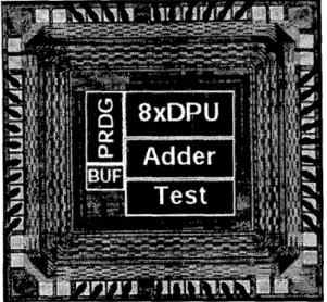
nology and contains 27035 transistors. The die photo of the fabricated reconfigurable FIR filter chip is shown in Figure
5. There are 8 DPUs arranged in one row and three other
blocks: an adder, a pseudo-random data generator, and a test module.
Clock Frequency Power Supply Power Dissipation Process Technologv
Figure 5 : Chip die photo.
86 MHz 2.5 V 16.5 mW 0.35-um 1P4M CMOS The fabricated chip has been tested and its function has been verified. The reconfigurable FIR filter chip can oper- ate correctly at 86 MHz under a supply voltage of 2.5 V and it consumes 16.5 mW. The frequency of the DumpCLK is set to one-fourth of the operating frequency. Table 1 sum- marizes the major features of the reconfigurable FIR filter chip.
Transistor Count Die Size Package
Table 1: Summary of the reconfigurable FIR filter chip.
27K transistors 1.74 x 1.64 mm’
40411 S/B
5. SUMMARY
In this paper, a digit-reconfigurable FIR filter architecture is proposed. The design concepts of the architecture and the circuit are presented. Testing results show that the fabri- cated chip draws only 16.5 mW from a 2.5-V power supply while running at 86 MHz.
6. ACKNOWLEDGEMENT
The authors greatly appreciate the Chip Implementation Cen- ter (CIC) of the National Science Council, Taiwan, R.O.C., for the fabrication and measurement of the proposed chip.
7. REFERENCES
[ 13 J. Mitola, “The Software Radio Architecture,” IEEE Communications Magazine, vol. 33, pp. 26-38, May 1995.
[:2] E. Buracchini, “The Software Radio Concept,” IEEE Communications Magazine, vol. 38, pp. 138-143, Sept. 2000.
[3] R. M. Hewlitt and E. S. Swartzlantler Jr., “Canonical Signed Digit Representation for FIR Digital Filters,” in Proc. of IEEE Workshop on Signal Processing Sys- tems, 2000, pp.416-426.
[4] M. Tamada and A. Nishihara, “High-speed FIR Dig- ital Filter with CSD Coefficients Implemented on FPGA,” in Proc. of the ASP-DAC, 2001, pp. 7-8.
[ 5 ] Y. M. Hasan, L. J. Karem, M. Falkinburg, A. Helwig, and M. Ronning, “Canonic Signed Digit Chebyshev FIR Filter Design,” IEEE Signal Processing Letters, vol. 8, pp. 167-169, June 2001.
[6] T. Zhangwen, Z. Zhanpeng, Z. Jie, and M. Hao, “A High-speed, Programmable, CSD Coefficient FIR Fil- ter,” in Proc. of 4th International Conference on ASIC, 2001, pp. 397-400.
171 K. T. Hong, S. D. Yi, and K. M. Chung: “A High- Speed Programmable FIR Digital Filter Using Switch- ing Arrays,” in Proc. of IEEE Asia Pacific Conference on Circuits and Systems, 1996, pp. 492-495.
181 K. Y. Khoo, A. Kwentus, and A. N. Willson Jr., “A Programmable FIR Digital Filter Using CSD Coeffi- cients,” IEEE Journal of Solid-state Circuits, vol. 31, pp. 869-874, June 1996.
[9] T. P. Kelliher, R. M. Owens, M. J. Irwin, and T. -
T. Hwang, “ELM-A Fast Addition Algorithm Discov- ered by a Program,” IEEE Transactions on Computers,
vol. 41, pp. 1181-1184, Sept. 1992.