Embedded JPEG Encoder IP Core and Memory Efficient Preprocessing
Architecture for Scanner
Chung-Jr Lian, Liang-Gee Chen, Hao-Chieh Chang, and Yung-Chi Chang
E-mail: cjlian @ video.ee.ntu.edu.twDSP/IC Design Lab., Department of Electrical Engineering, National Taiwan University, Taipei, China
Abstract
In this paper; a baseline JPEG encoder soft Intellectual Property ( I P ) is proposed together with a memory efJicient preprocessing architecture for scanner to solve the bandwidth problem between
PC
and scunner. This JPEG IP features that its quantization tables are re-configurable ut run time and compile time. It is a modularized andfully pipelined design with friendly interface, which makes it easier to be integrated into various application systems. It is silicon proven to run up to 4 0 M H z at 3.3V With the optimized preprocessing unit feeding data smoothly into JPEC core, it is a low cost and cotnpetitive solution for scunner to have compression ,function embedded.\
follows. In section 11, the proposed JPEG soft IP is introduced. Then memory efficient architecture for preprocessing unit is described in section 111. Design and simulation results are shown in section IV, and finally the conclusion is given in section V.
"
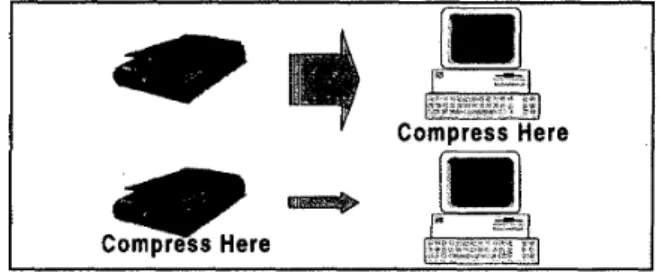
Commess HereFig. 1 Compression inside scanner concept
I.
Introduction
.
While scanning an image, compressing images in the PC side just solves the storage problem, but left the transmission problem between scanner and PC unsolved. Slow scanning speed is now users' chief complaints. As the maximal scan size extends to A3, and the color depth is expected to be 36-bit for color images in the future. The transmission bottleneck between scanner and PC will be more severe. For a A3-size color image with 600dpi, total data will be about 1,600 Mbits (16.54xl1.69x600x600 ~ 3 x 8 ) . Such a large amount of data of just only one image will cost several minutes to transmit. By moving the compression scheme into scanner, 20 to 40 times or even higher time saving is easily achieved with reasonable JPEG [ 11 compression ratio. Compression inside makes a scanner more competitive and will be inevitable in the near future. To implement this idea, either using microprocessor with a large frame memory or integrating a single chip JPEG encoder in the board level is not cost effective. Hence, we proposed a low cost solution based on JPEG IP integration in chip level combining the customized preprocessing circuit.
The remaining parts of this paper are organized as
11. JPEG Encoder Soft IP
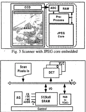
Different from once off design [2], the JPEG encoder soft IP [3] is proposed for reuse. The block diagram of the JPEG encoder IP is shown in Fig. 2 . It is highly modularized and fully pipelined. Interfacing is always the most concerned problem of IP integration. Pixel-level stoppable mechanism is adopted in this design in the view of easy system integration. Compared with block-level processing design [4], it is more flexible and provides a user-friendly interface. Every register in this IP core can stall for any period at any time controlled by the PAUSE signal. PAUSE signal may be enabled due to the bus busy situation, which is very common in real application environment such as a scanner connected to PC. Adopting the policy of separating JPEG core and interface design, input/output buffers with overflow control are considered independently. That makes it easier and cost effective to be customized for different IP users' requirements. To meet different requirements of compression ratio and image quality trade-off, quantization scheme is re- configurable both at compile time and rpn time for user to define different quantization tables.
Fig. 2 Block diagram of the JPEG encoder IP
111. Preprocessing
Unit
A memory efficient preprocessing unit needed for JPEG encoder IP core to be integrated into a scanner is described in this section. In Fig. 3, a functional block diagram of a scanner with an embedded JPEG encoder IP core is depicted, and the proposed architecture of preprocessing is shown in Fig. 4. The preprocessing circuit is responsible for feeding smoothly the JPEG encoder with the proper data. Three main functions are considered in this circuit. They are Line Spacing Re-alignment, RGB-to-YCbCr Color Conversion, and Raster-to-Block Scan Converter. Duc to the low cost constraint of the scanner product, the memory used is expected to be as low as possible. The detail analysis and design of the three functions are in the following subsections.
I
ControlI
Fig. 4 Proposed preprocessing unit architecture
A. Line-Spacing Re-alignment
In a scanner with Charge Coupled Device (CCD) as its sensing elements, there are three linear-array CCD sensors responsible for the sensing of Red(R), Green(G), and Blue(B) color components respectively. Due to the spacing between each linear array, the RGB outputs from CCD are not well aligned. The phenomena with line spacing of 4 and 8 pixels are shown below.
line spacing = 4 :
R1.l >Gs,t, B , , , Rt.2 ,G,2 3 B9.2 ,R1,3’GT,T, B9.q 3
...
line spacing = 8 :
R,,,,G,~,,B17.,’RI.?’G‘),Z’B1,,2’RI,;IG‘),;r B17.;,...-..
(where R,,, ,i is line number, j is pixel number in a line) To re-align these components, i.e. to recover the order into G,,,, B,.,, R,,,, Bl,,
....,
2N lines of B components and N lines of G components have to be buffered until the first line ofR
components of this image are inputted. Therefore, a buffer of size 3Nx(ImageWidth) is needed, where N represents the line spacing.B. RGB-to-YCbCr Color Conversion
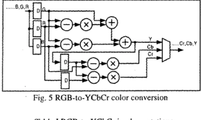
JPEG itself is color blind, but according to the industrial JPEG File Interchange Format (JFIF) [5] specified for interoperability, the color coordinate used should be YCbCr color space. The conversion equations between RGB to YCbCr specified in CCIR 601 are shown below,
Y
=
0.299(R-
G)
tG
t 0.114(8-
G/
Cb
=
0.564
(8-
Y)
t 128cr
=
o . 7 1 3 ( ~-
Y) t 128and it can also be expressed in matrix form below. Y 0.299 0.587 0.1 14][ R ]
-0.169 -0.331 0.500 G
.
[
::4=[
0.500 -0.419 -0.081 BSince the coefficients of the transform are fixed, multiplication can be realized by hardwired multiplier. To implement the conversion, matrix form needs seven hardwired multipliers and two right-shift operations, while direct implementation of the CCIR601 Formulas needs only four hardwired multipliers as shown in Fig. 5. Table I shows the comparisons of different implementations. Compared with the design in 161 and the patent of [7], our design still needs less logic cells. The reason is that both the input and output of RGB-to-YCbGr module are in serial form. Parallel processing of the three components is
not necessary since the memory chosen is only one read and one write in one clock cycle, and the timing constraint in this functional block is not so critical in scanner application. For color images with 2: I sub-sample in both horizontal and vertical, averaging opcration of two adjacent lines is necessary. Therefore, two lines of buffer are needed for this averaging operation, and for pingpong mode switching, another two lines are added. That is, we need totally four lines of buffer for each component.
...B, G
.Cb,Y
Fig. 5 RGB-to-YCbCr color conversion Table I RGB-to-YCbCr implementations
C. Raster-to-Block Scan Converter
Due to the block-based processing characteristics of
JPEG,
there must be a converter to transfer the original raster scan order to block-based order. For gray level images, the Minimum Coding Unit (MCU) defined in JPEG standard is a block (8x8 pixels), and the buffersize
needed is Bx(ImageWidth)x2, where x2 is the result of pingpong mode operation. For color images with 2:1 sub- sample both in horizontal and vertical (4:2:0 format), the MCU consists of four luminance blocks followed by two chrominance blocks. Then, the buffer size needed is 16x(ImageWidth)x2 and 8x(ImageWidth/2)~2~2 for luminance and chrominance, respectively.IV. Design and
Simulation
The overall memory size after the detail analysis and optimization described in section I11 is much smaller than the frame size. That is, it is not necessary to store the
whole image before these preprocessing. The memory size needed only depends on the image width. For line spacing 8,
a
A4-size image at 600dpi (5104-pixel wide) and 4:2:0 format, buffer totally needed is 5 104*84=428,736 bytes, hence a 512kx8 memory is sufficient, The memory map is shown in Fig. 6 conceptually. With a parameterized address generating circuit to generate the required access pattern, it is able to accomplish the three pre-processing functions described above, and feeds the JPEG encoder with preprocessed data smoothly.The overall system is simulated with mis-aligning images shown in Fig. 7 as the input to the preprocessing circuit, then the preprocessed data are sent to the JPEG encoder for compression. The HDL simulation output is a JFIF compatible JPEG file with file header added automatically. It
is
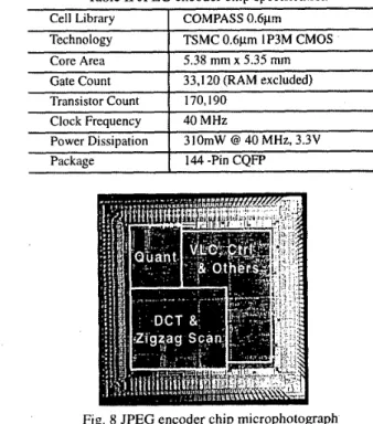
verified by decoding the compressed file through any software decoder available on PC.For silicon verification, the JPEG encoder IP is synthesized with COMPASS 0.6
pm
standard cell library, and fabricated by TSMC SPTM process. The chip specification of this prototype is summarized in Table 11, and the chip microphotograph is shown in Fig. 8.for line
spacing 8
su bsample
for Raster-
to-BlOCk
Fig. 6 Memory map for line spacing 8
R G B
line spacing phenomena (unwanted pixels) Fig. 7 Input with line spacing misalignment
V.
Conclusions
An IP-based JPEG encoder integration with a memory efficient preprocessing architecture for scanner is proposed in this paper. This JPEG encoder IP features that the quantization table is re-configurable, and the whole design is highly modularized, fully pipelined, and with friendly interface, which makes it easier for system integration. The optimized preprocessing unit with low
memory requirement can feed the embedded JPEG IP core wit6 data smoothly. The proposed embedded JPEG encoder IP core with this memory efficient preprocessing circuit is a low cost and competitive solution for scanner to have compression function inside.
Table I1 JPEG encoder chip specification Cell Library Technology Core Area Gate Count Transistor Count Clock Frequency Power Dissipation Package COMPASS 0.6pm TSMC 0.6pm IP3M CMOS 5.38 m m x 5.35 mm ~ 33,120 (RAM excluded) 170,190 40 MHz 3 I OmW @ 40 MHz, 3.3V 144 -Pin COFP
References
[ 11 Iso/IEC, International Standard DIS 109 18, Digital Compression and Coding of Continuous-Tone Still Images.
[2] Marker Peryer, Mentor Graphics, “When dose it make sense to design for reuse,” in Proceedings of the Intellectual Property System on Chip Conference, pp.49-58, March 1998.
[3] Hao-Chieh Chang, LiLin Chen, Chung-Jr Lian, Yung- Chi Chang and Liang-Gee Chen, ”IP Design of a Re- configurable Baseline JPEG Coding”, in Proc. Asia Pacific Conference on ASICs (AP-ASICt99), Seoul, Korea, Auguest, 1999.
[4] Integrated Silicon Systems (ISS), JPEG Encoder Core Datasheet, http://www.iss-dsp.com
[5] Eric Hamilton, C-Cube Microsystems, JPEG File Interchange Format, Version 1.02, September 1, 1992 [6] Kazuya Ogawa, Takashi Urano, Kazuhiko Kondo,
Natsuki Mori, Shinsuke Moriai, Hideyuki Yamamoto, Shin’ichi Kato, Sanyo Elc. Co., Ltd. “A Single Chip Compression/ Decompression LSI Based on JPEG“. IEEE Transactions on Consumer Electronics, August 1992
[7] Rong-Fuh Shyu, Winbond Electronics Corp., “Method and Apparatus for Reducing the Number of Matrix Operations When Converting RGB Color Space Signals to YCbCr Color Space Signals,” US Patent NO. 5 $4 1,422.