ISCAS 2000 - IEEE International Symposium on Circuits and Systems, May 28-31, 2000, Geneva, Switzerland
A Programmable VLSI Architecture for 2-D Discrete Wavelet
Transform
Chien-Yu Chen, Zhong-Lan Yang, Tu-Chih Wang, Liang-Gee Chen
Department of Electrical Engineering, National Taiwan University
1, Roosevelt Road Sec. 4,
Taipei 106, Taiwan
Abstract
Many VLSI architectures for computing the discrete wavelet transform (DWT) were presented, but the parallel input data- sequence and the programmability of the 2-D DWT were rarely mentioned. In this paper, we present a parallel-processing VLSI architecture to compute the programmable 2-D DWT, including various wavelet filter lengths and various wavelet transform levels. The proposed architecture is very regular and easy for extension.
To eliminate high frequency components, the pixel values outside the boundary of the image are mirror-extended as the symmetric wavelet transform and the mirror-extension is realized via the routing network. This design has been implemented and fabricated in a 0.35pm IP4M CMOS technology and the working frequency is 50 MHz. The chip size is about 5200pmx2500pm. For a 256x256 image, the chip can perform 30 frames per second with the filter length varying from 2 to 20 and with various levels. Hence the proposed architecture is suitable for real-time applications such as JPEG 2000.
1.
Introduction
The DWT is a multi-scale frequency analyzer. It decomposes a signal into many subbands with different frequency characteristics. The higher frequency subbands have finer time resolution, and the lower frequency subbands have coarser time resolution. Since it outperforms some traditional time-frequency representations such as the short-time Fourier transform, the DWT has been considered suitable in many image coding applications. But in real-time applications the DWT must operate under high speed, therefore many VLW architectures have been reported to achieve real-time computing and high hardware utilization. Knowles [I] presented a simple 2-D DWT architecture for the case of Daubechies 4-tap wavelet. Later, Parhi [ 3 J proposed two architectures referred to the folded architecture and the digit-serial architecture for I-D and 2-D DWT. Vishwanath [4] improved the performance by means of the linear systolic array, and presented an effcient storage structure. However, few of these papers discussed about the programmability of the DWT such as reconfiguring the filter length. Actually, previous studies are difficult to adaptively modify their data paths to meet various wavelet filter lengths. The proposed architecture uses the routing network torealize the DWT with various filter lengths and various transform levels. Also, most of the previous studies only considered the serial input sequence, however it is very likely to have the parallel input sequence in an embedded system, such as a digital still camera system embedded with a wavelet-based compression engine. Our design methodology, which chooses the parallel processing, is based on the above point of view.
2. Row-Based RPA
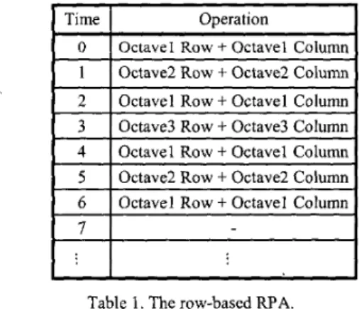
The RPA, which is widely used in the DWT, can not be directly applied to our parallel-processing architecture. Since in our architecture an entire row of the image data must be processed in parallel, we need to schedule an entire row, rather than a single pixel, each time. Therefore the scheduling can be viewed as the I-D RPA [ 7 ] , in which each pixel can be viewed as an entire row of the wavelet coefficients. From the down-sampling characteristic of the DWT, we can see that the number of rows in the higher octave is one half the number of rows in the lower octave. Thus we can intersperse the row operation of various octaves in between the first octave like the I-D RPA. In addition, after each row operation, we can proceed the column operation to generate the wavelet coefficients of an entire row in the corresponding level. If we schedule the row and column operations like the above described, the scheduling will be very simple and straightforward. Table 1 shows the row-based RPA.
Octave2 Row
+
Octave2 Column 23
I
Octavel Row+
Octavel ColumnI
octave3 ROW+
octave3 Column Octavel Row+
Octavel ColumnI I
7
Table 1. The row-based RPA.
It should be noted that only 1/2'"') of the PES operate in the higher octaves, i is the octave index. Although the operations in higher octaves have lower hardware utilization, they also take less processing time ( I D ' of overall processing time). We can estimate the overall hardware utilization:
L
1
leveli-operation-time ,=I overall-operation-time Utilization = (leveli-utilizationx
1 1 1 1 1 1 1 2 2 2 2 2 = l x - + - x T + , x T +...+-
2L-l x- 2 L 2 1 3 4 = -(I - 7) -_ -
2 if L is large 3 0-7803-5482-6/99/$10.00 '2000 IEEE 1-619Compared with the conventional pyramid algorithm, the row-based RPA can reach the same hardware utilization, 66.7%.
3.
Architecture
Considering a 3-level DWT and the filter length is 3, the image data and the wavelet coefficients are shown in Figure 1. The lowest blocks are the image data, while the higher blocks are wavelet coefficients in different octaves and the dash lines illustrate the boundary of the image. The transparent blocks are those required for the operations in the next octave. For an image with 8 pixels (a
4 ) per row (see Figure I), we need 8 processing elements (PES) for parallel processing, and each PE computes one wavelet coeficient in the corresponding column. Those blocks outside the boundary (b and g) are mirror-extended with a and h respectively. Operations in the higher octaves are similar to those in the first octave.
wavelet Coefficient level level 3
Figure 1, Operations of an 8-point wavelet transform. The DWT operations are implemented with the proposed architecture shown in Figure 2. The architecture has five main parts: the PES, the routing network, the memory cells (40 rowsx256~12 bits), the addressing elements and a controller. A PE is shared by
all memory cells (one memory cell stores one bit data) in the corresponding column, i.e. one PE per column. After calculation, the PE stores the wavelet coefficients in the memory cells under them. The detailed function of each part will be given in the following sections.
Controller
40 Addressing Elements
I
....
Roiifing 256 PES Network....
Memory Cells
....
Figure 2. Block diagram of the proposed DWT architecture.
3.1
DWT Operations
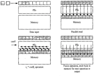
The basic idea of this architecture is to compute the DWT by the SIMD parallel-processing concept with the efficient routing network. The separable 2-D DWT can be divided into two operations, the row and column operations. The whole 2-D wavelet operation is shown in Figure 3. Initially, the input data buffer receives the serial data and prepares for parallel processing. After receiving a whole row, i.e. 256 pixels, it stores them to the memory and the row operation starts. First, the routing network reads a whole row and then dispatches the data to the PES to calculate the wavelet coefficients. The column operation, which is
almost the same for the PES, follows the row operation. The only difference is that during the column operation, the PES get the data in the same column because the data generated by the row operation are stored in the same column but in the different row. After the row and column operations, only the wavelet coefficients in the LL band are stored for the operations in the higher octaves and those in the other three subbands (LH, HL and HH) are output to reduce the storage size.
DEI-
I
PESI
1
MemoryI
1
Memory1
Data input Parallel read
coeff
,
IFinish operation, store back to memory for next operation or
x, * coeff, operation
output
Figure 3. DWT operations.
3.2 Bit-Serial Processing Elements
The PES are the main part of this design for the parallel-processing architecture. They get the image data from the routing network to compute the wavelet coefficients. From the hardware C simulation, the peak signal-to-noise ratio (PSNR) saturates when the word lengths of the intermediate data and the wavelet filter coefficients
are 12 bits wide. Although each PE is responsible for one wavelet
coefficient in a row, a PE’s pitch can only match the total pitch of four memory cells. For the regularity in the full-custom layout, we divide 12 bits into 3 rows and use a 4b (filter coefficient)xlb (data)
MAC instead of a full-precision, i.e. 12bx12b, MAC to compute
the wavelet coefficient by time multiplexing. As shown in Figure 4,
each PE consists of four 1-bit full adders, a 24-bit DRAM buffer, and some logic circuits for the multiplication.
(from ram cache)
a n y
Result
Figure 4. The processing element.
The computing process for a wavelet coefficient is as follows.
where
= y!-'[O]xwo[3: 0]+ y!-'[O]xw,[7: 4]+ y:~'[O]xw,[l I : 8]+
First, complete all LSBs of the data; then proceed to the second LSBs and continue to finish a full-precision MAC operation. It needs 72 cycles to compute an MAC operation and 72n cycles to complete a wavelet coefficient. The clock frequency for a 256x256 image at 30 frames per second is
where n is the maximum filter length of HPF and LPF.
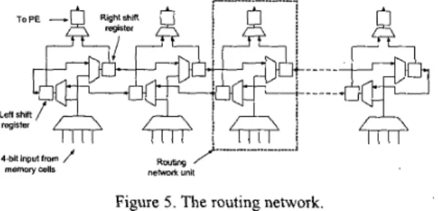
3.3 Routing Network
The routing network is in charge of dispatching the correct data at the right moment to each PE. In the row operation, the routing network reads a whole row of data (256x4 bits) from the memory and provides the PES with the data by two shift registers. Figure 5 shows the architecture of the routing network. Each routing network unit consists of three registers and some multiplexers and there is one routing network unit per column. The connection
between the routing network units forms two shift registers (one shifting right, while the other shifting left). In the beginning of a row operation, all routing network units read one bit data from the memory and transfer it to the corresponding PES to start the computing process. Every time the routing network shifts, the PES can get the neighboring data. The longer the wavelet filter length is, the more times the routing network will shift to get the data required for the DWT. For operations in the higher octaves, the PES will require (2'-')th data away from both sides of the current column and the routing network will shift 2'-' times before the PES
finish the current operation. Although it takes more time to finish a wavelet operation with longer filter length in this architecture, the programmability can be easily achieved.
/
J4-bltmputfmm / P.C.Ub*g
network ""lt
memory cells
Figure 5. The routing network.
Another important issue for the DWT is the boundary problem. To eliminate high frequency components in the boundary of an image, it is necessary to mirror-extend the image data before filtering. The connection in the boundary of the routing network is also shown in
Figure 5 . Since these two shift registers connect like a ring, if the value in the boundary shifts left, it will shift back to the right- shifting registers, and vice versa. Through the connection, it seems that the image data are mirror-extended in the boundary even we don't really extend the image data. We could implement the mirror- extension as long as the filter length is shorter than twice the length o f a row.
3.4 Addressing Elements and Memory Cells
Figure 6. Simplified diagram of the addressing element. For the memory addressing, each row of the memory has an addressing element, which contains a register and some logic circuits as shown in Figure 6(a). The reason we use addressing elements instead of a row decoder is for the programmability and expandability. Owing to the regular data access in the DWT, some shifting operations can afford this job. By programming the addressing elements, we can divide the memory into many memory banks for different octaves. If the filter length is K and the number of octaves is L, the memory cells will be divided into L banks and each bank contains (K+l) rows of the memory, in which K rows
are for the column operation, and one row is for the row operation. If the addressing element is not in the boundary of a memory bank, it will shift down the addressing pointer to the next register as shown in Figure 6(b). Otherwise the addressing pointer will be shifted back to the addressing element in the opposite boundary to form a circular shift register, as shown in Figure 6(c). If an addressing element is activated, the corresponding row of the memory cells will be read or written. While expanding the number o f rows of the memory, we just need to add an addressing element to the left of each row. For the considerations of area and implementation, each memory cell is a 3-transistor (3T) DRAM. The area of a 3T DRAM is less than a half of a 6T S U M , and it is simpler to design than a 1 T DRAM.
4.
Comparison
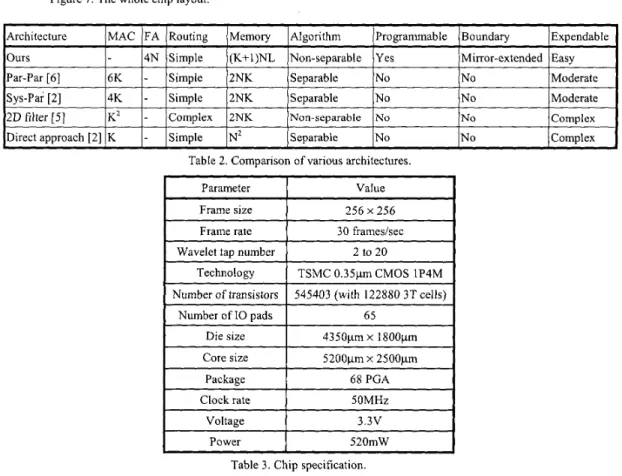
Table 2 lists some of the existing DWT architectures and N is the image size. The proposed architecture doesn't have any full- precision MAC and requires only 4N I-bit full adders to achieve 12bx12b precision. Besides, other architectures require at least K MACS to implement the DWT and their data paths depend on the filter length, so it is difficult for them to compute the DWT with various filter lengths. The characteristic of the programmability in this design is at the cost of the memory utilization and the storage size, but it can compute the DWT with various filter lengths and various transform levels. The boundary problem for the DWT is also important, but most literatures didn't mentioned it before. Using the proposed architecture, the boundary problem is solved by the mirror-extension, which is independent of the filter length, via
the efficient routing network. Since the proposed architecture is very regular, it is easy to extend the PE array and the memory cells for a larger image and more octaves.
5.
Conclusion
In this paper, we have proposed an SIMD-based VLSI architecture to compute the programmable 2-D DWT. This chip contains 256 PES in order to calculate 256 pixels simultaneously. With 40 rows of memory cells, this chip can compute 4-tap 2-D DWT with 8 levels, or 9-tap 2-D DWT with 4 levels, even up to 16-tap 2-D DWT with 2 levels. In the coming standard, JPEG2000, there are various filters suggested and the proposed architecturq can compute the DWT with all suggested filters for different applications. The chip layout is show in Figure 7 and the chip specification is listed in Table 3.
Par-Par [6] Sys-Par [2]
2 0 filter [5]
Addressing Element (full custom)
Figure 7. The whole chip layout.
6K
-
Simple 2NK Separable No No Moderate4K
-
Simple 2NK Separable No No ModerateK2 - Complex 2NK Non-separable No No Complex
References
[ I ] G . Knowles, “VLSI Architecture for the Discrete Wavelet Transform,” Electronics Letters, vol. 26, pp. 1184-1 185, July
1990.
[2] M. Vishwanath, R. M. Owens and M. J. Irwin, “VLSI Architectures for the Discrete Wavelet Transform,’’ IEEE Trans.
on Circuits and Systems-II, vol. 42, no. 5 , pp. 305-316, May
1995.
[3] K. K. Parhi and T. Nishitani, “VLSI Architecture for Discrete Wavelet Transforms,” IEEE Trans. on VLSISystems, vol. 1, no. 2, pp. 191-202, June 1993.
[4] R. M. Owens and M. Vishwanath, “A Very Efficient Storage Structure for DWT and IDWT Filters,’’ Journal of VLSI Signal Processing, vol. 19, pp. 215-225, 1998.
[5] C. Chakrabarti, and M. Vishwanath, “Efficient Realizations of the Discrete and Continuous Wavelet Transforms: From Single Chip Implementation to Mappings on SIMD Array Computers,” IEEE Transactions on Signal Processing, vol. 43, no. 3, pp. 759-771, March 1995.
[6] C. Yu and S. J. Chen, “Efficient VLSI Architecture for Separable 2-D Discrete Wavelet Transforms,” IEEE International Symposium on Consumer Efecfronics, Oct 1998. [7] M. Vishwanath, “The Recursive Pyramid Algorithm for the
Discrete Wavelet Transform,” IEEE Trans. on Signaf Processing, vol. 42, no. 3, pp.673-676, Mar. 1994.
Number of transistors Number of 10 pads
~~~~~~~~
IArchitecture /MAC /FA /Routing /Memory ]Algorithm ~ ~ /Programmable /Boundary ]Expendable)
545403 (with 122880 3T cells) 65
lours
1-
1 4 ~ /Simple l(K+l)NL ]Non-separable /Yes /Mirror-extended /EasyI
Die size Core size 4350pm x 1800pm 5200ym x 2500” Clock rate Voltage Power Frame size 256 x 256 5OMHz 3 . 3 v 520mW
I
Wavelet tau numberI
2 to 20I
I
TechnologvI
TSMC 0.35um CMOS 1P4MI
I I I
I
PackageI
68 PGAI
~ ~ ~ ~ ~ ~ ~ ~~~-
Table 3. Chip specification.