Conduction mechanisms for off-state leakage current of Schottky barrier thin-film
transistors
Kuan-Lin Yeh, Horng-Chih Lin, Rou-Gu Huang, Ren-Wei Tsai, and Tiao-Yuan Huang
Citation: Applied Physics Letters 79, 635 (2001); doi: 10.1063/1.1390325 View online: http://dx.doi.org/10.1063/1.1390325
View Table of Contents: http://scitation.aip.org/content/aip/journal/apl/79/5?ver=pdfcov Published by the AIP Publishing
Articles you may be interested in
Mechanism analysis of photoleakage current in ZnO thin-film transistors using device simulation Appl. Phys. Lett. 97, 163503 (2010); 10.1063/1.3502563
Characteristics of polycrystalline silicon Schottky barrier thin film transistors fabricated using metallic junction source/drain with erbium silicide and platinum silicide
Appl. Phys. Lett. 94, 053502 (2009); 10.1063/1.3073047
Suppression of Schottky leakage current in island-in amorphous silicon thin film transistors with the Cu Cu Mg as source/drain metal
Appl. Phys. Lett. 91, 062103 (2007); 10.1063/1.2767147
Large-area patterning of a solution-processable organic semiconductor to reduce parasitic leakage and off currents in thin-film transistors
Appl. Phys. Lett. 90, 244103 (2007); 10.1063/1.2748841
Excimer laser irradiation induced suppression of off-state leakage current in organic transistors Appl. Phys. Lett. 90, 222103 (2007); 10.1063/1.2743925
This article is copyrighted as indicated in the article. Reuse of AIP content is subject to the terms at: http://scitation.aip.org/termsconditions. Downloaded to IP: 140.113.38.11 On: Thu, 01 May 2014 07:08:04
Conduction mechanisms for off-state leakage current of Schottky barrier
thin-film transistors
Kuan-Lin Yeh
Institute of Electronics, National Chiao Tung University, 1001 Ta-Hsueh Road, Hsin-Chu 300, Taiwan Horng-Chih Lina)
National Nano Device Laboratories, 1001-1 Ta-Hsueh Road, Hsin-Chu 300, Taiwan Rou-Gu Huang, Ren-Wei Tsai, and Tiao-Yuan Huang
Institute of Electronics, National Chiao Tung University, 1001 Ta-Hsueh Road, Hsin-Chu 300, Taiwan
共Received 22 March 2001; accepted for publication 5 June 2001兲
Conduction mechanisms for the off-state leakage in Schottky barrier thin-film transistor were explored. It was found that the field-emission process dominates the leakage conduction of the device with the conventional structure as the field strength in the drain junction becomes high, and results in the strong gate-induced drain leakage共GIDL兲 like phenomenon. In contrast, for the device with a field-induced-drain structure, the high-field region is pulled away from the silicided drain. As a result, the field-emission conduction is eliminated, so the GIDL-like leakage current is effectively suppressed. © 2001 American Institute of Physics. 关DOI: 10.1063/1.1390325兴
Polycrystalline silicon 共poly-Si兲 thin-film transistor
共TFT兲 is an important switching element for large-area
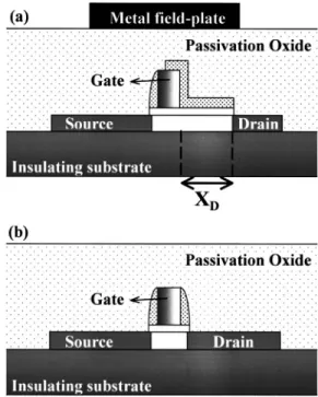
elec-tronic applications, such as active-matrix liquid-crystal dis-play, organic light-emitting disdis-play, etc. For these applica-tions, simple, low-temperature processing, and a high on/off current ratio are very desirable for cost reduction and high performance. In order to meet these goals, we have recently proposed and demonstrated a Schottky barrier thin-film tran-sistor 共SBTFT兲 featuring co-silicided source/drain and field-induced drain共FID兲 extension1,2as is schematically shown in Fig. 1共a兲. The silicided source/drain scheme, which are formed using the conventional self-aligned silicidation tech-nique, saves the ion implantation and associated annealing steps, thus greatly simplifying the fabrication processes, and could also reduce the thermal budget. Meanwhile, the FID feature induced by the subgate 共i.e., field plate兲 enables the device for ambipolar共i.e., p- and n-channel兲 operation. Our experimental results showed that an on/off current ratio as high as 106 for both p- and n-channel operations can be
achieved simultaneously on the same device. More impor-tantly, the gate-induced drain leakage 共GIDL兲 like off-state leakage current encountered in a conventional SBTFT 关i.e., without a field plate, using sidewall spacers to isolate the source/drain and the gate during salicidation, as shown in Fig. 1共b兲兴 could be completely suppressed.2In this work, we further carried out a detailed study on the off-state leakage characteristics of the devices at different temperatures. Based on these results, the conduction mechanisms for off-state leakage are discussed and identified.
Devices were characterized using a HP4156 parameter analyzer. Drain current was measured with gate voltage sweeping from 5 to ⫺5 V. For the p-channel operation, the drain and subgate共i.e., field plate兲 voltages are ⫺3 and ⫺50 V, respectively. While for the n-channel operation, the drain and subgate voltages are 3 and 50 V, respectively. For
com-parison, measurements were also performed on conventional SBTFT shown in Fig. 1共b兲.
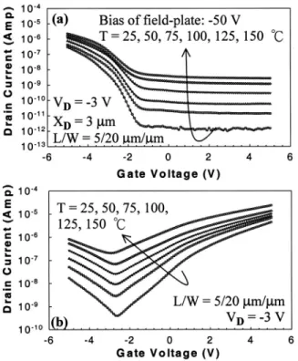
Figures 2共a兲 and 2共b兲 show the typical ID– VG
character-istics under p-channel operation, measured at different tem-peratures, for the SBTFT with FID and conventional struc-tures, respectively. As can be seen in Fig. 2, the conventional SBTFT depicts very poor performance, with intolerably high off-state leakage. In contrast, the on/off current ratio at room temperature is higher than 105 共and could reach 106 if the gate voltage is further increased兲, though it decreases with increasing temperature. In addition, regardless of the tem-perature, the SBTFT with FID is essentially free from the GIDL leakage in the off state, i.e., drain current is nearly
a兲Electronic mail: [email protected]
FIG. 1. Structures for共a兲 SBTFT with a field plate and 共b兲 SBTFT without the field plate are shown. XDin共a兲 is the length of the offset region in the
channel.
APPLIED PHYSICS LETTERS VOLUME 79, NUMBER 5 30 JULY 2001
635
0003-6951/2001/79(5)/635/3/$18.00 © 2001 American Institute of Physics
This article is copyrighted as indicated in the article. Reuse of AIP content is subject to the terms at: http://scitation.aip.org/termsconditions. Downloaded to IP: 140.113.38.11 On: Thu, 01 May 2014 07:08:04
independent of the applied gate voltage. This is in strong contrast with the results of the conventional SBTFT shown in Fig. 2共b兲.
The corresponding Arrhenius plots for FID and conven-tional SBTFTs, measured at VG⫽0 and 4.5 V, are depicted in Fig. 3. The extracted activation energy clearly shows two trends. First, EA for conventional SBTFT is lower than that
of the SBTFT with FID for a given VG. Second, for
conven-tional SBTFT, EA is very sensitive to the gate bias and
de-creases as VG becomes more positive in the off state. In
contrast EA for SBTFT with FID shows only very minor
dependence on VG in the off state. Though the results for
n-channel operation are not shown, similar trends were
ob-served. For example, EA values for n-channel operation of conventional SBTFT are 0.492 and 0.210 eV at VG⫽0 and
⫺4.5 V, respectively. In contrast, the EA values for FID
de-vices fall in the range of 0.56 –0.57 eV in the off state that is nonsensitive to VG.
Based on the aforementioned findings, band diagrams as illustrated in Fig. 4 are proposed to explain the leakage mechanism. In Fig. 4, we concentrate only on the p-channel operation. Similar results could also be deduced for
n-channel operation. For the conventional SBTFT, the field
emission and thermionic emission of electrons from the drain are presumably the two primary conduction mechanisms re-sponsible for the off-state leakage 关Fig. 4共a兲兴, and the two mechanisms are competing with each other. Under the con-dition when the field strength is weak, for example, VG⫽0, the thermionic emission dominates so the activation energy for the leakage will be close to the barrier height. As the potential difference between the gate and the drain (VGD)
increases, the contribution from the field emission will in-crease, owing to the higher field strength. This is evidenced from Figs. 2共b兲 and 3 that EA for the conventional SBTFT
decreases when the off state兩VG兩 increases.
On the other hand, when FID scheme is implemented, as shown in Fig. 4共b兲, the existence of FID will pull the high-field region in the channel away from the drain side. As a result, thermionic emission becomes the major conduction mechanism in the off state so the leakage becomes insensi-tive to VGD关Fig. 2共a兲兴. It is also worthy to note that the high bias applied on the field plate 共e.g., ⫺50 V兲 would shift the Fermi level in the offset channel region closer to the valence band edge, thus raises the barrier height for thermionic emis-sion. This explains why the EA for the device with FID shown in Figs. 2共a兲 and 3 is higher than that of the conven-tional SBTFT.
In summary, we have experimentally investigated the conduction mechanisms of the off-state leakage current for SBTFTs with FID and a conventional structure. The results show that the activation energy of the off-state leakage de-creases significantly with increasing兩VGD兩 for SBTFT with a
conventional structure. This indicates that field-emission FIG. 2. ID– VG characteristics for p-channel operation of SBTFT with共a兲
FID and共b兲 conventional structures characterized at different temperatures are shown. In共a兲 and 共b兲, the current at a fixed VGincreases with increasing
temperature.
FIG. 3. Arrhenius plots for p-channel operation of SBTFTs are shown.
共Empty symbols: FID; filled symbols: conventional structure兲.
FIG. 4. Band diagrams for p-channel operation of SBTFTs with共a兲 conven-tional and共b兲 FID structures are shown (VG⬃0).
636 Appl. Phys. Lett., Vol. 79, No. 5, 30 July 2001 Yehet al.
This article is copyrighted as indicated in the article. Reuse of AIP content is subject to the terms at: http://scitation.aip.org/termsconditions. Downloaded to IP: 140.113.38.11 On: Thu, 01 May 2014 07:08:04
conduction plays a major role as the field strength in the drain junction becomes high, and results in the strong GIDL-like phenomenon. In contrast, the activation energy of the off-state leakage shows only minor dependence on VGD for
SBTFT with FID. This is ascribed to the fact that the high-field region could be pulled away from the silicided drain for the FID structure. As a result, the field-emission conduction will be eliminated, and thus the GIDL-like leakage current can be effectively suppressed.
This work was supported by National Science Council of R.O.C. under Contract No. NSC90-2721-2317-200. The
au-thors would like to thank Dr. G. W. Huang, Mr. Y. M. Deng, and Mr. R. F. Feng at NDL for their assistance and support. The authors are also grateful to Mr. C. Y. Lin for his assis-tance in device fabrication.
1
H. C. Lin, C. Y. Lin, K. L. Yeh, R. G. Huang, and T. Y. Huang, in Technical Digest of the International Electron Device Meeting (IEDM), San Francisco, CA, 2000, p. 857.
2H. C. Lin, K. L. Yeh, R. G. Huang, C. Y. Lin, and T. Y. Huang, IEEE
Electron Device Lett. 22, 179共2001兲.
637
Appl. Phys. Lett., Vol. 79, No. 5, 30 July 2001 Yehet al.
This article is copyrighted as indicated in the article. Reuse of AIP content is subject to the terms at: http://scitation.aip.org/termsconditions. Downloaded to IP: 140.113.38.11 On: Thu, 01 May 2014 07:08:04