國 立 交 通 大 學
電子工程學系電子研究所碩士班
碩 士 論 文
AAO輔助生成一維氧化鋅奈米陣列之特性研究
Characteristics of 1D ZnO Nanowires Array
Grown by AAO Assistance
研 究 生:張家瑋
指導教授:曾俊元
AAO輔助生成一維氧化鋅奈米陣列之特性研究
Characteristics of 1D ZnO Nanowires Array grown
by AAO assistance
研 究 生 : 張家瑋 Student: Chia-Wei Chang
指導教授 :曾俊元 教 授 Advisor: Prof. Tseung-Yuen Tseng
國 立 交 通 大 學
電子工程學系電子研究所碩士班 碩 士 論 文
A Thesis
Submitted to Department of Electronics Engineering & Institute of Electronics
College of Electrical and Computer Engineering National Chiao Tung University
in partial Fulfillment of the Requirements For the Degree of
Master in
Electronics Engineering June 2006
AAO輔助生成一維氧化鋅奈米陣列之特性研究
學生:張家瑋 指導教授:曾俊元 教授 國立交通大學電子工程學系電子研究所碩士班 摘要 本研究以寬能帶(3.37eV)的二六族半導體氧化鋅(ZnO)為主要研 究與探討目標;本實驗將重點著眼於一維方向成長的氧化鋅奈米結 構, 亦即其它兩方向的尺寸限制在100nm以下。另外,陽極氧化鋁 (AAO)結構提供許多優異的特性用於奈米研究上。因此,陽極氧化鋁 提供可控制的一維方向孔洞陣列將是輔助成長奈米線的絕佳利器。 在本研究中,我們將針對AAO輔助生成一維氧化鋅奈米線陣列 的低溫成長方法、化學以及電的特性加以研究探討。此外,我們試圖 探討奈米線的幾何尺寸對於場發射特性的影響。在實驗中,我們利用 低溫的水熱法成長氧化鋅奈米線,而陽極氧化鋁是由傳統的兩步驟陽 極氧化法製備。 事實上,由實驗結果觀察知,奈米線的長寬比與其場發射特性是 成正比關係;在實驗中,當奈米線的長寬比提升到53,我們得到優秀 的場發射特性(β=6100)。最後,對於實驗結果,我發現一些缺點並且 試圖推薦一些修正的可能方法;此外,我們也相信垂直的氧化鋅奈米 線陣列在未來平面顯示器應用上將大有可為,且由水熱法提供的低溫 製程對於可撓式光電與場發射元件的應用也是一大優勢。Characteristics of 1D ZnO Nanowires Array grown
by AAO assistance
Student: Chia-Wei Chang
Advisor: Tseung-Yuen Tseng Department of Electronics Engineering and Institute of Electronics
National Chiao Tung University
Abstract
ZnO is a wide band gap semiconductor (3.37ev) with a large exciton binding energy (60meV) at room temperature, and is one of the most important and versatile semiconductor materials. This research is focus on the one dimension nanostructure of ZnO which indicates the two directions were limited by the nano-scale (smaller than 100nm). The Anodic Aluminum Oxide (AAO) structure would provide some properties for nanotechnology study. Therefore, the AAO which could provide controllable one-dimensional pores was an excellent candidate to assistant fabrication of nanowires.
The characteristics of the ZnO nanowires array by AAO assistance are paying attention in low temperature growth method, chemical and electric properties. Furthermore, we investigate influence on field emission by the geometry scale of nanowire. Here we report for ZnO nanowires growth using the hydrothermal method and AAO prepared by
emitting enhancement factor β is in proportion. For example, the β is enhanced to 6100 which shows excellent field emission when the aspect ratio is 53. In summary, we observed some faults and recommended some improvements. Moreover, we believe that ZnO NWs array grow so vertical that it is a good candidate for the future flat panel display applications, and the hydrothermal method provides a low temperature process for fabricating flexible optoelectronic and field emission devices.
誌 謝
回憶,不停地,在時間的流裡製造著;更不停地,在你我心裡反 覆放映著。 回憶這些日子,實驗室生活也許將只是生命中的一站,但卻令我 成長許多。感謝曾老師俊元教授的指導與教誨,我想在未來旅途中將 受益無窮,更感謝老師提供一個良好的環境給我們無後顧之憂的學習 與成長;亦感謝佳穎學姊與思毅學長不辭辛勞的帶領與教導,秀玉學 姊、群傑學長、志洋學長及昭正學長對於實驗的討論與分析,有了你 們的幫助讓實驗能更順利且更有意義;還有一起努力、成長的信賢與 秉章,真情流露的相互砥礪,讓生活更添感性;以及可愛的學弟們, 冠仲、承佑、鎮宇、重毅、俊勝、俊興、士傑、崧蒔,有你們的協助 與參予,使一切更加美好。 兩年的日子,不長,卻在我心裡留下絢爛的色彩,以及心裡滿滿 的感謝與回憶; 兩年的日子,轉眼間,邁入尾聲,也許我只是各位 曾經協助過我的教授、學長、學弟們人生中的過客,但你們是我生命 中獨一無二的貴人,真感謝你們。 最後更感謝,是敬愛的父母親,默默支持與栽培,無怨無悔;也 是親愛的女友嵐馨,一路伴我走來,分擔憂愁與喜悅,我想這份成果 喜悅亦是屬於你們的。Contents
Abstract Contents... I List of Illustrations ... IV Chapter 1 Introduction ...1 Chap. 1.1 Introduction...1Chap. 1.2 ZnO Characteristics and Nanostructures ...2
Chap. 1.2.1 ZnO Nanowires ...3
Chap. 1.2.2 Synthetic Methods of ZnO Nanowires...6
Chap. 1.2.3 Field Emission and PL Characteristics ...9
Chap. 1.3 Anodic Aluminum Oxide (AAO) & MASK ...13
Chap. 1.4 Capacitance ...22
Chapter 2 Experiment Procedure and Details ...23
Chap. 2.1 Fabrication of AAO and Mask ...23
Chap. 2.1.1 Flow Chart for AAO Fabrication ...23
Chap. 2.2 ZnO with AAO ...27
Chap. 2.2.1 Flow Chart for ZnO with AAO Fabrication..27
Chap. 2.2.2 Fabrication ZnO with AAO ...28
Chap. 2.3 Capacitance ...30
Chap. 2.3.1 Flow Chart of Capacitance...30
Chap. 2.3.2 Fabrication of Capacitance...31
Chap. 2.4 Measurement Equipment ...31
Chap. 2.4.1 Physical Analysis ...31
Chap. 2.4.2 Chemical Analysis ...33
Chap. 2.4.3 Field Emission Detector...34
Chapter 3 Results and Discussion ...35
Chap. 3.1 AAO and Mask ...35
Chap. 3.1.1 AAO ...35
Chap. 3.1.2 Mask ...45
Chap. 3.2.3 XRD Analysis ...66
Chap. 3.2.4 PL Analysis ...69
Chap. 3.2.5 Field Emission Analysis...70
Chap. 3.3 Capacitance ...89
Chapter 4 Conclusions ...90
List of Illustrations
Fig. 1.2-1: (a) It is the fabrication flow of a ZnO NW triode field emission array. (b) the measurement for FE property21... 5 Fig. 1.2-2: It illustrates the mechanism of the photoluminescence. ... 12 Fig. 1.3-1: It illustrates the expansion of aluminum during anodic oxidation.
On the left the level of the un-oxidized metal surface is depicted. ... 15 Fig. 1.3-2: The structure of AAO after anodization. ... 15 Fig. 1.3-3: Relation between anodic voltage with pore diameter of AAO.
... 16 Fig. 1.3-4: The process of the partial electric field in the Al2O3 surface.. 17 Fig. 1.3-5: 1. SEM micrographs of the bottom view of anodic alumina
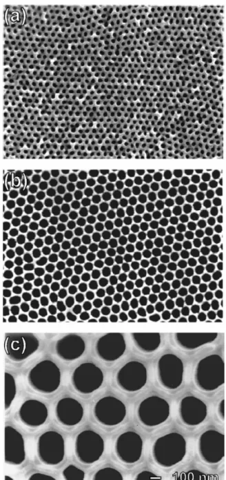
layers. Anodization was conducted in 0.3 M (1.7 wt %) sulfuric acid at 10 °C at 25 V (a), 0.3 M (2.7 wt %) oxalic acid at 1 °C at 40 V (b), and 10 wt % phosphoric acid at 3 °C at 160 V (c). Pore opening was carried out in 5 wt % phosphoric acid at 30 °C for 30 min. (a) 35 °C for 30 min. (b) and 45 °C for 30 min. (c) The thickness of the oxide films was approximately 120 mm. ... 18 Fig. 1.3-6: Lower magnification SEM micrographs of porous alumina
anodized in sulfuric (a), oxalic (b), or phosphoric acid (c). The anodization conditions are the same as those in FIG- 1.3—5.19 Fig. 1.3-7: The high order pore array by FIB lithography... 21 Fig. 1.3-8: The high order pore array by SiC pattern. ... 21 Fig. 1.4-1: It depicts the cross-section of the nonvolatile memory structure and the measurement setup... 22 Fig. 2.4-1: It illustrates the field emission measurement system. ... 34
were without. (4N Al sheet; applied voltage 50V; space of electros: 7; anodic reaction T: 12℃) ... 38 Fig. 3.1-2: 4N Al sheet; annealing 400℃ x 2hrs; applied voltage 50V;
space of electros: 7; reaction T: 12℃... 39 Fig. 3.1-3: The brush-liked AAO was fabricated by over widening
(widened time 100mins). ... 40 Fig. 3.1-4: They were fabricated by conventional two-step anodization. (a) SEM image only by fist step anodize (6, 1), (b) Cross section view. (c) SEM image by two-step anodize (6, 1, 3, 1), (d) Cross section view. (4N Al sheet; annealing 400℃ x 8hrs; applied voltage 40V; space of electros: 7; reaction T: 28℃)... 41 Fig. 3.1-5: They were fabricated by multiple step anodization which was more steps then two-step anodize. (a) SEM image by three step anodize (6, 1, 3, 1, 3, 1), (b) Cross section view. (c) SEM image by four step anodize (6, 1, 3, 1, 3, 1, 3, 1), (d) Cross section view. (4N Al sheet; annealing 400℃ x 8hrs; applied voltage 40V; space of electros: 7; reaction T: 28℃)... 42 Fig. 3.1-6: It was cleaned the residuum on the surface by supersonic shock after multiple step anodize. (a) High magnification (100K) SEM image and (b) low magnification (50K) SEM image revealed the uniform pore array. (4N Al sheet; annealing 400℃ x 8hrs; applied voltage 40V; space of electros: 7; reaction T: 28℃). 43 Fig. 3.1-7: They were fabricated with the same parameters expect
electrolytes. SEM images of the same magnification (100K), (a) was fabricated by 0.3M oxalic and (b) was fabricated by 0.1M H3PO4. (4N Al sheet; annealing 400℃ x 2hrs; applied voltage 40V; space of electros: 7; reaction T: 28℃)... 44 Fig. 3.1-8: AAO template (mask) was fabricated by removing bottom layer
AAO top view of SEM image. (b) The cross section of AAO after removed superfluous Al film. (c) the cross section view of bottom under widening time of 30 mins, (d) the back view of bottom. (e) another one after widening time of 60 mins, (f) the top view. ... 46 Fig. 3.1-9: SEM images about back view of AAO with different reaction time combinations which were different widening and different removing bottom time. (a) total time 100 (70+30) mins, (b) 80 (40+40) mins, (c) 60 (0+60)mins. (widening time, removing time)... 47 Fig. 3.2-1: These AAO were fabricated by two-step anodization (3, 3) on SiO2/Si-sub. (a), (b) were AAO SEM images without widening treatment, porous of diameter was small then 10nm. (c) (d) were widened in 20 mins, porous of diameter was about 30nm. And (d) (e) were widened in 30 mins, porous of diameter was about 50nm. Thickness of AAO was about 1.2μm. (4N Al /SiO2/Si; thickness of Al: 1μm; annealing 350℃ x 8hrs; applied voltage: 40V; electrolyte: 0.3M oxalic; space of electros: 7; reaction T: 12℃) ... 52 Fig. 3.2-2: AAO was fabricated by conventional two-step anodization (3, 3) and widening time was 40mins. (a) It revealed the top view of AAO and many residues on surface. (b) cross section view image revealed the AAO thickness was about 1.2μ. (c) The high magnification (150K) image indicated porous diameter was about 60-85nm, thickness of porous well was about 50 nm and thickness of bottom was about 50 nm. The thickness of porous
... 53 Fig. 3.2-3: AAO was fabricated by conventional two-step anodization (3, 12). They were anodized over suitable time (about 3min) at second anodic treatment. (a) it was widened in 50 mins. (b) it was widened in 80 mins, we observed over winding induced porous wall to break and thickness of bottom to thinner. (4N Al /TiN/Si; thickness of Al: 1μm; annealing 400℃ x 8hrs; applied voltage: 40V; electrolyte: 0.3M oxalic; space of electros: 7; reaction T: 12℃)... 54 Fig. 3.2-4: (a) AAO was fabricated by conventional two-step anodization (3, 12) and widened in 60 mins. Diameter of pores was about 80nm. (b) It was removed the ZnO residues on AAO surface after pores full of ZnO by hydrothermal method. The SEM image revealed the pores full of ZnO successfully. (4N Al /TiN/Si; thickness of Al: 1.3μm; annealing 400℃ x 2hrs; applied voltage: 40V; electrolyte: 0.3M oxalic; space of electros: 7; reaction T: 12℃; ZnO hydrothermal in 2hrs at 96℃) ... 55 Fig. 3.2-5: The AAO full of ZnO was removed AAO in order to form the exposed ZnO NWs. (a). the top view of SEM image revealed island-liked ZnO NWs crowd. (b). the image of cross section view indicated the collapse of ZnO NWs clearly. (4N Al /TiN/Si; thickness of Al: 1.3μm; annealing 400℃ x 2hrs; applied voltage: 40V; electrolyte: 0.3M oxalic; space of electros: 7; reaction T: 12℃; ZnO hydrothermal in 2hrs at 95℃)... 56 Fig. 3.2-6: AAO was fabricated by conventional two-step anodization. The special treatment was supersonic shake to remove residues on surface after widening. (a) Top view. (b)Cross-section view and (c) was high magnification (250K) image of the bottom area.
applied voltage: 40V; electrolyte: 0.3M oxalic; space of electros: 7; reaction T: 12℃) ... 57 Fig. 3.2-7: AAO was fabricated by two-step anodization. The top-view
SEM images were the same magnification, (a) employed 5N Al source and (b) employed 4N Al source. We could clearly observe the improvement of reduced impurities on the surface due to high concentration of Al film. ... 58 Fig. 3.2-8: SEM images of cross section(a),top view(b)(c) Temperature not high enough to assist ZnO migrated into pores, so we observed the ZnO covered the surface and would not full into the porous.(b) 30 mins at 80℃,(c) 1hr at 80℃. The inset in (a) was the high magnification SEM image. ... 59 Fig. 3.2-9: SEM images of cross-section view (a)(b)(c) were different
applied voltage to anodize according to 30V, 40V, 50V. (d), (e), and (f) were reveled different widening time form the sample of (c), and the widening time was 10 mins, 20 mins, 40 mins, respectively. (5N Al /TiN/Si; thickness of Al: 850nm; annealing 400℃ x 2hrs; electrolyte: 0.3M oxalic; space of electros: 7; reaction T: 12℃)... 60 Fig. 3.2-10: (a), (c) are the SEM images of top view, and (b), (d) are SEM images of cross-section view. (a), (b) are fabricated by convectional two-step anodization.(1, 3.5) (c), (d) are widened in 60 mins, the diameter become about 80 nm from 10 nm. (5N Al /TiN/Si; thickness of Al: 500nm; annealing 400℃ x 2hrs; applied voltage: 50V; electrolyte: 0.3M oxalic; space of electros: 7; reaction T: 12℃) ... 61
/TiN/Si; thickness of Al: 1500nm; annealing 400℃ x 2hrs; applied voltage: 50V; electrolyte: 0.3M oxalic; space of electros: 7; reaction T: 12℃; widening time 20) ... 62 Fig. 3.2-12: The TEM cross-section image of AAO full of ZnO prepared by FIB; ; the porous diameter is about 80nm after 40mins widening treatment; the structure is AAO/SiO2/Si-sub... 64 Fig. 3.2-13: (a) TEM image of ZnO NW prepared by supersonic shake
treatment; (b) SAED of ZnO NWs.(c) EDS of ZnO NWs. .... 65 Fig. 3.2-14: It reveals XRD patterns of Al film with different annealing
treatment on TiN/Si-sub., and compares with (a) different annealing time and temperature, (b) RTA... 67 Fig. 3.2-15: It reveals XRD patterns of AAO full of ZnO on SiO2/Si-sub., and compares with (a) annealing (400℃ 2hr) and (b)without annealing... 68 Fig. 3.2-16: It reveals the with Xe lamp as an excitation source (320 nm) at room-tempurature. ... 69 Fig. 3.2-17: Field emitting J-E curve and ln(J/E2)-1/E curve... 71 Fig. 3.2-18: It illustrates operation region of field emission. ... 71 Fig. 3.2-19: The SEM images reveals the morphology of sample B2. It was AAO full of ZnO by hydrothermal in 2.5 hrs at 95℃... 72 Fig. 3.2-20: It shows field emission J-E curve and F-N plot of sample B2. The table shows the detail data... 73 Fig. 3.2-21: It shows field emission J-E curve and F-N plot of sample B2 under a 30W lamp. The table shows the detail data. It indicates the photo-enhanced field emission characteristic... 74 Fig. 3.2-22: The SEM images reveals the morphology of sample C1. It was AAO full of ZnO by hydrothermal in 2.5 hrs at 95℃ and removed the surplus ZnO on the AAO surface. And
Fig. 3.2-23: It shows field emission J-E curve and F-N plot of sample C2. The table shows the detail data... 76 Fig. 3.2-24: It shows field emission J-E curve and F-N plot of sample C2 which was improved by annealing (with 400℃ at 2hrs). The table shows the detail data. ... 77 Fig. 3.2-25: It shows field emission J-E curve and F-N plot of sample
ASS6.4. The table shows the detail data. And length/diameter is 1600/70-80nm... 81 Fig. 3.2-26: It shows field emission J-E curves of different aspect ratio and fixed the diameter. ... 82 Fig. 3.2-27: (a) Turn on field versus NW length, and (b) FE-β versus
Different NW length... 83 Fig. 3.2-28: Active region for Different NW length (fixed
diameter=80nm).Length (um):ASS1.4=0.5, ASS11.3=1, ASS6.4=1.6, Cb=0.6, ASS5.1=1.2. ... 84 Fig. 3.2-29: Active region for Different NW length fixed the diameter. . 85 Fig. 3.2-30: FE for Different NW diameter fixed length (L=500nm).
Diameter (nm): ASS1.4 = 80, ASS1.2 = 30. ... 86 Fig. 3.2-31: FE for Different NW diameter fixed length ( L=1600nm).
Diameter (nm): ASS6.4 = 80; ASS6.2 = 30 ... 87 Fig. 3.2-32: FE-β versus Different aspect ratio. ... 88 Fig. 3.3-1: SEM images of cross-section view (a), top-view(b)(c). (d) was illustration of capacitance measurement. (a) reveales the AAO full ZnO. (b) reveales few ZnO residues on the surface. The partial circle in the image (c)was the top electrode... 89
Chapter 1 Introduction
Chap. 1.1 Introduction
Recently, the nanotechnology have been extensively researched, which contains many kinds of different dimensional nanostructures. For example, there are one dimensional (1D) nanostructure, such as nano-tubes1,2,3, nano-wires4 and nano-rods5,6,7; two dimensional (2D) nanostructure, such as nano-sheets8,9, nano-planes and nano-discs; three dimensional (3D) nanostructure, such as nano-dots10 , 11. The above- mentioned are great importance in studying the physical and chemical properties of nano-materials or constructing functional nano-scale devices, which have been investigated in the potential applications of photonic, electro-optical and electronic device. For example, some applications of different kinds of nanostructures were extensively studied, including to nanodot for nonvolatile memory (nano-crystal memory device, IBM, 1995), nanosheet for solar cell, nanowire for field emission12 and photofluorescent device, etc.
About the studies of one dimensional (1D) nanostructure were quite popular, since the first discovery of carbon nanotubes (CNTs) that were fabricated in 199113. Considerable effort of CNTs has been devoted to the synthesis and characterization of nanoscale. Because of their attractive physical properties enable them to play a major role in nanoscale electronic and nanoscale devices, large studied about CNTs was published. Moreover, many materials were researched to replace carbon in order to improve some insufficient effects of CNTs. So, expect for carbon, a novel material,
ZnO, was attractive and utilized for nanostructure.
The subject was focused on the characteristic and fabrication of 1D ZnO nanostructure. The particulars will be discussed at following sections.
Chap. 1.2 ZnO Characteristics and Nanostructures
ZnO is a wide band gap semiconductor (3.37ev) with a large exciton binding energy (60meV) at room temperature, and is one of the most important and versatile semiconductor materials. Previous studies were investigated into its optical and electric properties14, as well as its ferromagnetic, transparency, photoconductivity, piezoelectric, field emission12, , and light-emitting properties. Further, ZnO has attracted much attention since possible applications in phosphors, transparent conducting films for solar cells, ultra-violet (UV) laser devices15 and flat panel displays were suggested16,17,18.
Since the first report of ultraviolet lasing from ZnO nanowires19, nanostructure of ZnO has stimulated intensive research. Indeed, ZnO nanostructures are interesting to study not only the property of UV lasing emission in nanowire form, but also because a wide variety of morphologies have been prepared. Some kinds of the ZnO nanostructures contain nanowire, nanorod, nanosheet, nanoribbon, nanotube, nanoplate, tetrapod, and flower-liked20 structures. Indeed, based on the nano-scale
Furthermore, the ZnO nanowires are believed to be a viable candidate which compare to CNTs for field emission device, due to its excellent thermal and chemical stability. So, about the prominent properties and the synthetic methods of ZnO nanowires we are interested will be discussed in next sections.
C
Chhaapp..11..22..11 ZZnnOO NNaannoowwiirreess
To come back to the subject, the focus is the 1D ZnO nanowires. The nanowire array is the major structure to investigate; contrary, the signal nanowire was no more attraction as nanowire array, and the main causes were fabricated hardly and applied restrictedly.
To continue mention of Chap. 1.2 , the applications of the ZnO nanowires were focused on the properties of photoluminescence and field-emission (the mechanisms would be discussed at Chap. 1.2.3 ), due to its excellent thermal and chemical stability. There are some qualitative and specific factors for measurement and analysis objectively. About factors of metrical, there are work function and square resistor, etc; about factors of morphology is such as aspect ratio, number density and surface roughness.
We will cit some instants and illustrate some applications at following contents:
1. nanowires array
In particular, exploration of the materials for flat panel displays has been a hot topic for the last few decades. So, current trends in
nanotechnology and nanomaterials play an important role in the potential applications. Then, high aspect ratio one-dimensional (1D) nanostructures, such as nanotubes, nanowires and nanobelts, have been extensively studied with a view to use in vacuum microelectronic devices, including field emission displays (FEDs), electron sources, microwave devices and high power rf amplifiers, because of the advantage of the low turn-on electric field and high electron emission efficiency12.
Recently, ZnO nanowire emitters have been reported to exhibit good emission properties with high stability, low threshold electric field, high emission current density, good emission stability and durability. The ZnO NWs have been synthesized by various procedures (we will discuss in next section); however, the main challenge in fabricating the nanowire based FED devices is the high synthesis temperature which retards the integration processes for FED device structures. A hydrothermal method would offer a superior route for FED fabrication because of the catalyst-free growth, low cost, low reaction temperature, large area and uniform production, environment friendliness and process compatibility with VLSI. As above advantages, the hydrothermal method for low temperature was applied in our works.
2. Field emission triode21,22
Basing on nanowire array, the ZnO NW triode shows good and controllable emission properties with the turn-on anode electric field,
density higher at the same turn-on electric field which compared with one without applying gat structure.
However, the main advantages for the nanowire based field emission device (FED) are a large area display, high uniformity, high productivity, high brightness, low cost, low power consumption and reliability. From this point of view, triode-type FED devices with low driving voltage, high resolution and controllable electron emission characteristics are candidates for constituting a new generation of FED devices. Fig. 1.2-1illustrates the fabrication flow of a ZnO NW triode field emission array.
Fig. 1.2-1: (a) It is the fabrication flow of a ZnO NW triode field emission array. (b) the measurement for FE property21.
3. Doped ZnO nanowires18
We can study the variation and effect on the photoluminescence and field-emission properties by doping the different elements into ZnO nanowire. Farther, we can modulate those characteristic to satisfy with application actuality. For example, Norton and co-workers have reported that the P0.02Mg0.1Zn0.9O film showed stable p-type behavior by adding Mg
and P together—doping with Mg to increase the band gap and P to introduce the acceptor level23’24.
Moreover, such suitable doped NWs exhibit better field-emission properties including the lower threshold electric field, lower resistance in series, and higher emission current density, in comparison with undoped NWs. The improved field-emission characteristic is attributed to the changes in surface state of the nanostructure at both threshold voltage and F-N field-emission regions. Furthermore, the modulated band gap can be obtained with suitable doping, which may also be able to be applied for the future enanohomojunction optoelectronic and field-emission devices.
C
Chhaapp..11..22..22 SSyynntthheettiiccMMeetthhooddss ooffZZnnOO NNaannoowwiirreess
Synthesis methods of ZnO nanostructures can be achieved by various techniques, for example, including as vapor-liquid-solid (VLS) growth12, metal-organic vapor phase epitaxy (MOVPE) procedures, physical
synthesis techniques employed some general semiconductor process machinery equipments, classed like as chemical vapor deposition (CVD), physical vapor deposition (PVD), electrical gun evaporation, thermal evaporation, high temperature chamber, etc. Those synthesis techniques look like similar for results. But, there were some different advantages and handicaps during some procedures. We focused on those handicaps which were fatal; some handicaps of physical property can not be overcome and endured for some applications, which for some materials, such as polymer substrates, will be melted due to high temperature treatment.
Consequently, one of the most serious handicaps to fabricate the nanowire is the high synthesis temperature, which will restrict the selection of substrate materials, even affect integration procedures. Thus, the main challenge in fabricating the NW based FED devices is the high synthesis temperature which retards the integration processes for FED device structures.
Particularity, the hydrothermal method offers a superior route for FED fabrication because of the catalyst-freegrowth, low cost, low reaction temperature, large area and uniform production, environment friendliness and processcompatibility with VLSI.
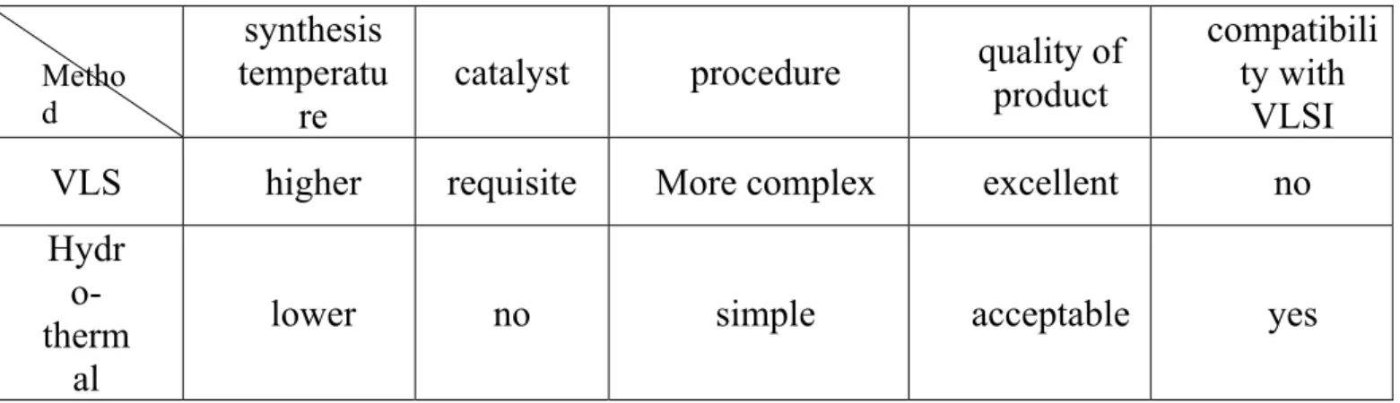
Farther, following discussion was about the comparison of VLS with hydrothermal method, and listed the difference in their detail process and certain limits.
First, the main deficiency in VLS process was the high synthesis temperature (750-950 )℃ . And, the synthesis temperature of hydrothermal
method was low than 100 .℃ However, the high temperature would provide well aligned array and excellent structure oppositely, such as high quality and high aspect ratio.
Another notable difference of VLS with hydrothermal method was the catalyst. For example, the VLS employ Cu (copper) or Au (gold)12,25 as catalyst for growth ZnO. And, the intrinsic properties of catalyst, such as surface morphology and large different of lattice parameter with reaction elements, would cause to variation different of product. Following the example12, the surface of the Cu catalyst film has many ordered square and hexagonal Cu island structures and the lattice parameter of Cu (a=3.215 Å) is close to that of the ZnO (a=3.253 Å). Consequently, the ZnO nanowires can vertically grow from Cu catalyst layer on the Si substrate with VLS, rather than grow from Au catalyst layer. However, the hydrothermal method was always catalyst-free. Generally, the VLS process was complex than hydrothermal method in many particulars, such as flow ratio of carrier gas would obviously effect the product of VLS process.
However, we identify the VLS process was more complex than hydrothermal method. But, we also can not disregard the advances of VLS process. We could select suitably and search the balance according to our applications.
Following would list in Tab.1.2-1 about the comparison between VLS process and hydrothermal method.
Tab. 1.2-1: It shows details of comparison between VLS process and hydrothermal method.
C
Chhaapp..11..22..33 FFiieellddEEmmiissssiioonnaannddPPLLCChhaarraacctteerriissttiiccss
◎ Field emission
In brief words, the field emission is a point discharge phenomenon. It was easily occurred at a long and sharp rod liked needle. When we applied a negative voltage on it, the tip would exhibit a large electric field then other parks naturally. If the applied filed is large enough, the potential barrier would narrow and an appreciable number of electrons at the Fermi level can tunnel through. We set a grounded probe or plant in a suitable distance between with the tip to receive would emit electrons from the tip. So we could constitute measurement equipment illustrated at Fig- 2.4-1, and we could measure the current I (a current passed by probe or plant) and calculate the current density (J) that was I divided by A (area of the probe or plant).
However, this point discharge phenomenon we observed was not sure
Metho d
synthesis temperatu
re
catalyst procedure quality of product
compatibili ty with
VLSI
VLS higher requisite More complex excellent no
Hydr o- therm
al
of field emission; we must check some properties to fit some conditions of the field emission mechanism. We could demonstrate by utilizing those discharge properties fitted the Fowler-Nordheim (FN) equation. The simple mode was that making sure the curve which was the relationship between J and E (applied voltage divided by the emission distance) to fit the F-N relationship. the FN relationship is as follows:
※Fowler-Nordheim (FN) equation:
J = (Aβ2E2/Φ) exp(-BΦ3/2 /βE)
A=1.56x10⁻¹⁰ (AV-2eV) ; B=6.83x10³ (VeV-3/2μm-1)
Where J is the current density, E is the applied field, Φ is the work function of the ZnO (4.45 eV), β is the field enhancement factor, and A, B are constants, A = 1.56 × 10⁻¹⁰ (AV−2 eV) and B = 6.83 × 10³ (V eV−3/2 μm−1)9.
※The field emitting enhancement factor, β:
m=BΦ3/2d/β; m=slop → β= BΦ3/2/m
where the value of β can be calculated from the slope of the F–N plot. The calculated β value would determine the field emission was good or not. Thus, large β value represented a well field emission mechanism; contrariwise small β value meant a poor field emission mechanism. And
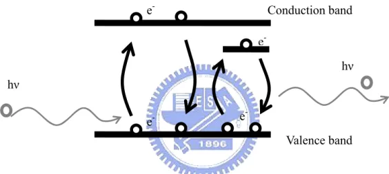
◎ Photoluminescence (PL)
The photoluminescence analysis was a simple physical mechanism which was illustrated in Fig. 1.2-2. In brief statement, about the mechanism of photoluminescence was an energy transport. Generally, the excitation source was some kinds of lamps which could emit different wave length. Different lamp which was filled of different gas would manage to provide a limited range of wave length. For example, we could employ two different kinds of lamps to provide a wide range of wave length. As we know, different metrical absorb particular wave length to provide energy for electron. If electron obtained enough energy, it would be transition from low energy level to high energy level; then, it would release energy when it transit to low energy level. The energy could be released by two type of light: one was excitation, another was emission. And, if the released light was classified according to wave length, it could class as fluorescence and luminescence.
To take a point of ZnO NW array, a photoluminescence analyzer with Xe lamp as an excitation source (~320 nm) was used for optical studies at room temperature. The major photoluminescence peak was the ultraviolet (U.V.) emission which was due to band-edge emission of ZnO, and it could detect different peak. In many studies, those peaks at special wave lengths for ZnO were reported to be caused by the Zn vacancy, oxygen deficiency, deep level, or singly ionized oxygen vacancies, etc. In other words, those
defects of product would cause different energy states excited in the bend-gap. So, those minor peaks would suggest that the produce excited defects.
Fig. 1.2-2: It illustrates the mechanism of the photoluminescence. hν e -e -e -hν Conduction band Valence band e
-Chap. 1.3 Anodic Aluminum Oxide (AAO) & MASK
Anodic Aluminum Oxide (AAO) ◎
The Anodic Aluminum Oxide (AAO) structure would provide some properties for nanotechnology study, which including high ordered density of pores, controllable diameter and length of pores, large area and high uniform, stable chemical property of product, etc. As the result, recently, the AAO applications in nano-scale were studied extensively. Because of the one-dimensional nano-materials exhibit interesting properties, the AAO which could provide controllable one-dimensional pores was an excellent candidate to assistant fabrication.
Generally, the AAO structure was fabricated by a conventional two-step method. From the previous literature29, the two-step was classed as 1.as-perpared pore formation and 2.stable porous growth.
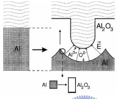
The interaction mechanisms were illustrated at Fig. 1.3-1. Pores grow perpendicular to the surface with the equilibrium of field-enhanced oxide dissolution at the oxide/electrolyte interface and oxide growth at the metal/oxide interface. While the latter is due to the migration of oxygen containing ions (O2-/OH-) from the electrolyte through the oxide layer at the pore bottom, Al3+ ions which simultaneously drift through the oxide layer are ejected into the solution at the oxide/electrolyte interface. The fact that Al3+ ions are lost to the electrolyte has been shown to be a prerequisite for porous oxide growth, whereas Al3+ ions which reach the oxide/electrolyte interface contribute to oxide formation in the case of barrier oxide growth. A possible origin of forces between neighboring
pores is therefore the mechanical stress which is associated with the expansion during oxide formation at the metal/oxide interface. Since the oxidation takes place at the entire pore bottom simultaneously, the material can only expand in the vertical direction, so that the existing pore walls are pushed upwards. Under usual experimental conditions the expansion of aluminum during oxidation leads to less than twice the original volume, since Al ions are mobile in the oxide under the electric field, so partly the oxidized aluminum does not contribute to oxide formation. In experiments, we could observe the relative thickness of the porous alumina layer compared to the consumed aluminum was found to vary with applied voltage and electrolyte concentration.
Following list showed the main chemical reactions of AAO:
Al(s) → Al3+(oxide) + 3e- ...[eq. 1]
3/2H2O(l) → 3H+(aq) + 3/2O2-(oxide) ...[eq. 2]
1/2Al2O3(s) + 3H+(aq) → Al3+(aq) + 3/2H2O(l) ...[eq. 3]
3H+(aq) +3e- → 1/2H2(g) ...[eq. 4]
The AAO cross-section structure after conventional fabrication was illustrated at Fig. 1.3-2. We could control the porous diameters by utilizing chemical etching to widen the pore.
Fig. 1.3-1: It illustrates the expansion of aluminum during anodic oxidation. On the left the level of the un-oxidized metal surface is depicted.
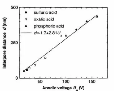
The Fig. 1.3-3 revealed direct proportion between anodic voltage with porous diameter of AAO; when the applied voltage was increase, the porous diameter would increase, and no matter what kinds of electrolyte. The main cause was the applied voltage formed a field-enhance porous reaction. By the way, we obtain different porous diameter at the same applied voltage in different electrolyte.
Fig. 1.3-3: Relation between anodic voltage with pore diameter of AAO30.
The mechanism details of as-prepare pores were shown in the Fig. 1.3-4. The partial electric field would become more concentration in the Al2O3 surface when the applied voltage was increased gradually. Those
partial area would higher reaction ratio (the field-enhance oxide dissolution at the oxide/electrolyte interface and oxide growth at the
The Al3+ and O2+ were combined to form Al2O3 in the surface.
Simultaneously, it would dissolve in the electrolyte due to that the as-prepare pores areas had higher concentrative voltage and higher reaction ratio (those complex ion interactions were discussed at above content). Further, we obtained the Al surface formed the vertical porous array after the second anodic step.
Fig. 1.3-5: 1. SEM micrographs of the bottom view of anodic alumina layers. Anodization was conducted in 0.3 M (1.7 wt %) sulfuric acid at 10 °C at 25 V (a), 0.3 M (2.7 wt %) oxalic acid at 1 °C at 40 V (b), and 10 wt % phosphoric acid at 3 °C at 160 V (c). Pore opening was carried out in 5 wt % phosphoric acid at 30 °C for 30 min. (a) 35 °C for 30 min. (b) and 45 °C
Fig. 1.3-6: Lower magnification SEM micrographs of porous alumina anodized in sulfuric (a), oxalic (b), or phosphoric acid (c). The anodization conditions are the same as those in Fig. 1.3-5.
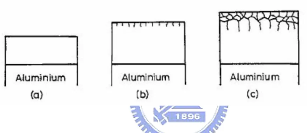
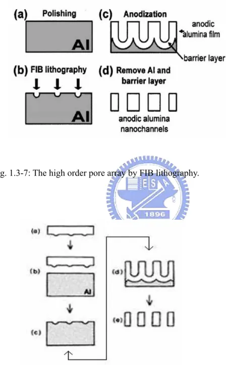
◎ MASK
After the two step process, the main structure was AAO on Al sheet or substrate. The mask was fabricated by etching treatment for removing the film under AAO. Removing the redundant Al sheet and barrier layer was by the different selectivity of etching treatments. We would obtain a nano-channel array look like meshed thin film. It could be employed as mask to fabricate nanotube or nanowire if we widened the porous diameter to achieve suitable scale.
However, the as-prepared pore would determine the further porous properties; however, the as-prepared pore would defined by first anodic procedure, electrolyte, and experiment condition. Hence, some methods were reported in order to improve this question. For example, we could utilize FIB lithography or SiC hard mask to parent the required nano-scale porous array. Those methods were illustrated at Fig. 1.3-8. Although it could achieve the high ordered pore, the process became more complex.
Fig. 1.3-7: The high order pore array by FIB lithography.
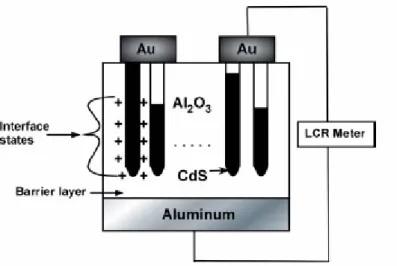
Chap. 1.4 Capacitance
Based on the AAO porous template, one material was deposited on it as electrode. The dielectric was the compound of one metrical with alumina. To control the quality of nano-scale structure was a challenge. It always had large current leakage due to the not well crystalline of alumina.
If we focused on the high interface of AAO, the major point was the contact of material and the porous anodic alumina films, it would exist a large contact surface between material and alumina in the pores. The interface would provide some kinds states. The quality of the interface states would dominate the electric behavior. And the best quality might be employed to applications of memory. In the previous report32, 33: cadmium sulfide (CdS) nanowires of 10nm diameter, electrodeposited in porous anodic alumina films, exhibit an electronic bi-stability that can be harnessed for nonvolatile memory. The current–voltage characteristics of the wires show two stable conductance states that are well separated and long lived. The structure was illustration in Fig. 1.4-1.
Fig. 1.4-1: It depicts the cross-section of the nonvolatile memory structure and the measurement setup.
Chapter 2 Experiment Procedure and Details
Chap. 2.1 Fabrication of AAO and Mask
CChhaapp..22..11..11 FFlloowwCChhaarrttffoorrAAAAOO FFaabbrriiccaattiioonn
Enough reaction time (Al 100% reaction to Al2O3)
Si wafer clean
Barrier layer coat clean
Al layer coater
Al annealing
AAO
AAO tmplate/TiN/Si-sub
Widen the pores diameter
XRD crystalline PL optics SE TE XR crystalline crystalline HR.SAE
C
Chhaapp..22..11..22 FFaabbrriiccaattiioonnPPrroocceedduurreeooffAAAAOO
As-prepared procedure was RCA clean for p-type Si-substrate (100). For barrier the follow-up thermal treatment, we employed TiN thin film as barrier layer, and deposited it on Si substrate by DC sputter in N2
atmosphere, and in vacuum chamber (1X10⁻⁶ Torr). Moreover, the barrier layer provided with conductivity to play a role of sub-electrode. For the prepared AAO template, Al thin film of required thickness was first deposited on the Si wafer by thermal evaporation in vacuum chamber (<5X10⁻⁷ Torr). The purity of Al source was 5N (99.999%) ingots of Al. annealing the Al thin film on TiN/Si-sub at 350-500℃ was in order to release mechanical stress and enhance the crystallization quality. As we knew, the porous morphology of AAO depended on the quality of Al.
The two step anodic procedure, which has been reported in detail elsewhere, was employed to prepare high order porous channel arrays of AAO. Following, the major procedure would list simply. First anodic treatment was carried out in a 0.3M oxalic solution(H2C2O4) at 12℃ and
applied a constant polarization voltage for a few time. The produce was a thin nano-porous AAO in the top surface. Then, we removed the thin nano-porous film by wet chemical etching with a mixed solution of H3PO4
and CrO3 at 60℃, and therefore the surface on the Al film was exhibited a
relatively ordered indent pattern. The indent pattern was the as-prepared porous pattern and determined the surface morphology of AAO channel
However, the existing porous diameter was not wind enough. The pore diameter of the AAO template was widened in a 5% H3PO4 solution for a
widened time.
The mechanism of two step anodic procedure was displayed at ch1-3, and the surface morphology and initial porous diameter were mainly determined by applied polarization voltage and electrolyte. Among of every electrolyte of AAO which were reported in previous literature, the reaction was carried out and based on acid solution, including chromic acid (CrO3), sulfuric acid (H2SO4), oxalic acid (H2C2O4), boric acid(H3BO3), or
phosphoric acid(H3PO4). Those acid solutions were controlled to effective
reaction by different solution concentration and reaction temperature. Actuality, we achieved the porous length and diameter that we ordered by controlled the reaction time and widened time, when we fixed the parameter such as applied polarization voltage, space of electrodes, reaction temperature and electrolyte. The structure of result was AAO template on barrier layer of TiN and substrate of Si (AAO/TiN/Si).
C
Chhaapp..22..11..33 FFaabbrriiccaattiioonnPPrroocceedduurreeooffMMaasskk
For the preparation of the AAO mask, an Al sheet of about several mm in thickness was employed and replaced the Al thin film on TiN/Si-sub in the above process. The Al sheet was passed through the same process flow as fabrication procedure of AAO, such as annealing, two step anodic treatment, and widened treatment. The structure of result was AAO on Al sheet, and we must remove the unnecessary Al sheet first. Further, we removed the bottom (barrier layer) of AAO according to chemical etching in H3PO4 for removed time. At least, the product was the
Si wafer clean
Fill ZnO into the pores
Widen the pores diameter
(Annealing for ZnO with Al2O3)
Remove AAO template Remove ZnO on the AAO surface
High order ZnO NW array
Chap. 2.2 ZnO with AAO
CChhaapp..22..22..11 FFlloowwCChhaarrttffoorrZZnnOOwwiitthhAAAAOO FFaabbrriiccaattiioonn
(Ellipses was listed in chap 2.1.1)
PL I-V FE optics SE TE XR crystalline crystalline HR.SAE
C
Chhaapp..22..22..22 FFaabbrriiccaattiioonnZZnnOOwwiitthhAAAAOO
As the references of ch1-2-2, there were some main methods that could synthesis ZnO. Through by considering and testing, we choose the hydrothermal method from others. At present, one of the most serious points to fabrication was the synthesis temperature. The physical limit of material was too high temperature to apply to integration procedures. In other points, we had to consider other factors, including as experiment cost, migration ration of reactant on nano-scale porous, interaction between reactants, experiment environment, restricts of every kinds of machines, etc.
Following list showed the main chemical reactions of ZnO hydrothermal method in aqueous solution:
(CH2)6N4 + 10H2O → NH4OH + 6HCHO ………….[eq. 5]
Zn2+ + 2OH- → ZnO + H2O……….[eq. 6]
Above reactions could take place at relatively low temperature of between 75 and 95 . ℃ ℃ By the way, many details of the hydrothermal procedures were studied and reported, such as optimum reaction PH, effect
into sealed vessel, which contain an aqueous solution (Milli Q, 18.2MΩcm) of zinc nitrate hexahydrate (Zn(NO3) 6H‧ 2O, 0.01M) and
diethylenetriamine (HMTA, C6H12N4, 0.01M) for ZnO NWs
hydrothermally grown at ~95 for 1hr~2.5hrs.℃
After the hydrothermal procedure, the pores of AAO were full of ZnO. The surface and cross-section morphology was observed by field emission scanning electron microscopy (FE-SEM). It appeared the flower-liked ZnO on the top surface, and we removed the park by chemical etching in HNO3 solution. Then, we etched the AAO and retained ZnO which were in
the AAO pores by different selectivity. It would form a high ordered ZnO array from above processes. Further, we measured and discussed the physical and chemical properties.
Chap. 2.3 Capacitance
CChhaapp..22..33..11 FFlloowwCChhaarrttooffCCaappaacciittaannccee
Enough reaction time (Al 100% reaction to Al2O3)
Si wafer clean
Barrier layer coat clean
Al layer coater
Al annealing
AAO/TiN/Si
AAO template/TiN/Si-sub
Widen the pores diameter
Remove ZnO on the AAO surface Fill ZnO into the pores
capacitor
C
Chhaapp..22..33..22 FFaabbrriiccaattiioonnooffCCaappaacciittaannccee
As the flow chat, we defined the electrodes when the ZnO was full on AAO and removed superfluous ones. We forecasted it could provide a large capacitance. This was a simple capacitance structure in nano-scale and provided large surface area to increase capacitance.
Chap. 2.4 Measurement Equipment
The materials and electricity analysis indicated that the several kinds characteristics of the ZnO NWs. Through these analyses, the crystalline, lattice structure, defects of crystalline, chemical composition, morphology, field emission and capacitance could be understood easily.
C
Chhaapp..22..44..11 PPhhyyssiiccaallAAnnaallyyssiiss
Typically, the XRD (X-ray diffraction) method determines the crystal structure and the information of the lattice arrangements. Generally, the theta two-theta method was employed to analysis the intensities of the diffraction peaks. Through the specific peak was sharp or width, it indicated the grain size and the crystal structure. Then, the Full-Width-Half-Maximum (FWHM) indicated that the crystalline and lattice parameter.
The FE-SEM (field emission scanning electron microscopy) relied on the higher accelerate voltage than thermal SEM which offered good resolution to analyze the geometry. Through the accurate focus ability
from the FE-SEM, the morphology of the nanowires was easily measured and calculated their aspect ration.
The HR-TEM (high resolution transmission electron microscopy) had the well transmission ability that could offer many detail information for the selected area to observe. It could indicate the lattice structure, micro region composition, and high resolution images of surface morphology. The information which observed by the HR-TEM listed as following:
(a) Bright view images: the images revealed the morphology directly.
(b) Dark view images: the images indicated fewer defects such as line defect or lattice mismatch which hided in bright view images.
(c) High resolution lattice images: the clear lattice fringes would indicate the atom arrangement and help to calculate the d-spacing along the c-axis if it was a quality crystalline.
(d) Selected area electron diffraction (SAED) patterns: the possible d-spaceings would be calculated by diffraction rules form SAED patterns. After compare the lattice parameter, the crystalline of ZnO NWs is easily to identify and discuss which process made.
For TEM, the major challenge was the sample preparation, which could prepare by some methods, such as thin sheet sample by FIB (Focus Ion Beam), nanotube or nanowire by supersonic shake methods, etc.
C
Chhaapp..22..44..22 CChheemmiiccaallAAnnaallyyssiiss
The fundamental analyses were used to precious judge the composition and what kinds elements of the ZnO NWs.
The XPS (X-ray Photoelectron Spectroscopy) or ESCA (Electron Spectroscopy for Chemical Analysis) were the key tools in surface analyses, mainly causes were the two features: Quantitative analysis and Information on the chemical nature and state of the detected elements. By absorbing a photon, an atom gains an energy amount equal to hν. It released an electron to regain its original stable energy state. The released electron retains all the energy from the striking photon. It can then escape from the atom, and even further from matter and kinetic energy. We could judge the elements through by detecting the energy of the released electrons.
While used the HR-TEM, the electron diffraction spectra (EDS) detected the elements which the ZnO NWs composed. The spectra were very sensitive that help to simply analysis the atomic weight percentage of each element due to the small focus electron beam and high accelerate voltage.
About the photoluminescence (PL) spectrum, the mechanism was discussed at ch1-2-3. Through by detecting the energy of the released electrons, we could infer the defects of crystalline.
The morphology of the ZnO nanowires was analyzed by field emission scanning electron microscopy (FE-SEM, Hitachi S-4700I, Japan) and high resolution transmission electron microscopy (HRTEM, Philips
tecani-20). The chemical composition of the ZnO nanowires was characterized by Auger electron microprobe (AES, VG Scientific Microlab 350, UK).
C
Chhaapp..22..44..33 FFiieellddEEmmiissssiioonnDDeetteeccttoorr
A Keithley 237 source-measure unit was used for measuring the current–voltage (I –V) and field emission characteristics. Field emission measurements were carried out in a vacuum chamber with a pressure of 5x10⁻⁶ Torr at room temperature. The measurement equipment was illustrated in FIG-2.4-1.
Chapter 3 Results and Discussion
Chap. 3.1 AAO and Mask
CChhaapp..33..11..11 AAAAOO
As introduction of AAO at Chap. 1.3, we should take notices on some factors in order to prepare a standard which conformed to our requirements. Those key points were classed as and the process details of anodization.
First, the factors of aluminous intrinsic quality were purity and crystallization enough or not. The purity was depended on the Al sheet or ingot for evaporation. For Al sheet, we employed the high purity as well as we can. However, it was still not good enough to form AAO due to problems about crystalline of Al. We should enhance the crystalline quality by annealing. The factors in annealing aspect were such as atmosphere, length of time, temperature. As lots of reports, we knew intuitively that higher temperature, under inert gas atmosphere, and longer time would improve batter crystalline quality. Exactly, the re-crystallization of Al caused of the suitable annealing. We considered the melting point of Al, environment friendliness, and process integration, so we employed suitable parameters including annealing temperature: 300~500 , time: 2℃ -8hrs, in Ar atmosphere.
Second, we focused on the parameters of anodic process including different kinds of electrolyte, reaction temperature, applied polarization voltage, reaction time, widening time, removed time, supersonic shake time, and concentration about above every kinds of chemical solutions. As
previous studies, we employed suitable parameters, list as following: Al sheet or Al/TiN/Si-sub, applied voltage: 30, 40, 50V, space of electros: 7 units, anodic reaction T: 12℃. The reaction time and widening time were depended on geometry scale we required; for example, we observed the porous length of 1μm by total reaction time of 6 min in our two-step anodization and the diameter of 80nm by widening time of 40 mins in our recipes. However, AAO was fabricated by improved recipes. For example, the supersonic shake procedure removed the fracture on the AAO surface; if conventional two-step anodization replaced by multiple-step anodization, we avoided supersonic shake procedure and obtained satisfied products.
Following would show some images of measurement and discuss with those data.
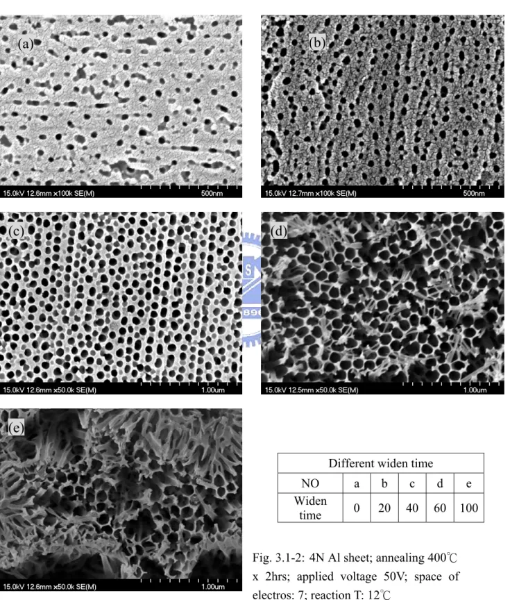
Fig. 3.1-1 depicts the SEM top-view of AAO array morphology formed by 4Ni Al sheet with different annealing temperature. We observed the porous array along a direction in all images and the different phenomenon by the same widening recipe. It appears the intrinsic quality of Al is the major cause, and we suggest the distance is formed by the machine stretch. It can be solved by chemical polish or machine polish.
Fig. 3.1-2 shows the relation of widened time and AAO morphology. We can confirm that the widening time with porous diameter in proportion.
The over widening time was applied; the AAO became brush-liked AAO (Fig. 3.1-3) which was composed by fracture pores on the AAO surface. The structure has been studied34.
Fig. 3.1-4 and Fig. 3.1-5 reveal AAO structures fabricated by multiple step anodization. We observed the more fracture pores on the AAO surface by more step anodization. We observed further the ideal AAO pores array under the fracture pores film in Fig. 3.1-5(a), (c).Fig. 3.1-6 reveals the result of AAO array after supersonic shake procedure. The result equaled to AAO after widening and supersonic shake procedure. We obtained the satisfied AAO array, and the MASK based on the structure.
Fig. 3.1-7 indicates the AAO structures fabricated with the same parameters expect electrolytes. (a) was fabricated by 0.3M oxalic and (b) was fabricated by 0.1M H3PO4 , and both without widening treatment. We
(a) (b)
(e) (f)
(c)
(g) (h)
(a) (b)
(c) (d)
(e)
Fig. 3.1-2: 4N Al sheet; annealing 400 ℃ x 2hrs; applied voltage 50V; space of electros: 7; reaction T: 12℃
Different widen time
NO a b c d e Widen
(a)
(
Fig. 3.1-4: They were fabricated by conventional two-step anodization. (a) SEM image only by fist step anodize (6, 1), (b) Cross section view. (c) SEM image by two-step anodize (6, 1, 3, 1), (d) Cross section view. (4N Al sheet; annealing 400 x 8hrs; applied voltage 40V; space of ℃ electros: 7; reaction T: 28℃)
(a) (b)
Fig. 3.1-5: They were fabricated by multiple step anodization which was more steps then two-step anodize. (a) SEM image by three step anodize (6, 1, 3, 1, 3, 1), (b) Cross section view. (c) SEM image by four step anodize (6, 1, 3, 1, 3, 1, 3, 1), (d) Cross section view. (4N Al sheet; annealing 400 x 8hrs; applied ℃ voltage 40V; space of electros: 7; reaction T: 28℃)
(a) (b)
Fig. 3.1-6: It was cleaned the residuum on the surface by supersonic shock after multiple step anodize. (a) High magnification (100K) SEM image and (b) low magnification (50K) SEM image revealed the uniform pore array. (4N Al sheet; annealing 400 x 8hrs; applied voltage 40V; space of ℃ electros: 7; reaction T: 28℃)
(a)
Fig. 3.1-7: They were fabricated with the same parameters expect electrolytes. SEM images of the same magnification (100K), (a) was fabricated by 0.3M oxalic and (b) was fabricated by 0.1M H3PO4. (4N Al sheet; annealing 400 x ℃
2hrs; applied voltage 40V; space of electros: 7; reaction T: 28℃)
(a)
C
Chhaapp..33..11..22 MMaasskk
Based on the AAO structure, we obtained the MASK by removed the barrier (bottom) layer. The key point was on the recipe of removing bottom and widening.
Fig. 3.1-8 shows the SEM images of MASK, including top-view, back-view, and cross-section view. When removing time was increased, we observed that the thickness of bottom was thinner and the porous wall was thinner simultaneously.
Large area (more than 1cm2) mask would be fabricated by the suitable time combinations with widening and different removing bottom time (Fig. 3.1-9 (c)). Otherwise, we observed partial porous bottom were removed and partial ones were remained (Fig. 3.1-9 (a), (b)), although the (a) and (b) carried out by more reaction time than (a). Based on the isotropic chemical etching, it seems be controlled by the reaction ratio due to contact surface. And the uniformity of the top surface is a problem, it maybe roughness caused of fringe-liked residues of AAO.
Fig. 3.1-8: AAO template (mask) was fabricated by removing bottom layer after removed superfluous Al film with AAO. (a) as-prepared AAO top view of SEM image. (b) The cross section of AAO after removed superfluous Al
(a) (b)
(c) (d)
Fig. 3.1-9: SEM images about back view of AAO with different reaction time combinations which were different widening and different removing bottom time. (a) total time 100 (70+30) mins, (b) 80 (40+40) mins, (c) 60 (0+60)mins. (widening time, removing time)
(
(b) (
Chap. 3.2 ZnO with AAO
Based on the recipe of fabrication AAO on Al sheet, we fabricated on Al/TiN/Si-sub in order to integrate into VLS and increase the applications. Following, the section lists results and discussions including SEM, PL, XRD, TEM, FE measurements.
C
Chhaapp..33..22..11 SSEEMMAAnnaallyyssiiss
Fig. 3.2-1 shows the relation of widened time and AAO morphology. We can confirm that the widening time with porous diameter in proportion according to fabricated once on Al sheet. So we control the widening time to achieve the required aspect ration. However, because of the Al film formed by 4N Al ingot, we observed residues on the surface and effect on porous direction. We suggest the residues formed by impurities precipitated after annealing treatment.
Fig. 3.2-2 reveals the top view of AAO and many residues remain on surface because of the quality Al film was no good enough. And (c) is the high magnification (150K) image indicates porous diameter was about 60-85nm, thickness of porous well was about 50 nm and thickness of bottom was about 50 nm. The thickness of porous well equaled to thickness of bottom. The details of structure was AAO/Al/TiN/Si-sub, the
Fig. 3.2-3Fig. 3.2-3 reveals the bottom layer becomes thinner after over reaction treatment. Relatively, the pores become fracture. We suggest that Si and Ti would tend to from silicide after 400℃annealing, maybe the Al and Ti formed alloy, too. So, we observed a layer existed under the AAO after over suitable second anodic time.
Fig. 3.2-4 reveals clearly the cross-section view of pores full of ZnO successfully, (a): AAO was fabricated by conventional two-step anodization (3, 12) and widened in 60 mins. Diameter of pores was about 80nm, (b): It was removed the ZnO residues on AAO surface after pores full of ZnO by hydrothermal method. Then we removed the AAO by chemical etching in HNO3 solution. It is showed at Fig. 3.2-5 (a) is the top
view of SEM image reveals island-liked ZnO NWs crowd. (b) is the image of cross section view indicates the collapse of ZnO NWs clearly. We observed some broke NWs which stood on the TiN layer vertically, and the other ones which were intact structure were merge together.
Fig. 3.2-6 reveals SEM images of that AAO was fabricated by conventional two-step anodization. The special treatment was supersonic shake to remove residues on surface after widening. We observed the better structure then Fig. 3.2-2, but the porous length was shorter as a result to sacrifice a litter AAO film when the supersonic shake treatment.
As the Fig. 3.2-7, it reveals the different surface morphology of Al film which was evaporated by 4N and 5N Al ingot respectively. We observed lots of impurities on the AAO surface formed by 4N Al source, and another was clean and uniform. Further, the high purity of Al film would provide higher uniform, ordered, vertical pores for applications.
If the reaction temperature of hydrothermal method is too low, we observed those ions could not successfully migrate into pores. Fig. 3.2-8 indicates clearly that the Zno crystallized at top of pores when the reaction temperature was 80 . ℃ The causes maybe include the morphology of AAO and the geometry of pores except the reaction temperature; we suggest the reaction temperature is the principal cause.
Fig. 3.2-9 and Fig. 3.2-10 reveal the morphology of AAO formed by 5N Al film. At
dominate the growth ration of AAO and do not affect the scale of porous diameter.
Fig. 3.2-11 reveals the image which the sample after field emission measurement. (a) is the original structure, diameter: 20-30nm, length: 1800nm. And (b), (c), (d) reveal the broken area after field emission measurement.
Fig. 3.2-1: These AAO were fabricated by two-step anodization (3, 3) on SiO2/Si-sub.
(a), (b) were AAO SEM images without widening treatment, porous of diameter was small then 10nm. (c) (d) were widened in 20 mins, porous of diameter was about 30nm. And (d) (e) were widened in 30 mins, porous of
(a) (b)
(c) (d)
Fig. 3.2-2: AAO was fabricated by conventional two-step anodization (3, 3) and widening time was 40mins. (a) It revealed the top view of AAO and many residues on surface. (b) cross section view image revealed the AAO thickness was about 1.2μ. (c) The high magnification (150K) image indicated porous diameter was about 60-85nm, thickness of porous well was about 50 nm and thickness of bottom was about 50 nm. The thickness of porous well equaled to thickness of bottom. (4N Al /SiO2/Si; thickness of Al:
1μm; annealing 350 x 8hrs; applied voltage: 40V; ℃ electrolyte: 0.3M oxalic; space of electros: 7; reaction T: 12℃)
(a) (b)
(a)
(b)
Fig. 3.2-3: AAO was fabricated by conventional two-step anodization (3, 12). They were anodized over suitable time (about 3min) at second anodic treatment. (a) it was widened in 50 mins. (b) it was widened in 80 mins, we observed over winding induced porous wall to break and thickness of bottom to thinner. (4N Al /TiN/Si; thickness of Al: 1μm; annealing 400 x 8hrs; ℃
(a)
(b)
Fig. 3.2-4: (a) AAO was fabricated by conventional two-step anodization (3, 12) and widened in 60 mins. Diameter of pores was about 80nm. (b) It was removed the ZnO residues on AAO surface after pores full of ZnO by hydrothermal method. The SEM image revealed the pores full of ZnO successfully. (4N Al /TiN/Si; thickness of Al: 1.3μm; annealing 400 x 2hrs; applied voltage: ℃ 40V; electrolyte: 0.3M oxalic; space of electros: 7; reaction T: 12 ; ZnO ℃ hydrothermal in 2hrs at 96℃)
(a)
(b)
Fig. 3.2-5: The AAO full of ZnO was removed AAO in order to form the exposed ZnO NWs. (a). the top view of SEM image revealed island-liked ZnO NWs crowd. (b). the image of cross section view indicated the collapse of ZnO NWs clearly. (4N Al /TiN/Si; thickness of Al: 1.3μm; annealing 400 x ℃ 2hrs; applied voltage: 40V; electrolyte: 0.3M oxalic; space of electros: 7;
(a)
(b) (c)
Fig. 3.2-6: AAO was fabricated by conventional two-step anodization. The special treatment was supersonic shake to remove residues on surface after widening. (a) Top view. (b)Cross-section view and (c) was high magnification (250K) image of the bottom area. (4N Al /TiN/Si; thickness of Al: 1μm; annealing 400 x 8hrs; app℃ lied voltage: 40V; electrolyte: 0.3M oxalic; space of electros: 7; reaction T: 12℃)
(a)
(b)
Fig. 3.2-7: AAO was fabricated by two-step anodization. The top-view SEM images were the same magnification, (a) employed 5N Al source and (b) employed 4N Al source. We could clearly observe the improvement of reduced
(a)
(b) (c)
Fig. 3.2-8: SEM images of cross section(a),top view(b)(c) Temperature not high enough to assist ZnO migrated into pores, so we observed the ZnO covered the surface and would not full into the porous.(b) 30 mins at 80℃,(c) 1hr at 80℃. The inset in (a) was the high magnification SEM image.
(b) (a) (d) (c) (g) (f)
Fig. 3.2-9: SEM images of cross-section view (a)(b)(c) were different applied voltage to anodize according to 30V, 40V, 50V. (d), (e), and (f) were reveled different widening time form the sample of (c), and the widening time was
(a) (b)
(c) (d)
Fig. 3.2-10: (a), (c) are the SEM images of top view, and (b), (d) are SEM images of cross-section view. (a), (b) are fabricated by convectional two-step anodization.(1, 3.5) (c), (d) are widened in 60 mins, the diameter become about 80 nm from 10 nm. (5N Al /TiN/Si; thickness of Al: 500nm; annealing 400 x 2hrs; applied voltage℃ : 50V; electrolyte: 0.3M oxalic; space of electros: 7; reaction T: 12℃)
(b) (a)
(c) (d)
(b)
Fig. 3.2-11: They are SEM images of cross-section view, (a) is the original structure, diameter: 20-30nm, length: 1800nm. And (b), (c), (d) reveal the broken area after field emission measurement. (5N Al /TiN/Si; thickness of Al: 1500nm; annealing 400 x ℃ 2hrs; applied voltage: 50V; electrolyte: 0.3M oxalic; space of electros: 7; reaction T: 12 ; widening time 20℃ )
C
Chhaapp..33..22..22 TTEEMMAAnnaallyyssiiss
About the analysis of TEM, we show data at following. Moreover, we prepared the sample for TEM by FIB (focus ion beam) and supersonic shake method.
Fig. 3.2-12 reveals the high resolution image about the cross-section view of AAO full of ZnO. Fig. 3.2-13 reveals: (a) the TEM image of ZnO NW by supersonic shake treatment; (b) the SAED of ZnO NW. (c) the EDS of ZnO NW.
We observe the SAED pattern which seems the type of crystallization mixes with amorphous and poly. We suggest the crystalline of ZnO maybe a poly type, and the amorphous signal from AAO according to the Al2O3
of AAO is amorphous type. The result is expectable due to the structure of ZnO NW, prepared by supersonic shake treatment, was a ZnO wire covered with a Al2O3 film, the EDS shows the concentration of Zn is
(a)
TEM images
Fig. 3.2-12: The TEM cross-section image of AAO full of ZnO prepared by FIB; ; the porous diameter is about 80nm after 40mins widening treatment; the structure is AAO/SiO2/Si-sub.
(a) (b)
(c)
Fig. 3.2-13: (a) TEM image of ZnO NW prepared by supersonic shake treatment; (b) SAED of ZnO NWs.(c) EDS of ZnO NWs.
C
Chhaapp..33..22..33 XXRRDDAAnnaallyyssiiss
The crystal structure and phase of the NWs were determined by X-ray diffraction (XRD, MAC Science, MXP18, and Japan). Fig. 3.2-14 depicts the XRD patterns of Al thin film under different annealing treatment on TiN/Si-sub, it compares with (a) different annealing time and temperature, (b) RTA, respectively. The major annealing treatment was at 300~500 °C for 1~8 hrs in the Ar atmosphere, and cool down to room temperature in chamber naturally. Another one was rapid thermally annealed (RTA) at 400 or 500 °C for 3 min in the Ar atmosphere. We observe the peak of TiN disappeared due to the higher T and longer time annealing or RTA. It seems to imply that TiN was composed with Al or the quality of TiN deposited by sputter was not good. Actually, we observed interface (between Al film and TiN) adhesion after RTA treatment was inferior to ones after long time annealing. Consequently, we elected some suitable parameter for annealing which annealing was carried out at 400 ℃ for 2hrs, and replaced barrier layer of TiN with SiO2 layer.
At Fig. 3.2-15, those XRD patterns of AAO full of ZnO on SiO2/Si-sub indicate the different crystalline of sample with annealing or
not. The XRD peak at around 33° is caused by the ZnO crystal, and the main peaks indexed as (002) of the wurtzite structure. The batter crystalline of ZnO would exhibit better FE properties according to