AlGaInAs quantum-well 1.3-μm laser by a diode-pumped actively Q-switched
Nd:GdVO
4laser
S. C. Huang , K. W. Su, A. Li, S. C. Liu Y. F. Chen, and K.F. Hunag
Department of Electrophysics, National Chiao Tung University, Hsinchu, Taiwan
We report a high-peak-power AlGaInAs 1.36-µm vertical-external-cavity surface-emitting laser (VECSEL)
optically pumped by a diode-pumped actively Q-switched Nd:GdVO4 1.06-µm laser under room-temperature operation.
The gain medium is an AlGaInAs quantum wells (QWs)/barrier structure grown on a Fe-doped InP substrate by metalorganic chemical-vapor deposition. With an average pump power of 1.9 W, an average output power of 340 mW was obtained at a pulse repetition rate of 40 kHz, corresponding to an optical-to-optical conversion efficiency of 18.76%. With a peak pump power of 7.9 kW, the highest peak output power was 1.3 kW at a pulse repetition rate of 10 kHz.
Keywords: VECSEL ; AlGaInAs ; high-peak power
1.Introduction
High-peak-power all-solid-state laser sources in the 1.3–1.6µm spectral region are of particular interest in
remote sensing, eye-safe optical ranging, fiber sensing, and communication.[1–4] Diode-pumped solid state lasers
(DPSSLs) that have the advantages of relatively compact size, high power, excellent beam quality, long lifetime, and low heat production have been widely used for various applications, including industry, pure science, medical diagnostics, and entertainment.[5] Nevertheless, the spectral range of diode-pumped solid-state laser systems is limited by the properties of existing doped crystals and glasses. Recently, the optically pumped vertical-external cavity surface-emitting semiconductor lasers (VECSELs) conbine the approaches of diode pumped-solid-state lasers and semiconductor quantum-well lasers, drawing on the advantages of both. Besides, by band gap engineering, the gain medium optically pumped VECSEL can be designed to produce laser emission at a chosen wavelength within the
window of growth of the semiconductor material system.[6,7] Typically a VECSEL device consists of a highly
reflecting distributed Bragg reflector (DBR) and a resonant periodic gain structure that comprises a series of barriers to provide the pump absorption, quantum wells (QWs) to provide gain, and layers to prevent oxidation.
The InP-based material could offer a gain region with a smaller lattice mismatch for 1.3µm wavelengths, but the small contrast of refractive indices hinders the performance of the DBRs. As a consequence, until now the InP-based material has never been used as a VECSEL device at 1.3 µm. To reach a wavelength near 1.3 µm, GaInNAs/GaAs QWs
have been developed as a gain medium[8] and a 0.6 W CW output power has been demonstrated.[9] Even so, there has
been no experimental demonstration of room-temperature high-peak-power 1.3 µm laser sources with semiconductor QWs as gain media in an external cavity. In this Letter we report, for the first time to our knowledge, a room-temperature high-peak-power nanosecond semiconductor QW laser at 1.36 µm, using a diode-pumped actively
Q-switched Nd:GdVO4 1.06 µm laser as a pump source.
The gain medium was composed of an AlGaInAs QW/barrier structure grown on an Fe-doped InP transparent substrate. Note that the conventional S-doped InP substrate has significant absorption in the 1.0–2.0 µm spectral region. Since the Fe-doped InP substrate is transparent at the lasing wavelength, the function of the DBRs in the VECSEL
device can be replaced by an external mirror. With an average pump power of 1.8 W, an average output power of 340 mW at a pulse repetition rate of 40 kHz was obtained. The peak output power was up to 1.3 kW at a pulse repetition rate of 10 kHz. Compared with continuous wave pumping/injection, the pulsed pumping scheme can reduce the heat of the
device at room temperature[16] . The present gain medium is an AlGaInAs QW/barrier structure grown on an Fe-doped
InP substrate by metalorganic chemical-vapor deposition. It is worthwhile to mention that the AlGaInAs material
system has a larger conduction band offset than the most widely used InGaAsP system.[10–13] This larger conduction
band offset has been confirmed to yield better electron confinement in the conduction band and higher temperature
stability. The AlGaInAs material has been used as a surface-emitting optical amplifier pumped by a laser diode.[14]
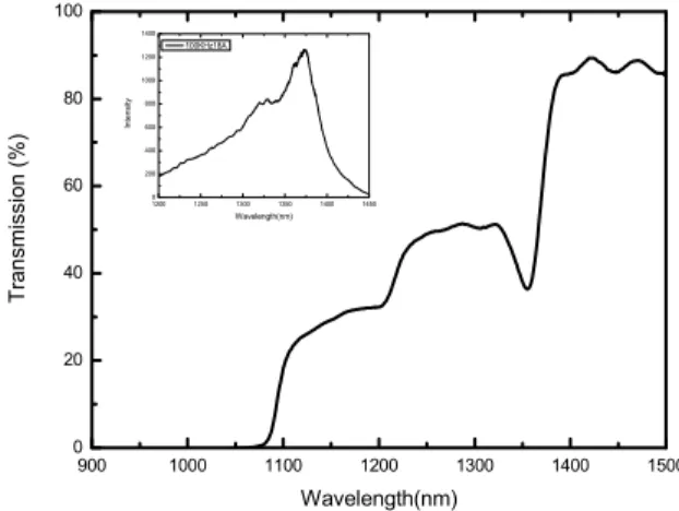
However, until now there has been no experimental realization involving the VECSEL with AlGaInAs. Here the gain region consists of 30 groups of two QWs with the luminescence wavelength around 1365 nm, spaced at half-wavelength intervals by AlGaInAs barrier layers with the bandgap wavelength around 1070 nm. The barrier layers are used not only to absorb the pump light but also to locate the QW groups in the antinodes of the optical field standing wave. An InP window layer was deposited on the gain structure to avoid surface recombination and oxidation. The back side of the substrate was mechanically polished after growth. Both sides of the gain chip were antireflection (AR) coated to reduce back reflections and coupled-cavity effects. The total residual reflectivity of the AR-coated sample is approximately 5%. Figure 1 shows the transmittance spectrum at room temperature for the AR-coated AlGaInAs/InP gain chip. It can be seen that the strong absorption of the barrier layers leads to low transmittance near 1070 nm. The total absorption efficiency of the barrier layers at 1064 nm was found to be approximately 95%. On the other hand, an abrupt change in transmittance near 1365 nm comes from the absorption of the AlGaInAs QWs. The room-temperature spontaneous-emission spectrum, obtained by pulse excitation at 1064 nm, is shown in the inset of Fig. 1. As expected, the emission is quite broad, with a peak around 1365 nm, and has a long tail extending to shorter wavelengths.
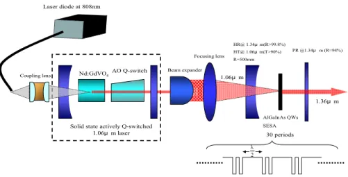
2. Experimental setup
Figure 2 shows the experimental configuration of the room-temperature high-peak-power AlGaInAs QWs
laser at 1365 nm. The pump source is a diode-pumped acousto-optically Q-switched Nd:GdVO4 1064 nm laser to
provide 12-80 ns pulses at repetition rates between 10 and 100 kHz.
900 1000 1100 1200 1300 1400 1500 0 20 40 60 80 100 Tran smi ssi o n (%) Wavelength(nm) 1200 1250 1300 1350 1400 1450 0 200 400 600 800 1000 1200 1400 In tens ity Wavelength(nm) 100KHz18A
Figure 1. The transmittance spectrum at room temperature for AR-coated AlGaInAs/InP gain chip. Inset, room-temperature spontaneous-emission spectrum, obtained by 0.5W pulse excitation at 1064nm
The pump spot diameter is controlled to be 420±20 µm for efficient spatial overlap with the fundamental transverse mode. The gain chip was mounted on a copper heat sink, but no active cooling was applied. The laser resonator is a concave–plano cavity. The input mirror was a 500 mm radius-of-curvature concave mirror with AR coating on the entrance face at 1064 nm(R<0.2%), high-reflection coating at 1365 nm (R>99.8%), and high-transmission coating at 1064 nm on the other surface (T>90%). The reflectivity of the flat output coupler is 94% at 1365 nm. The overall laser cavity length is approximately 10 mm
Coupling lens Nd:GdVO4
Beam expander Focusing lens
Laser diode at 808nm
Solid state actively Q-switched 1.06μ m laser 1.36μ m 1.06μ m AlGaInAs QWs SESA HR@ 1.34μ m(R>99.8%) HT@ 1.06μ m(T>90%) R=500mm PR @1.34μ m (R=94%) 30 periods λ 2 AO Q-switch
Figure 2. Experimental setup of the room-temperature optically pumped AlGaInAs/InP
laser at 1.36μ m
3. Experimental results and discussion
Figure 3 shows the performance of the optically pumped AlGaInAs laser at pump repetition rates of 10, 40,
and 100 kHz. The pump pulse widths for repetition rates of 10, 40, and 100 kHz are approximately 12, 25, and 80 ns, respectively. The cavity decay time is 0.11 ns. The beam quality factor was determined by a Gaussian fit to the laser beam waist, and the divergence angle and was found to be less than 1.5. At a repetition of 10 kHz, the average output power could be up to 134 mW; the output power saturation beyond the average pump power of 1.0 W was due to the thermally induced gain degradation.
0.0 0.3 0.6 0.9 1.2 1.5 1.8 2.1 0 50 100 150 200 250 300 350 Av er age out put pow er @ 1365nm (m W)
Average incident pump power @ 1064nm (W) 10kHz
40kHz 100kHz
Figure 3 : Experimental results for the optically pumped AlGaInAs laser at pump repetition rate of 10, 40 ,100kHz
At a repetition of 10 kHz, due to the pump saturation effects of the barrier layers absorption efficiency of the gain chip for the pump power higher than 0.7 W was found to be significantly reduced. As a consequence, maximum average output power at a repetition rate of 10 kHz was saturated at around 120 mW. With the experimental data on a
was estimated to be 7.7 MW/cm2. This value was 2–3 orders of magnitude higher than conventional solid state laser
crystals because of its shorter fluorescence decay time.[15] However, the lower conversion efficiency at the 100 kHz
repetition rate might be due to the longer pump pulse duration that enhanced the local heating effect.
In other words, management of the thermal effects is necessary to scale up the average output power. Figure 4
shows a typical oscilloscope trace of a train of output and pump pulses and expanded shapes of a single pulses. It can be seen that the output pulses tracked the pump pulses for each pumping case.
50μ s/div 20ns/div Pump (1064 nm) Pump (1064 nm) Output (1365 nm) Output (1365 nm)
Figure. 4. (Color online) (a) Typical oscilloscope trace of a train of pump and output pulses and (b) expanded shapes of a single pulse.
0 1 2 3 4 5 6 7 8 0.0 0.2 0.4 0.6 0.8 1.0 1.2 Pe ak ou tp ut po we r a t 13 65 nm (k W)
Peak incident pump power at 1064nm (kW)
1360 1365 1370 1375 1380 1385 1390 0 2000 4000 6000 8000 10000 12000 14000 Int ens ity (ar b. uni t) Wavelength(nm)
Figure. 5. Experimental results for the peak output power as a function of peak pump power. Inset, typical lasing spectrum obtained with 0.7W of average pump power at a repetition rate of 10 kHz.
Figure 5 shows the peak output power as a function of peak pump power. The peak output power was up to 1.2 kW at a
peak pump power of 7.9 kW, and the slope efficiency was approximately 16%. The typical lasing spectrum shown in the inset of Fig. 5 was obtained with 1.0W of average pump power at a repetition rate of 40 kHz. The lasing spectrum
was composed of dense longitudinal modes, and its bandwidth was up to 20 nm for an average pump power greater than 200 mW. The wide spectral range
indicates the potential for achieving ultra-short pulses in mode-locked operation.
4. Conclusion
In summary, the gain medium is a 30 groups of two AlGaInAs quantum well, spaced at half-wavelength intervals by AlGaInAs barrier layers with the band-gap wavelength around 1070 nm. The gain chip was grown on Fe-doped InP transparent substrate. In a room-temperature high-peak-power nanosecond laser at 1365 nm is obtained. Using an
actively Nd:GdVO4 Q-switched 1064 nm laser to pump the gain chip, an average output power of 340 mW was
obtained at a pulse repetition rate of 40 kHz and an average pump power of 1.9 W corresponding to an optical-to-optical conversion efficiency of 18.76%,. At a pulse repetition rate of 10 kHz, the peak output power was found to be up to 1.2 kW at a peak pump power of 7.9 kW.
Acknowledgement
The authors gratefully acknowledge various AlGaInAs/InP gain chips from True-Light Corporation.
The authors also thank the National Science Council for their financial support of this research under contract NSC-93-2112-M-009-034.
Address correspondence to S.-C. Huang : [email protected]
REFERENCES
[1]. A. S. Grabtchikov, A. N. Kuzmin, V. A. Lisinetskii, V. A. Orlovich, A. A. Demidovich, K. V. Yumashev, N.
V.Kuleshov, H. J. Eichler, and M. V. Danailov,” Passively Q-switched 1.35 µm diode pumped Nd:KGW laser with
V:YAG saturable absorber” Opt.Mater. 16, 349 (2001).
[2]. R. Fluck, R. Häring, R. Paschotta, R. Gini, H. Melchior, and U. Keller,” Eyesafe pulsed microchip laser using semiconductor saturable absorber mirrors” Appl. Phys. Lett. 72, 3273 (1998).
[3]. R. D. Stultz, V. Leyva, and K. Spariosu,” Short pulse, high-repetition rate, passively Q-switched
Er:yttrium-aluminum-garnet laser at 1.6 microns” Appl. Phys. Lett. 87, 241118 (2005).
[4]. V. G. Savitski, N. N. Posnov, P. V. Prokoshin, A. M. Malyarevich, K. V. Yumashev, M. I. Demchuk, and A.A.
Lipovski,” PbS-doped phosphate glasses saturable absorbers for 1.3-µm neodymium lasers” Appl. Phys. B 75, 841
(2002).
[5]. D. L. Spies,” Highly efficient neodymium:yttrium aluminum garnet laser end pumped by a semiconductor laser
array” Appl. Phys. Lett. 47, 74 (1985).
[6]. M. Kuznetsov, F. Hakimi, R. Sprague, and A. Mooradian,” Design and characteristics of high-power(>0.5-W)diode-pumped vertical-external-cavity surface-emitting semiconductorlasers with circular
TEM00 beams” IEEE J. Sel. Topics Quantum Electron. 5, 561 (1999).
[7]. A. C. Tropper, H. D. Foreman, A. Garnache, K. G. Wilcox, and S. H. Hoogland, “Vertical-external-cavity semiconductor lasers” J. Phys. D 39, R74 (2004).
[8]. M. Kondow, K. Uomi, A. Niwa, T. Kitatani, S.Watahiki, and Y. Yazawa,” GaInNAs: a novel material for
long-wavelength-range laser diodes with excellent high-temperature performance” Jpn. J. Appl. Phys. Part 1
[9]. J. M. Hopkins, S. A. Smith, C. W. Jeon, H. D. Sun, D. Burns, S. Calvez, M. D. Dawson, T. Jouhti, and M. Pessa,” 0.6 W CW GaInNAs vertical external-cavity surface emitting laser operating at 1.32 /spl mu/m”Electron. Lett. 4, 30 (2004).
[10]. C. E. Zah, R. Bhat, B. N. Pathak, F. Favire, W. Lin, M. C. Wang, N. C. Andreadakis, D. M. Hwang, M. A. Koza, T. P. Lee, Z. Wang, D. Darby, D. Flanders, and J. J.Hsieh,” High-performance uncooled 1.3-µm AlxGayIn1-x-yAs/InP strained-layer quantum-well lasers for subscriberloop applications” IEEE J. Quantum Electron. 30, 511 (1994).
[11]. J. Minch, S. H. Park, T. Keating, and S. L. Chuang,” Theory and experiment of In1-xGaxAsyP1-y and
In1-x-yGaxAlyAs long-wavelength strained quantum-well lasers” IEEE J. Quantum Electron. 35, 771 (1999).
[12]. S. R. Selmic, T. M. Chou, J. P. Sih, J. B. Kirk, A. Mantie, J. K. Butler, D. Bour, and G. A. Evans,” Design and characterization of 1.3-µm AlGaInAs-InPmultiple-quantum-well lasers”IEEE J. Sel. Top. Quantum Electron. 7, 340 (2001).
[13]. N. Nishiyama, C. Caneau, B. Hall, G. Guryanov, M. H. Hu, X. S. Liu, M.-J. Li, R. Bhat, and C. E. Zah,”Long-wavelength vertical-cavity surface-emitting lasers on InP with lattice matched AlGaInAs-InP DBR grown by MOCVD” IEEE J.Sel. Top. Quantum Electron. 11, 990 (2005).
[14]. O. Hanaizumi, K. T. Jeong, S. Y. Kashiwada, I. Syuaib, K. Kawase, and S. Kawakami, “Observation of gain in an optically pumped surface-normal multiple-quantum-well optical amplifier”Opt. Lett. 21, 269 (1996).
[15]. F. Sanchez, M. Brunel, and K. Aït-Ameur,”Pump-saturation effects in end-pumped solid-state lasers” J. Opt. Soc.
Am. B 15, 2390 (1998).
[16]. N. Hempler, J.M Hopkins, A.J Kemp “Pulse pumping of semiconductor disk lasers” Opts express No.6 , Vol.15 2007