10 IEEE TRANSACTIONS ON DEVICE AND MATERIALS RELIABILITY, VOL. 12, NO. 1, MARCH 2012
Diode-Triggered Silicon-Controlled Rectifier
With Reduced Voltage Overshoot
for CDM ESD Protection
Wen-Yi Chen, Student Member, IEEE, Elyse Rosenbaum, Fellow, IEEE, and Ming-Dou Ker, Fellow, IEEE
Abstract—Diode-triggered silicon-controlled rectifiers (DTSCRs)
are used for on-chip electrostatic discharge protection. The role
of the trigger diode string in determining the transient voltage
overshoot is investigated using a very fast transmission line pulse.
A DTSCR containing only poly-bound trigger diodes has a voltage
overshoot of just 1.5 V at 7 A, which is significantly less than what
is found with STI-bound diodes. A DTSCR with only STI-bound
trigger diodes has a lower leakage current. Therefore, DTSCRs
with different trigger diode configurations may be suitable for
different applications, e.g., high speed or low power.
Index Terms—Charge device model (CDM), electrostatic
discharge (ESD), silicon-controlled rectifier (SCR).
I. I
NTRODUCTIONS
ILICON-CONTROLLED RECTIFIER (SCR) devices
safely handle high current densities, making them
attrac-tive for electrostatic discharge (ESD) protection [1]. Various
designs have been proposed to further improve the ESD
protec-tion efficiency of SCR. For example, the structure in [2] utilizes
a dummy-gate structure to improve the turn-on speed of the
SCR device. Among the various SCR-based ESD protection
de-signs, the diode-triggered SCR (DTSCR) prevails in advanced
CMOS technologies due to its design simplicity [3], [4]. When
SCR-based protection devices are subject to nanosecond-scale
discharges, such as charged device model (CDM) ESD, they
are often unable to clamp the pad voltage below the breakdown
voltage of thin gate oxides, particularly in sub-100-nm CMOS
technologies [5]–[10]. Although the holding voltage of a typical
SCR is about 1.5 V, the device cannot be switched instantly
from off to on; if the applied ESD pulse has a subnanosecond
Manuscript received July 19, 2011; revised September 7, 2011 and September 26, 2011; accepted October 1, 2011. Date of publication October 13, 2011; date of current version March 7, 2012. This work was supported in part by the National Science Council, Taiwan, under Contract NSC 98-2221-E-009-113-MY2 and in part by the “Aim for the Top University Plan” of National Chiao Tung University and the Ministry of Education, Taiwan. The work of W.-Y. Chen was supported by the Graduate Students Study Abroad Fellowship from the National Science Council, Taiwan. The work of E. Rosenbaum was supported by the SRC.W.-Y. Chen is with the Institute of Electronics, National Chiao Tung Univer-sity, Hsinchu 300, Taiwan.
E. Rosenbaum is with the Department of Electrical and Computer Engineer-ing, University of Illinois at Urbana–Champaign, Urbana, IL 61801 USA.
M.-D. Ker is with the Department of Electronics Engineering, National Chiao Tung University, Hsinchu 300, Taiwan, and also with the Department of Electronic Engineering, I-Shou University, Kaohsiung 840, Taiwan (e-mail: [email protected]).
Color versions of one or more of the figures in this paper are available online at http://ieeexplore.ieee.org.
Digital Object Identifier 10.1109/TDMR.2011.2171487
TABLE I
TESTSTRUCTURESSTUDIED INTHISWORK
rise time, a transient voltage overshoot is observed [11], and it
requires that the SCR be augmented by an additional protection
element [12], [13]. Before the SCR fully turns on, the voltage
across its terminals is determined by the trigger circuit [14].
This observation suggests that one should employ a trigger
circuit that turns on quickly to provide good voltage clamping.
At high frequencies, diodes exhibit inductive characteristics
as a result of conductivity modulation [15]. This indicates that
the diode string trigger circuit of a DTSCR will itself display
some transient voltage overshoot [14]. In a given technology
node, poly-bound diodes [16] have smaller voltage overshoot
than do STI-bound diodes, a result of the shorter base region
[17]. It follows that a DTSCR built using poly-bound diodes
should provide better voltage clamping than would one built
using STI-bound diodes. This work evaluates that conjecture by
means of experiments performed on DTSCR devices fabricated
in a 65-nm low-power CMOS technology.
II. E
XPERIMENTThe test structures used in this work are listed in Table I. The
DTSCRs all contain three external p
+/n-well diodes, labeled
as D
2, D
3, and D
4in Fig. 1(a). D
2, D
3, and D
4each have a p-n
junction perimeter of 200 μm. In test structure A (STI-DTSCR),
these are STI-bound diodes with a p
+-to-n
+spacing of 360 nm.
Test structure B (Diode-String) is similar to A, except that the
n
+cathode of the SCR has been removed, disabling the SCR
and allowing one to observe the characteristics of just the diode
string. In test structure C (Mix-DTSCR), D2, D3, and D4
are
poly-bound diodes with a p
+-to-n
+spacing (gate width) of
65 nm. Test structure D (Poly-DTSCR) is similar to C, except
that D1, the trigger diode integrated within the SCR, has been
changed from STI-bound to poly-bound. The cross section of a
Poly-DTSCR is shown in Fig. 1(b).
In all cases, the SCR has an effective width of 50 μm;
this also means that D1
has a 50-μm perimeter. The SCR
1530-4388/$26.00 © 2011 IEEEFig. 1. (a) Schematic representation of the DTSCRs used in this work and (b) cross section of a Poly-DTSCR.
anode-to-cathode spacing (Sac) was fixed at the minimum
value allowed by the layout design rules, which is 0.36 μm,
so as to minimize the intrinsic turn-on delay of the SCR [4].
A very-fast transmission line pulse (vf-TLP) system is used
to generate pulses with a pulse width of 5 ns and a rise time of
100 ps [18], [19]. These pulses are applied to the DTSCRs, and
the device response is recorded using a 12-GHz oscilloscope.
III. VF-TLP R
ESULTS ANDD
ISCUSSIONA single quasi-static I–V point is obtained from the vf-TLP
data by averaging the current and voltage over a 500-ps interval,
starting 3 ns after the pulse rising edge (see Fig. 3). The
result-ing I–V curves are shown in Fig. 2(a). There are three regions
in the quasi-static I–V curve: (I) SCR is off, and VDUT
< V
t1,
where V
t1is the on-voltage of the diode string; (II) SCR is on;
and (III) SCR is on, and the diode string is also on, because
V
DUT> V
t1. In regions I and II, the three DTSCRs have
nearly identical quasi-static I–V characteristics. In region III,
where the SCR and the diode string provide parallel paths for
the ESD current, the Poly-DTSCR has lower on-resistance than
the other two DTSCRs because the poly-bound diodes have a
smaller static Ron
than the STI-bound diodes.
In Fig. 2(b), the current is instead plotted as a function of
the peak voltage appearing across the device under test (DUT).
The STI-DTSCR and the Diode-String have nearly identical
I–V characteristics, at least for V
peak< 13 V, highlighting
that Vpeak
is determined by the trigger circuit, not the SCR.
Changing the SCR-based structure from STI-DTSCR to
Poly-DTSCR dramatically reduces the amount of voltage overshoot
(V
OV), not only because the poly-bound diodes have a lower
static R
onthan STI-bound diodes but also because they display
less inductive behavior.
Fig. 2. (a) Quasi-static I–V characteristics and (b) peak overshoot voltage versus quasi-static current for the different test structures. Data extracted from vf-TLP.
Two additional observations are made in regard to the data
in Fig. 2(b). First, the Mix-DTSCR provides only marginally
better voltage clamping than does the STI-DTSCR. Defining
V
OV= Vpeak
− V
DUT, the Mix-DTSCR provides only abouta 2-V reduction in VOV
at 7 A. This result indicates that, in
the Mix-DTSCR, the STI-bound diode D1
dominates the total
impedance of the current path from D1
to D4, at least on the
subnanosecond time scale.
Second, the I–V curve for the Mix-DTSCR shows a gradual
slope change starting at around 12 V, which is the n-well/
p-well junction breakdown voltage; this is attributed to
avalanche-generated electrons flooding the n-well of D
1and
reducing its on-resistance. This effect is not seen in the I–V
curves of the STI-DTSCR and the Diode-String because their
on-resistances are dominated by the STI-bound diodes D
2, D
3,
and D4; in contrast, the I–V curves for these devices undergo
a sudden slope change at about 13.5 V. This has been attributed
to n-well/p-well junction breakdown followed by the triggering
of the parasitic SCR between the p
+of D1
and the n
+of D4,
which provides an additional current path in parallel with the
trigger circuit [14]; the parasitic SCR is triggered at a
volt-age higher than the 12-V junction breakdown voltvolt-age because
each diode in the DTSCR is surrounded by a p
+guard ring
[see Fig. 1(b)] [20]. The Diode-String’s quasi-static I–V curve
[Fig. 2(a)] similarly undergoes a slope change at 13.5 V.
In Fig. 3, V
DUT(t) for all three DTSCRs is plotted for
pulses with I
DUT= 2 A. The voltage across the Poly-DTSCR
12 IEEE TRANSACTIONS ON DEVICE AND MATERIALS RELIABILITY, VOL. 12, NO. 1, MARCH 2012
Fig. 3. VF-TLP. Measured voltage waveforms for different DTSCRs.
Fig. 4. Simulated transient waveforms for STI-DTSCR and Poly-DTSCR.
is clamped to 6 V, whereas it nearly reaches 10 V in the
Mix-DTSCR and exceeds 11 V in the STI-DTSCR. However,
the Poly-DTSCR reaches its steady-state voltage more slowly,
with VDUT(t) showing a shoulder rather than collapsing rapidly
toward its final value. In fact, between 0.5 and 0.9 ns, the
voltage across the Poly-DTSCR is higher than that across the
STI-DTSCR or the Mix-DTSCR. To understand this result,
the transient responses of STI-DTSCR and Poly-DTSCR were
simulated using Cadence Virtuoso Spectre. The trigger diodes
are modeled using the same approach presented in [21]. The
SCRs are modeled as cross-coupled n-p-n and p-n-p transistors;
model parameters are provided by the foundry based on the
Gummel–Poon BJT model. The simulation results are shown in
Fig. 4; the simulated V
DUT(t) looks quite similar to V
DUT(t)
obtained from vf-TLP measurement. The simulated current
in D4
(i.e., through the diode string), I
D, is also plotted in
Fig. 4. I
Dfor the STI-DTSCR has a slower rise time than
that for the Poly-DTSCR, and I
Dcontinues to flow at later
time points in the STI-DTSCR. I
Daugments current flow
through the SCR, thereby helping to reduce the voltage at the
anode; a faster turnoff of I
Dremoves the supplemental current
path. In the Poly-DTSCR, once the diode string turns off, the
decay of the anode voltage is determined solely by the intrinsic
SCR and is a relatively slow process. Despite the shoulder
in its VDUT
(t), the Poly-DTSCR is still the best CDM ESD
protection device among the investigated DTSCRs due to its
substantially reduced peak voltage.
Fig. 5. Quasi-static I–V characteristics of different DTSCRs, extracted from 100-ns TLP.
TABLE II
MEASUREMENTRESULTS OFDIFFERENTDTSCRS
IV. A
DDITIONALP
ERFORMANCEM
ETRICSQuasi-static I–V characteristics obtained from 100-ns TLP
[22] measurements are shown in Fig. 5. Because all DTSCRs
have the same anode-to-cathode spacing, all three DTSCRs
have the same holding voltage of 1.5 V. The trigger voltage
and current V
t1and I
t1are obtained from the data shown in
the figure inset. The failure current (Ifail) is defined as the TLP
current which causes the leakage (measured at 1 V) to increase
by more than 10%. The test structure layout did not permit
for measurement of the device S-parameters, which would
allow for accurate measurement of the capacitance with the
bondpads and other parasitics de-embedded. However, using an
LCR meter to measure the total capacitance of each structure,
one can easily observe the incremental increase in capacitance
as the trigger diodes are changed from STI-bound to
poly-bound. The values of V
OV, V
t1, I
t1, I
fail, and C are listed in
Table II. The Poly-DTSCR has slightly reduced I
fail, slightly
increased capacitance, and greatly increased leakage (5
×)
rela-tive to the STI-DTSCR.
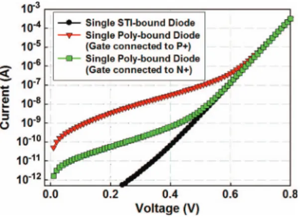
The dc I–V characteristics of stand-alone diodes are shown
in Fig. 6. Below 0.6 V, the gate leakage current dominates the
junction leakage current, and the poly-bound diode conducts
more current than the STI-bound diode. The large leakage
current of poly-bound diodes explains why the Poly-DTSCR
has higher leakage current than the STI-DTSCR. The
poly-bound diodes used in this work each have their gate tied to
their anode, i.e., the p
+side. The measurement results in
Fig. 6 suggest that the leakage current of a Poly-DTSCR can
likely be reduced below the value shown in Table II simply by
changing the gate connection from the anode to the cathode
Fig. 6. DC I–V characteristics of a single STI-bound diode and a single poly-bound diode with varying gate connections. Both diodes have the same p-n junction perimeter of 200 μm.
(p
+to n
+). Measurement results indicate that such a change
also reduces the capacitance of the diode and does not affect
its ESD performance, results confirmed by the data in [23]
and [24].
V. C
ONCLUSIONThe trigger circuit used with an SCR-based ESD protection
device determines the magnitude of the voltage overshoot that
occurs before the SCR fully turns on. Poly-bound diodes exhibit
reduced voltage overshoot relative to STI-bound diodes; this
work demonstrates that, when poly-bound diodes are integrated
into a DTSCR, the resulting structure provides very good
voltage clamping (an experimental finding recently confirmed
by others [25]). All the diodes in the trigger circuit, including
the diode intrinsic to the SCR, must be poly-bound to obtain the
benefit.
Depending on whether low power or high speed is the design
objective, either an STI-DTSCR or a Poly-DTSCR may be
the better selection. The STI-DTSCR has significantly lower
leakage current and can be augmented by a secondary
protec-tion circuit in order to provide CDM ESD protecprotec-tion.
How-ever, the secondary protection will reduce the performance of
radio-frequency or high-speed input/output circuits. The
Poly-DTSCR reduces the need for a secondary protection at the cost
of increased leakage current.
A
CKNOWLEDGMENTTest structures were fabricated under the TSMC University
Shuttle Program.
R
EFERENCES[1] M.-D. Ker and K.-C. Hsu, “Overview of on-chip electrostatic discharge protection design with SCR-based devices in CMOS integrated cir-cuits,” IEEE Trans. Device Mater. Rel., vol. 5, no. 2, pp. 235–249, Jun. 2005.
[2] M.-D. Ker and K.-C. Hsu, “SCR device fabricated with dummy-gate structure to improve turn-on speed for effective ESD protection in CMOS technology,” IEEE Trans. Semicond. Manuf., vol. 18, no. 2, pp. 320–327, May 2005.
[3] M. Mergens, C. Russ, K. Verhaege, J. Armer, P. Jozwiak, R. Mohn, B. Keppens, and C. Trinh, “Speed optimized diode-triggered SCR
(DTSCR) for RF ESD protection of ultra-sensitive IC nodes in advanced technologies,” IEEE Trans. Device Mater. Rel., vol. 5, no. 3, pp. 532–542, Sep. 2005.
[4] J. Di Sarro, K. Chatty, R. Gauthier, and E. Rosenbaum, “Study of design factors affecting turn-on time of silicon controlled rectifiers (SCRs) in 90 and 65 nm bulk CMOS technologies,” in Proc. IEEE Int. Rel. Phys. Symp., 2006, pp. 163–168.
[5] T. Smedes and N. Guitard, “Harmful voltage overshoots due to turn-on behaviour of ESD protections during fast transients,” in Proc. EOS/ESD
Symp., 2007, pp. 357–365.
[6] C. Chu, A. Gallerano, J. Watt, T. Hoang, T. Tran, D. Chan, W. Wong, J. Barth, and M. Johnson, “Using VFTLP data to design for CDM robust-ness,” in Proc. EOS/ESD Symp., 2009, pp. 286–291.
[7] N. Jack and E. Rosenbaum, “ESD protection for high-speed receiver circuits,” in Proc. IEEE Int. Rel. Phys. Symp., 2010, pp. 835–840. [8] J. Wu, P. Juliano, and E. Rosenbaum, “Breakdown and latent damage of
ultra-thin gate oxides under ESD stress conditions,” in Proc. EOS/ESD
Symp., 2000, pp. 287–295.
[9] A. Ille, W. Stadler, A. Kerber, T. Pompl, T. Brodbeck, K. Esmark, and A. Bravaix, “Ultra-thin gate oxide reliability in the ESD time domain,” in
Proc. EOS/ESD Symp., 2006, pp. 285–294.
[10] D. Ellis, Y. Zhou, J. Salcedo, J.-J. Hajjar, and J. Liou, “Prediction and modeling of thin gate oxide breakdown subject to arbitrary transient stresses,” IEEE Trans. Electron Devices, vol. 57, no. 9, pp. 2296–2305, Sep. 2010.
[11] G. Wybo, S. Verleye, B. Van Camp, and O. Marichal, “Characterizing the transient device behavior of SCRs by means of VFTLP waveform analysis,” in Proc. EOS/ESD Symp., 2007, pp. 366–375.
[12] J. Bourgeat, C. Entringer, P. Galy, P. Fonteneau, and M. Bafleur, “Local ESD protection structure based on silicon controlled rectifier achieving very low overshoot voltage,” in Proc. EOS/ESD Symp., 2009, pp. 314–321.
[13] K. Watanabe, T. Hiraoka, T. Sei, and K. Numata, “New protection tech-niques and test chip design for achieving high CDM robustness,” in Proc.
EOS/ESD Symp., 2008, pp. 332–338.
[14] R. Gauthier, M. Abou-Khalil, K. Chatty, S. Mitra, and J. Li, “Investiga-tion of voltage overshoots in diode triggered silicon controlled rectifiers (DTSCRs) under very fast transmission line pulsing (VFTLP),” in Proc.
EOS/ESD Symp., 2009, pp. 334–343.
[15] I. Ladany, “An analysis of inertial inductance in a junction diode,” IRE Trans. Electron Devices, vol. 7, no. 4, pp. 303–310, Oct. 1960.
[16] M.-D. Ker, K.-H. Lin, and C.-H. Chuang, “MOS-bounded diodes for on-chip ESD protection in a 0.15-μm shallow-trench-isolation salicided CMOS process,” in Proc. IEEE Int. Symp. VLSI Technol. Syst. Appl., 2003, pp. 84–87.
[17] J.-R. Manouvrier, P. Fonteneau, C.-A. Legrand, P. Nouet, and F. Azais, “Characterization of the transient behavior of gated/STI diodes and their associated BJT in the CDM time domain,” in Proc. EOS/ESD Symp., 2007, pp. 165–174.
[18] E. Grund and R. Gauthier, “VF-TLP systems using TDT and TDRT for Kelvin wafer measurements and package level testing,” in Proc. EOS/ESD
Symp., 2004, pp. 338–345.
[19] S. Malobabic, J. Salcedo, J.-J. Hajjar, and J. Liou, “Analysis of safe operating area of NLDMOS and PLDMOS transistors subject to transient stresses,” IEEE Trans. Electron Devices, vol. 57, no. 10, pp. 2655–2663, Oct. 2010.
[20] U. Glaser, K. Esmark, M. Streibl, C. Russ, K. Domanski, M. Ciappa, and W. Fichtner, “SCR operation mode of diode strings for ESD protection,” in Proc. EOS/ESD Symp., 2005, pp. 60–69.
[21] M. Stockinger, S. Ruth, J. Miller, K. Nguyen, Y. Akrout, M. Kearney, B. Drew, and S. Ngo, “CDM protection design for CMOS applications using RC-triggered rail clamps,” in Proc. EOS/ESD
Symp., 2009, pp. 91–100.
[22] A. Gerdemann, K. Bhatia, and E. Rosenbaum, “A Kelvin transmission line pulsing system with optimized oscilloscope ranging,” in Proc. EOS/ESD
Symp., 2007, pp. 80–88.
[23] S. Cao, A. Salman, J.-H. Chun, S. Beebe, M. Pelella, and R. Dutton, “Design and characterization of ESD protection devices for high-speed I/O in advanced SOI technology,” IEEE Trans. Electron Devices, vol. 57, no. 3, pp. 644–653, Mar. 2010.
[24] S. Voldman, S. Geissler, J. Nakos, J. Pekarik, and R. Gauthier, “Semi-conductor process and structural optimization of shallow trench isolation-defined and polysilicon-bound source/drain diodes for ESD networks,” in
Proc. EOS/ESD Symp., 1998, pp. 151–160.
[25] J. Li, R. Gauthier, J. Di Sarro, and R. Mishra, presented at the Int. Electrostatic Discharge Workshop, 2011.
14 IEEE TRANSACTIONS ON DEVICE AND MATERIALS RELIABILITY, VOL. 12, NO. 1, MARCH 2012
Wen-Yi Chen (S’03) received the B.S. degree from
the Department of Electronics Engineering, National Chiao Tung University, Hsinchu, Taiwan, in 2003 and the M.S. degree from the Institute of Electronics, National Chiao Tung University, in 2005, where he is currently working toward the Ph.D. degree.
After military service, he joined the Circuit De-sign Department, SoC Technology Center, Industrial Technology Research Institute, Hsinchu, as a Circuit Design Engineer. In 2006, he joined the Amazing Microelectronic Corporation, where he worked with system-level electrostatic discharge (ESD) protection design. His current re-search interests include reliability of high-voltage CMOS devices and ESD protection design in mixed-voltage I/O circuits.
Elyse Rosenbaum (F’11) received the B.S.
de-gree (with distinction) in electrical engineering from Cornell University, Ithaca, NY, in 1984, the M.S. degree in electrical engineering from Stanford Uni-versity, Stanford, CA, in 1985, and the Ph.D. de-gree in electrical engineering from the University of California, Berkeley, in 1992.
From 1984 to 1987, she was a Member of Techni-cal Staff with AT&T Bell Laboratories, Holmdel, NJ. She is currently a Professor with the Department of Electrical and Computer Engineering, University of Illinois, Urbana. She has been a Visiting Professor with Katholieke Universiteit, Leuven, Belgium, and National Chiao Tung University, Hsinchu, Taiwan. She has authored or coauthored over 100 technical papers. She has given invited lectures at many universities and industrial laboratories. Her present research interests include design, testing, modeling, and simulation of electrostatic dis-charge (ESD) protection circuits, ESD reliability of stacked packaging, design of high-speed circuits with ESD protection, latch-up, gate oxide degradation, and substrate noise coupling.
Dr. Rosenbaum was a recipient of a Best Student Paper Award from the IEDM, a Technical Excellence Award from the SRC, a NSF CAREER Award, a IBM Faculty Award, and a UIUC Bliss Faculty Scholar Award. She is an Editor for IEEE TRANSACTIONS ONDEVICE ANDMATERIALSRELIABILITY. She has presented tutorials on reliability physics at the International Reliability Physics Symposium, the EOS/ESD Symposium, and the RFIC Symposium. She was the Keynote Lecturer at the 2004 Taiwan ESD Conference.
Ming-Dou Ker (S’92–M’94–SM’97–F’08) received
the Ph.D. degree from the Institute of Electronics, National Chiao Tung University, Hsinchu, Taiwan, in 1993.
He was the Department Manager with the VLSI Design Division, Computer and Communication Re-search Laboratories, Industrial Technology ReRe-search Institute, Hsinchu. Since 2004, he has been a Full Professor with the Department of Electronics En-gineering, National Chiao Tung University. During 2008–2011, he was rotated to be the Chair Professor and the Vice President of I-Shou University, Kaohsiung, Taiwan. He is currently a Distinguished Professor with the Department of Electronics Engineering, National Chiao Tung University. During 2010–2011, he was the Executive Director of the National Science and Technology Program on System-on-Chip, Taiwan. He is currently the Executive Director of the National Science and Technology Program on Nano Technology, Taiwan (2011–2014). In the technical field of reliability and quality design for microelectronic circuits and systems, he has published over 400 technical papers in international journals and conferences. He has proposed many solutions to improve the reliability and quality of integrated circuits, which have been granted with 187 U.S. patents and 162 Taiwan patents. He had been invited to teach and/or to consult the reliability and quality design for integrated circuits by hundreds of design houses and semiconductor companies in the worldwide IC industry. His current research interests include reliability and quality design for nanoelectronics and gigascale systems, high-speed and mixed-voltage I/O interface circuits, on-glass circuits for system-on-panel applications, and biomimetic circuits and systems for intelligent prosthesis.
Dr. Ker has served as a member of the Technical Program Committee and the Session Chair of numerous international conferences for many years. He served as the Associate Editor for the IEEE TRANSACTIONS ONVLSI SYSTEMS
in 2006–2007. He was selected as the Distinguished Lecturer in the IEEE Circuits and Systems Society (2006–2007) and in the IEEE Electron Devices Society (2008–present). He was the President of Foundation in Taiwan ESD Association. In 2009, he was awarded as one of the top ten distinguished inventors in Taiwan.