This content has been downloaded from IOPscience. Please scroll down to see the full text.
Download details:
IP Address: 140.113.38.11
This content was downloaded on 21/07/2015 at 09:32
Please note that terms and conditions apply.
Bipolar tri-state resistive switching characteristics in Ti/CeOx/Pt memory device
View the table of contents for this issue, or go to the journal homepage for more 2014 Chinese Phys. B 23 126101
Bipolar tri-state resistive switching characteristics in Ti/CeO
x
/Pt
memory device
M. Ismaila)b)†, M. W. Abbasa), A. M. Ranaa), I. Taliba), E. Ahmeda), M. Y. Nadeema), T. L. Tsaib), U. Chandb), N. A. Shahc), M. Hussaind), A. Aziza), and M. T. Bhattia)
a)Department of Physics, Bahauddin Zakariya University, Multan-60800, Pakistan
b)Department of Electronics Engineering and Institute of Electronics, National Chiao Tung University, Hsinchu 30010, Taiwan, China
c)Thin Films Technology Research Laboratory, Department of Physics, COMSATS Institute of Information Technology, Islamabad-45320, Pakistan
d)Center for High Energy Physics, University of Punjab, Lahore-54590, Pakistan
(Received 21 May 2014; revised manuscript received 4 July 2014; published online 10 October 2014)
Highly repeatable multilevel bipolar resistive switching in Ti/CeOx/Pt nonvolatile memory device has been
demon-strated. X-ray diffraction studies of CeO2 films reveal the formation of weak polycrystalline structure. The observed
good memory performance, including stable cycling endurance and long data retention times (> 104s) with an acceptable resistance ratio (∼102), enables the device for its applications in future non-volatile resistive random access memories
(RRAMs). Based on the unique distribution characteristics of oxygen vacancies in CeOxfilms, the possible mechanism of
multilevel resistive switching in CeOxRRAM devices has been discussed. The conduction mechanism in low resistance
state is found to be Ohmic due to conductive filamentary paths, while that in the high resistance state was identified as Ohmic for low applied voltages and a space-charge-limited conduction dominated by Schottky emission at high applied voltages.
Keywords: multilevel resistive switching, Schottky emission, cerium oxide, oxygen vacancy PACS: 61.05.cp, 73.40.Rw, 73.50.−h, 77.22.Jp DOI:10.1088/1674-1056/23/12/126101
1. Introduction
Nonvolatile memory for multilevel storage has been ex-tensively exploited in portable electronic products.[1–4] How-ever, traditional nonvolatile floating gate memory devices have confronted some physical limits as they are contin-uously scaled down.[5–7] Resistive random access memory (RRAM) is being considered as one of the potential candi-dates for development of the next generation nonvolatile mem-ory because of its advantages such as low energy consump-tion, high density, simple device structure, and intrinsic fast switching speed.[8–10]RRAM devices are based on conductor– dielectric–conductor sandwich structures which can reversibly be switched between two distinct resistance states by apply-ing appropriate voltage.[11,12]In contrast to the conventional memory switching between the two resistance states (HRS and LRS), another kind of switching is also possible where device resistance switches between three or more levels, known as multilevel resistive switching (RS). Multilevel RS enhances storage capability which eventually leads to higher packing density of memory.[13] Many researchers have studied mul-tilevel set/reset and tri-state RRAM devices based on rare earth/transition metal oxides.[14–17]Multilevel resistive states are usually achieved either by controlling the current compli-ance during the SET process or by limiting the amplitude of the voltage pulse during the RESET process. However, in our device (present study), tri-level resistance states were achieved via controlling the set and reset voltages. That is why physical
origin of multilevel resistive switching is different in dissim-ilar devices. The multilevel bipolar switching in Cu/TaOx/Pt
device has been reported by Yang et al.[17] which was sug-gested due to the coupling effect between existing resistive switching mechanisms. On the other hand, a research group at Peking University has explained the multilevel bipolar re-sistance switching mechanism in Al/CeOx/Pt device[15,16]in
terms of formation and rupture of conducting filaments com-posed of oxygen vacancies. Therefore, a deep understanding of characteristics and mechanism of multilevel set/reset resis-tive switching in oxide-based memory structures is still a chal-lenge to be addressed for potential nonvolatile RRAM appli-cations.
In this study, multilevel bipolar RS characteristics in the nonstoichiometric CeOx-based RRAM device with different
top electrode as reported earlier[15,16]are being demonstrated.
Bipolar resistive switching behavior in our Ti/CeOx/Pt
mem-ory device retains stable resistance ratio of approximately ∼102with switching response for more than 3 × 10²cycles.
It is expected that the top electrode reacts with the CeO2layer
and forms an interfacial TiOxlayer. This oxygen-rich top
in-terface area might play a key role in the formation and rupture of conductive filaments during multilevel resistive switching.
2. Experimental procedure
In this work, Ti/CeO2/Pt-based MIM sandwich structures
were fabricated. Ceria (CeO2) films of 30 nm were deposited
†Corresponding author. E-mail:[email protected]
on Pt/Ti/SiO2/Si substrates at room temperature using radio
frequency (rf) magnetron sputtering of a ceramic CeO2
tar-get. Ceria film was prepared at a fixed rf power of 100 W and with argon:oxygen (6:12) flow rate of 20 sccm. The working pressure during deposition was kept at 10 mTorr (1 Torr = 1.33322 × 10² Pa). To complete the metal–insulator–metal structure, a 50-nm thick Ti top electrode was deposited by electron beam evaporation at ambient temperature with a di-ameter of 150 µm patterned through a metallic shadow mask. Pt film (20 nm) was used to avoid the oxidation of Ti elec-trode and to prevent it from scratching by the probe during electrical characterization. Electrical characteristics of the fab-ricated CeO2-based resistive memory devices were measured
at room temperature by Agilent B1500A semiconductor pa-rameter analyzer. During electrical characterization, the bias voltages were applied to the Ti top electrode (TE) while the Pt bottom electrode (BE) was grounded. Crystal structure of the CeO2thin films was characterized by X-ray diffraction (XRD)
in the 2θ range of 20◦–80◦.
3. Results and discussion
Figure1shows typical 3◦-glancing angle XRD spectrum of CeO2-based RRAM device fabricated on Pt/Ti/SiO2/Si
sub-strate. It depicts some broad peaks indicating that CeO2film
possesses weak polycrystalline structure having only (111), (200), and (220) reflections corresponding to the diffraction angles 28.5◦, 33.08◦, and 47.5◦ respectively, yielding “flu-orite cubic structure of CeO2” (JCPDS #: 34-0394). The
broadening of preferred orientation (111) reflection may be caused by the significant reduction in grain size[18] as well as very small thickness of CeO2film (30 nm). In addition, a
few weak reflections are also visible in this spectrum which can be assigned to (100), (111) planes of TiO (JCPDS #: 82-0803). This fact might lead to the formation of a thin TiOxinterfacial layer. Such a kind of layer has been observed
20 30 40 50 60 70 80 0 20 40 60 80 C e O2 ( 2 0 0 ) C e O2 ( 1 1 1 ) T iO ( 1 0 0 ) T iO ( 1 1 1 ) P t (1 1 1 ) C e O2 ( 2 2 0 ) In te n si ty / a rb . u n it s 2θ/(O)
Fig. 1. (color online) XRD pattern of the fabricated Ti/CeOx/Pt memory
device at room temperature.
by Zhao et al.[19]in Ti/Dy2O3/Pt device (also confirmed by
TEM analysis), because Ti possesses strong oxygen affinity so oxygen ions from adjacent oxide layers tend to migrate to Ti/CeO2interface yielding a weak polycrystalline TiOx
inter-layer.
Figure2illustrates the current–voltage (I–V ) characteris-tics of the Ti/CeOx/Pt memory device which exhibits tri-stable
resistive switching behavior. Initially, a forming process is re-quired for triggering the fresh CeO2-based device to
demon-strate the reversible resistive switching behavior, as shown in the inset of Fig. 2. It is believed that in this initial step, a positive voltage (∼ 12 V) applied to the top electrode strongly attracts oxygen ions and causes the formation of oxygen va-cancies in the bulk of CeO2layer. These positively charged
oxygen vacancies align along the direction of current flow un-der the influence of the initial voltage sweep, create conduct-ing filamentary path(s) between the two electrodes causconduct-ing a sudden rise of current analogous to soft breakdown. This process, known as “electroforming” occurs at 9.85 V under the compliance current of 10 mA. After the forming process, a negative voltage sweep (0 V to −3 V) switches the de-vice from low resistance state (LRS) to intermediate resistance state (IRS) at about −1.9 V, and then to high resistance state (HRS) at ∼ −2.5 V. In the proceeding positive bias sweep (0 V to +6 V), an abrupt rise in current occurs again at a specific voltage of 5.1 V (set voltage), indicating the switching of re-sistance from HRS to LRS. Obviously, our Ti/CeOx/Pt device
requires the same switching polarity in each set or reset cycle; as a positive bias induces the low resistance set state (LRS) and negative bias is responsible for the intermediate resistance state and hence the high resistance reset state (HRS). This tri-stable resistance switching behavior is reversible and control-lable. Figure3shows multilevel set and reset resistive switch-ing in a more convenient way. By sweepswitch-ing the bias from 0 V to +6 V, a two-step set process is observed (Fig. 3(a)): “set-1” switches the device from HRS to IRS at voltage of 1.9 V, (Vset-1), while “set-2” further switches the device from
intermediate resistance state to low resistance state at 3.2 V
(Vset-2). A current compliance of 10 mA was adopted to
pro-tect the device from hard dielectric breakdown. In order to switch the device back to HRS, biasing voltage with reverse polarity is necessary. The reset process in Fig.3(b)is also di-vided into two steps; “reset-1” switches the device from LRS to IRS at −1.3 V (Vreset-1), and “reset-2” from IRS to HRS at
−3.5 V (Vreset-2). These results propose that the as-deposited
CeO2devices have some meta-stable IRSs. To obtain multi-bit
resistive random access memory (RRAM) device, these mul-tilevel SET and RESET processes may be useful.[3,20]
-3 0 3 6 9 12 10-8 10-7 10-6 10-5 10-4 10-3 10-2 10-1 0 2 4 6 8 10 12 0 2 4 6 8 10 C u rr en t/ 1 0 -3 A C u rr e n t/ A Voltage/V Voltage/V forming process se t re se t
Fig. 2. (color online) Typical bipolar tri-state resistive switching I–
Vcharacteristics of Ti/CeOx/Pt device (Inset illustrates initial forming
process). Voltage/V Voltage/V 0 1 2 3 4 5 6 0 2.0 4.0 6.0 8.0 IRS LRS C u rr e n t/ 1 0 -3 A set HRS -4 -3 -2 -1 0 8.0 6.0 4.0 2.0 0 IRS HRS C u rr e n t/ 1 0 -3 A reset LRS (b) (a)
Fig. 3. (color online) Multilevel (a) set and (b) reset process in the
Ti/CeOx/Pt RRAM device.
The endurance properties of our Ti/CeOx/Pt memory
de-vice are shown in Fig.4(a). The HRS and LRS were both ex-tracted at 0.3 V. It is worth mentioning that both HRS and LRS are stable over successive 3 × 10² switching cycles at room
temperature. The ratio of resistances between the two mem-ory states is approximately 102. To further demonstrate the
stability of resistive switching properties, data retention was determined by measuring the current level of our device in the ON- and OFF-states over a long period of time (> 104s) at room temperature. The results shown in Fig.4(b)clearly illus-trate that both the LRS and HRS are stable for about 3.5×10³s with well-resolved ON/OFF ratio of ∼ 100 with a slight degra-dation in HRS during last 500 s. This slight deterioration in retention behavior might be due to local damage of the active layer. 0 50 100 150 200 250 300 101 102 103 104 105 101 102 103 104 105 OFF-state ON-state R e si st a n c e /W Switching cycles (a) 100 101 102 103 104 R e si st a n c e /W Time/s HRS LRS (b)
Fig. 4. (color online) Reliability of the proposed CeOx-based RRAM:
(a) The endurance characteristics for up to 300 cycles measured at
Vread= 0.3 V for Ti/CeOx/Pt device, (b) retention characteristics of the
Ti/CeOx/Pt device.
Figure5(a)shows the statistical distributions of resistance in HRS, IRS, and LRS in dc sweeping modes. The distribution range of HRS, IRS, and LRS of our devices are from 49.7 Ω to 86.2 Ω, 1.3 × 10³Ω to 7.8 × 10³Ω, and 5.2 × 10³Ω to 1.9 × 10⁴Ω respectively. It is quite evident that the fluctua-tions in the HRS, IRS, and LRS are very small. Figure5(b)
shows typical cycle-to-cycle variation of the switching param-eters of Ti/CeOx/Pt device. The statistical data is taken over
for the set/reset voltages shows relatively uniform distribu-tion with small Weibull slope as most values for the set volt-age (Vset) range between 1.92 V and 3.62 V while for reset
voltage (Vreset) they are mostly concentrated between −1.0 V
and −1.90 V. The Vsetand Vresetdistributions demonstrate
rel-atively stable turn-on and turn-off processes.
105 101 102 103 104 1 10 40 70 95 99.5 C u m u la ti v e p ro b a b il it y / % Resistance/W LRS IRS HRS (a) -3 -2 -1 0 1 2 3 4 1 10 40 70 95 99.5 Vreset V set C u m u la ti v e p ro b a b il it y / % Voltage/V (b)
Fig. 5. (color online) (a) Statistical distributions of the resistances in HRS, IRS, and LRS measured during the voltage sweep operation up
to 300 cycles in Ti/CeO2/Pt device, (b) statistical voltage distributions
(Vsetand Vreset) operated by bipolar resistive switching operations for
the Ti/CeOx/Pt device.
To elucidate the resistive switching behavior of our Ti/CeOx/Pt device, electrical conduction properties in both the
HRS and LRS were analyzed systematically. Plots of log I– logV in the positive bias region are shown in Fig.6(a). Con-duction in the LRS is Ohmic because the I–V curve is lin-ear with a slope of ∼ 1, which is typically due to the cre-ation of conductive filaments in CeOxlayer. However, at the
HRS, the I–V characteristics are much more complicated and can be divided into three parts; within the low voltage range < 0.9 V (region-I) slope of log I–logV plot is 1.07 which indicates Ohmic conduction due to thermally generated free electrons.[21]This may also be due to filamentary conduction
0.1 1 III II (a) LRS lo g ( I ) log/V S=1.0 S/. S=1.76 S=1.07 HRS I 1.60 1.65 1.70 1.75 1.80 1.85 3 4 5 6 1.60 1.70 1.80 1 1.2 1.4 1.6 1.8 lo g (J / E )/ 1 0 -4 lo g ( J )/ 1 0 -4 E1/2/(MV/cm)1/2 E1/2/(MV/cm)1/2 Schottky emission Poole-Frenkel emission (b) 10-6 10-5 10-4 10-3 10-2
Fig. 6. (color online) (a) The double logarithmic I–V plots of both
HRS and LRS for the Ti/CeOx/Pt device. (b) Schottky emission linear
fit curve at high voltage region in the HRS (Inset does not follow the Poole–Frenkel emission at high voltage region in the HRS).
of the accumulated oxygen vacancies into cerium oxide layer.[22]Moreover, Ohmic conduction is expected due to par-tial filling of traps during weak injection of charge carriers[23] from the bottom electrode Pt. On the other hand, in region-II, slope of log I–logV plot is 1.76 which might lead to trap-filling region because of increasing the injected electrons with applied bias which are captured by the traps (oxygen vacan-cies etc.) in the CeOx layer. As traps in the CeOx are all
occupied by injected carriers, current enters into region-III. In addition, at the same time the Ti/CeOxinterface keeps on
extracting oxygen ions, thereby increasing the domain of oxy-gen vacancies (traps) in the bulk of CeOx. This may lead to
the intermediate state, where either current decreases or re-mains almost constant. But in region-III, on further increasing the applied bias, more electrons will be injected from the Pt electrode because the bulk CeOxlayer is incapable of
supply-ing the excess electrons, as a result the space charge begins to form the injecting electrode interface. Thus in the high voltage region-III (> 2 V), the conduction mechanism may be attributed to trap-controlled space-charge-limited current
(SCLC).[24]Moreover, in region-III (with a slope of 2.23), the better linearity of log (J) versus E1/2plot as compared to that of log (J/E) versus E1/2 plot and the mechanism discussed above indicate that the conduction mechanism is more con-sistent with Schottky emission as compared to Poole–Frenkel mechanism.[25]
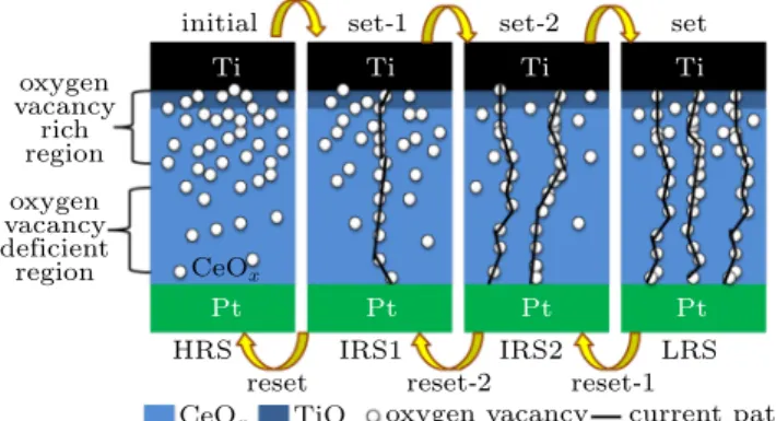
Based on the above analyses, the multilevel set and reset bipolar resistive switching in Ti/CeOx/Pt device is
schemati-cally illustrated in Fig.7. Multilevel set and reset character-istics can be well explained based on the nonstoichiometric distribution characteristics of oxygen vacancies in Ti/CeOx/Pt
device. CeO2is a material with multiple oxidation states (+3
and +4). The weak polycrystalline nature of ceria films may create variations in the lattice strain which could initiate inter-play between the two oxidation states resulting in the forma-tion of oxygen vacancies as a charge compensaforma-tion. In fact the formation energy at oxide surface is relatively low, so the concentration of oxygen vacancies at the surface can be ex-pected to be higher than that in the bulk of the sandwiched oxide.[26]Moreover, as Ti is capable to reduce CeO2so
prob-ability of a relatively richer density of oxygen vacancies near the Ti/CeOx interface is rather enhanced. While being nobel
metal, the bottom electrode (Pt) is incapable of creating an appreciable amount of oxygen vacancies near the Pt/CeOx
in-terface. The resulting non-uniform density of oxygen vacan-cies in the oxide layer leads to bipolar resistive switching in Ti/CeOx/Pt device. Furthermore, the formation of TiOxlayer
seems to play a significant role in the distribution and move-ment of oxygen vacancies as well as in the conductive filamove-ment formation/rupture. As fresh RRAM device needs the elec-troforming process before showing any reversible resistance switching. During forming process, the positive voltage stress applied at the top electrode pushes the positively charged oxy-gen vacancies from the TiO/CeOxinterface into the vacancy
deficient CeOxbulk to form separated line-pattern conductive
filaments. This happens because oxygen vacancies have abil-ity to distribute themselves in line-pattern between electrodes rather than an interconnected network of filaments and are sep-arated from one another due to impulsive interactions.[15,27,28] In the subsequent reset process, the negative bias applied to top electrode pulls oxygen vacancies back to the TiO/CeOx
inter-face from the bulk and oxygen ions towards the bulk, thus rup-turing the filament(s) as illustrated in Fig.7. The filamentary model explains the multilevel resistive switching mechanism as well. Because of the asymmetric distribution of oxygen va-cancies in the active oxide layer, a filament after its formation in the set step is not likely to increase in scale. That is why the resistance of the device with only one filament may be in-termediate until some additional filaments are formed at other locations when stronger biasing voltage is applied. The for-mation of multiple, and mutually separated, percolation paths
between the two electrodes switches the device from the inter-mediate resistance state to low resistance state. It is notewor-thy that if filamentary conduction paths were mutually con-nected (interconcon-nected network of filaments), there would be practically no difference in resistance levels of the LRS and the IRS. Ti Pt Pt Pt Pt Ti Ti Ti set-1 reset-1 reset-2
oxygen vacancy current path reset CeOx TiO CeOx set-2 set HRS initial oxygen vacancy rich region oxygen vacancy deficient region IRS1 IRS2 LRS
Fig. 7. (color online) Illustration of the proposed physical model to explain
bipolar switching mechanism in the CeOx-based RRAM device for the
mul-tilevel set and reset processes.
4. Conclusion
Nonstoichiometric CeOx-based memory device
suc-cessfully demonstrated multilevel set/reset bipolar resistive switching behavior. X-ray diffraction pattern confirmed that nature of the CeO2films is weak polycrystalline as well as the
formation of a thin TiO layer. The observed multilevel sta-ble intrinsic resistance states of CeOx could be attributed to
formation of separated line-pattern oxygen vacancy filaments in the CeOxfilm. The conduction mechanism in the LRS is of
Ohmic type, whereas in HRS it can be explained by Ohmic and trap-controlled space-charge-limited conduction dominated by Schottky emission. The reliability of resistive switching char-acteristics and data retention (104s) were also verified at room temperature. The multilevel resistive switching in Ti/CeOx/Pt
devices may be considered for multi-bit memory storage appli-cations. The highly stable switching behavior in Ti/CeOx/Pt
device has a great potential for nonvolatile memory applica-tions.
Acknowledgments
The authors acknowledge the financial support by Higher Education Commission (HEC), Islamabad Pakistan. The au-thors are also grateful to Prof. Dr. T. Y. Tseng, Department of Electronics Engineering and Institute of Electronics, National Chiao Tung University, Hsinchu, Taiwan for providing exper-imental facilities and useful suggestions.
References
[1] Tsai C T, Chang T C, Chen S C, Lo I, Tsao S W, Hung M C, Chang J
[2] Chen T C, Chang T C, Tsai C T, Hsieh T Y, Chen S C, Lin C S, Hung M
C, Tu C H, Chang J J and Chen P L2010 Appl. Phys. Lett. 97 112104
[3] Chen M C, Chang T C, Huang S Y, Chang K C, Li H W, Chen S C, Lu
J and Shi Y2009 Appl. Phys. Lett. 94 162111
[4] Chen Y C, Chang T C, Li H W, Chen S C, Lu J, Chung W F, Tai Y H
and Tseng T Y2010 Appl. Phys. Lett. 96 262104
[5] Chang T C, Jian F Y, Chen S C and Tsai Y T2011 Mater. Today 14 608
[6] Chen S C, Chang T C, Liu P T, Wu Y C, Lin P S, Tseng B H, Shy J H,
Sze S M, Chang C Y and Lien C H2007 IEEE. Electron Dev. Lett. 28
809
[7] Chen W R, Chang T C, Yeh J L, Sze S M and Chang C Y2008 Appl.
Phys. Lett.92 152114
[8] Ismail M, Huang C Y, Panda D, Hung C J, Tasi T L, Jeing J H, Lin C A, Chand U, Rana A M, Ahmed E, Talib I, Nadeem M Y and Tseng T Y2014 Nano-scale Res. Lett. 9 45
[9] Waser R and Aono M2007 Nat. Mater. 6 833
[10] Tseng T Y and Sze S M 2012 An Introduction to Nonvolatile Memo-ries, in Materials, Devices and Applications, ed. Tseng T Y and Sze S M (Am. Sci. Publ., CA, USA), Vol. 1, Chap. 1, pp. 1–9
[11] Park I S, Kim K R, Lee S and Ahn J2007 Jpn. J. Appl. Phys. 46 2172
[12] Kang Y H, Choi J H, Lee T I, Lee W and Myoung J M2011 Solid State
Commun.151 1739
[13] Panda D, Dhar A and Ray S K2010 J. Appl. Phys. 108 104513
[14] Acharyya D, Hazra A, Dutta K, Gupta R K and Bhattacharyya P2013
Semicond. Sci. Technol.28 125001
[15] Liu L F, Hou Y, Yu D, Chen B, Gao B, Tian Y, Han D D, Wang Y, Kang J F and Zhang X 2012 IEEE. International Conference on Electron De-vices and Solid State Circuit (EDSSC), December 3–5, 2012, Bangkok, pp. 1–3
[16] Sun X, Sun B, Liu L, Xu N, Liu X, Han R, Kang F, Xiong G and Pan T P2009 IEEE. Electron Dev. Lett. 30 334
[17] Yang Y C, Chen C, Zeng F and Pan F2010 J. Appl. Phys. 107 093701
[18] Younus A, Chu D and Li S2012 J. Phys. D: Appl. Phys. 45 355101
[19] Zhao T H, Wei F, Zhang X and Du J2013 Solid-State Electron. 89 12
[20] Kang Y, Verma M, Liu T and Orlowski M K2012 ECS Solid State Lett.
1 Q48
[21] Kim H D, An H M and Kim T G2012 IEEE. Trans. Electron Dev. 59
2302
[22] Chen C, Yang Y C, Zeng F and Pan F2010 Appl. Phys. Lett. 97 083502
[23] Pan T M and Lu C H2013 Mater. Chem. Phys. 139 437
[24] Kao K C and Huang W 1981 Electrical Transport in Solids (Oxford: Pergamon) Vol. 14, p. 150
[25] Kim H D, Yun M. J, Lee J H, Kim K H and Kim T G2014 Sci. Rep. 4
4614
[26] Cho B, Song S, Ji Y, Kim T W and Lee T2011 Adv. Funct. Mater. 21
2806
[27] Liu T, Verma M, Kang Y and Orlowski M K2013 IEEE. Electron Dev.
Lett.34 108
[28] Jameson J R, Gilbert N, Koushan F, Saenz J, Wang J, Hollmer S and