Boost DC-DC Converter with Charge-Recycling (CR)
and Fast Reference Tracking (FRT) Techniques for
High-Efficiency and Low-Cost LED Driver
Chun-Yu Hsieh
and Ke-Horng Chen
Department of Electrical and Control EngineeringNational Chiao Tung University
Hsinchu, Taiwan
Abstract—A charge-recycling (CR) technique and fast
reference tracking (DRT) are proposed for implementing a high efficiency and low cost RGB backlight module in color sequential notebook computers’ display. A RGB LED driver composed of an asynchronous 1.5MHz DC/DC boost converter with FRT and CR techniques was fabricated in TSMC 0.25µm BCD 40V to generate 17V for series red LEDs or 21V for 6-series green, or blue LEDs. The CR technique stores extra energy at the output node when the output voltage is switched from low to high voltage level and releases the reserved energy back to the output node at next period. Furthermore, the output voltage can be rapidly switched between two different voltage levels by FRT technique without wasting much power owing to the CR technique.
I. INTRODUCTION
The most popular and power-efficiency backlight module is white LED backlight in LCD panels. The reason is that the power dissipation can be reduced about 40% compared to conventional CCFL backlight module. However, the color filter still is needed and thus generates about 70~80% NTSC color gamut. It is important to decrease to the power consumption in backlight module due to the color filter. Fortunately, without the requirement of color filter in LCD panels, the color-sequential (MCS) algorithm [1] in Fig. 1 that effectively reduced color breakup and motion blur effects can saves much power consumption of the backlight module. The color gamut can be raised to about 110% NTSC and the power dissipation can be further reduced to only 40% of that with CCFL backlight module. Therefore, the LCD panels without color filter need a low cost and high efficiency RGB backlight driver to achieve a high quality image display.
Fig. 1. (a) The timing diagram of color sequential technique for color-filter-less LCD panel.
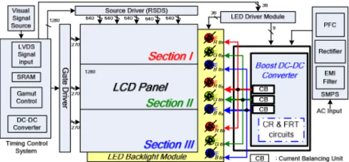
The MCS method displays three different colors of backlight in sequence in a period (1/60s). That is all LEDs are not needed to be turned on at the same time. However, the different colors of LEDs have different forward voltages due to the difference of LEDs between material and process. Therefore, nine boost converters in a RGB backlight module are demanded for notebook’s panel. Contrarily, if the output supplying voltage can be rapidly switched between 17V and 21V, we need only one DC-DC converter shown in Fig. 2 to drive RGB LEDs for implementing the modified MCS algorithm. For achieving high efficiency and low cost, charging recycling and fast reference tracking techniques are developed in this paper.
Fig. 2. The proposed LED driver with only one DC-DC converter in. A charge-recycling (CR) technique is proposed for save much power dissipation during the transition between two different output supplying voltages. Furthermore, in order to rapidly switch between two output voltages, a fast reference tracking (FRT) technique is presented in Section II. The circuit implementation is presented in Section III. The chip was fabricated in TSMC 0.25µm BCD 40V and experimental results are shown in Section IV. Finally, a conclusion is made in Section V.
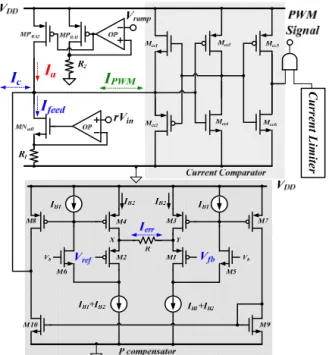
II. FAST REFERENCE TRACKING TECHNIQUE The LED driver for mixed color sequential algorithm needs two characteristics to meet the requirements of the LCD response time. One is the fast reference voltage tracking [2] for rapidly switching two different voltages between three colors and the other one is the charge recycling technique for reducing power consumption and improving the efficiency. Thus, the total schematic of the proposed RGB driver is shown in Fig. 3 (a).
(a) Gm Amplifier Ia Ifeed Ic ×Gm 1/r Current Limiter Current Comparator Sawtooth Generator sCVout Vfb Vref Vin PWM signals (b)
Fig. 3. (a) The proposed driver contains FRT, CR, and current balance unit (CB) circuits. (b) PWM generator with FRT technique.
A. Circuit of FRT technique
In Fig. 3 (b), the FRT technique for improving line transient speed needs a new current Ifeed that stands for the input voltage information. The definition of the peak value
IH=Vref*Gm of the saw-tooth generates a larger duty cycle to increase the output voltage quickly for fast tracking the variations of the reference voltage Vref. The duty cycle of a voltage-mode boost converter operated in continuous current mode (CCM) is defined as (1) and shown in Fig. 4. Ideally, the variation of Ic can be neglected compared to the variations of Ifeed.
0
( )
where
H feed c ref m feed o in H ref m H ref m I I I V G I V V D V I V G I V G − − × − − = = = × = × (1)
Fig.4. The determination of duty waveform in the FRT technique.
At steady state, the feedback voltage Vfb is equal to the reference voltage Vref is shown in (2) when the current Ifeed is used to minimize the variation of error current Ic. From (1) and (2), the expression of the duty cycle is rewritten as (3).
2 2 1 2 1 2 where F F ref fb o o F F F F R R V V V rV r R R R R = = = = + + (2) where o m feed o in feed in m o o m rV G I V V D I rV G V rV G × − − = = = × × (3)
Moreover, wideband Gm amplifier [3] is utilized to increase the system bandwidth. Besides, current limit circuit is also used to control peak current to make sure the correctly regulated output voltage. The circuit implementation is shown in Fig. 5. C u rr en t L im ite r
Fig. 5. The PWM generator with FRT technique consists of V-I converter, P compensator, and current comparator.
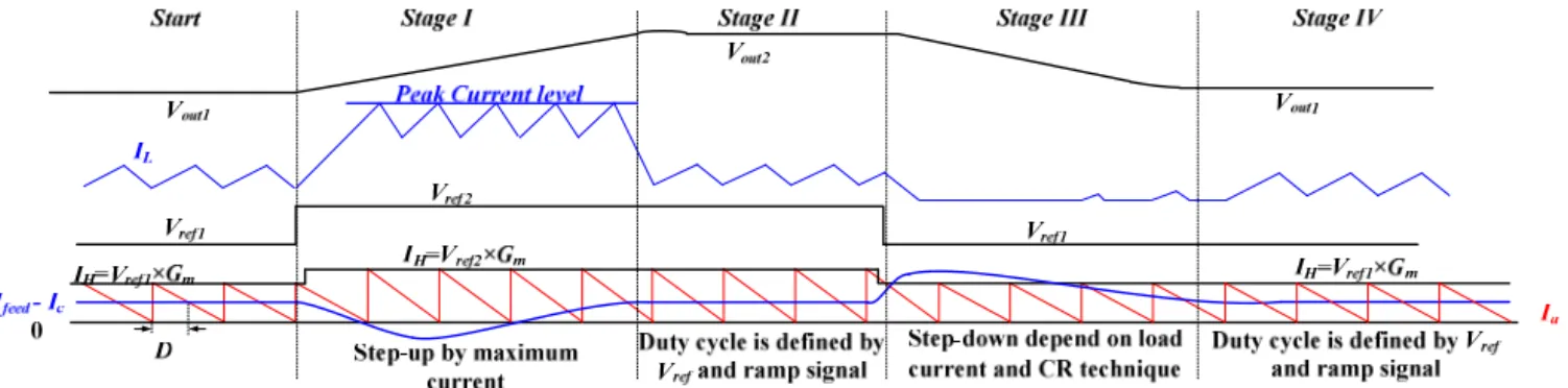
B. Analysis of FRT technique
The analysis of FRT operation is divided into four stages as follows and shown in Fig. 6.
Stage I: when the reference voltage Vref steps from Vref1 to
Vref2, the peak value IH of saw-tooth current Ia is increased instantly due to reference tracking mechanism. The error current Ic, which is the output of Gm amplifier, is also increased owing to a larger difference voltage between Vref to
Vfb. A feedforward current Ifeed is determined by input voltage
Vin. The difference current between Ifeed and Ic is compared to saw-tooth current Ia for determining duty cycle. Therefore, the summation current of Ifeed-Ic is decreased instantly as a result that reference voltage Vref is increased. Thus, by comparing Ia and Ifeed - Ic, the control signal VPWM is switched to a high level and the turn-on time of power transistor MN1 is limited to a predefined maximum duty that represents a peak current level. Thus, the boost converter is controlled by the peak current loop. The output voltage is raised to a high-supplying level for a forward conduction voltage of serial G or B LEDs within a short time [4-5].
Stage II: when the output voltage Vout approaches the high-supplying level, the error current Ic is gradually decrease by because the difference voltage between Vfb and
Vref is decreased. Owing to fast response of Gm amplifier, the current of Ifeed - Ic is increased rapidly. Thus, the PWM generator can substitute for the peak current control to circuit regulate the output voltage.
Fig. 6. The timing diagram of the proposed LED driver circuit with FRT technique. Stage III: when the reference voltage Vref is decreased instantly from Vref2 to Vref1, the error current Ic by Gm amplifier is instantly decreased owing to a larger difference voltage between Vref and Vfb. Besides, due to the reference tracking mechanism, the peak value of saw-tooth current Ia is decreased. Thus, the current Ia decreases and Ifeed-Ic increases instantly as well. By comparing Ia and Ifeed-Ic, the control signal VPWM can be adjusted to a lowest level to turn off power transistor MN1. Thus, the output voltage is decreased according to load current and the charge-recycling circuit as describe in Section III.
Stage IV: when the output voltage is decreased to the low-supplying level, the error current Ic is increased. Due to the fast response of Gm amplifier, the current of Ifeed-Ic is decreased instantly. The fast and stable pulse width control is guaranteed.
III. CRTECHNIQUE FOR IMPROVING EFFICIENCY The low-supplying level is quickly raised to the high-supplying voltage by the proposed FRT technique. However, the decreasing speed from high-supplying to low-supplying voltage depends on the output capacitor and load current. It is very hard to pull low the output voltage due to low load current. Therefore, the charge-recycling circuit redirects the extra charge from the output capacitor to the recycling capacitor CRe-cycle to maintain the high efficiency and rapidly pulls low the output voltage at the same time. When the mixed color sequential technique switch the different color LEDs, three signals (VclR, VclG, VclB) in Fig. 3 (a) and Fig. 7 determine the one-shot signal. If the Vout drops from high to low-supplying voltage, it enables a one-shot signal to turn on power transistor MP1. Thus, the charge-recycling circuit is activated and stores extra energy in the CRe-cycle. Besides, when Vout increases from low to high-supplying level to turn
Fig. 7. the circuit of charge recycling technique
on the G- or B-LEDs, the charge-recycling circuit discharges the CRe-cycle and the stored energy is used to speed up the raising time. Moreover, because VRe-cycle switches between high or low supplying level, the body select circuit is needed to prevent the forward biasing current from decreasing efficiency. The charge recycling circuit effectively saves much power when the backlight module changes from R-LEDs to G- or B-R-LEDs.
The LEDs backlight module needs two different voltage in the different time, and the difference voltage Vdiff is approximately 5V. Thus the charge-recycling circuit can transfer 5V energy from capacitor. Thus, the CRe-cycle is chosen a value like that of external of capacitor Cload. Owing to the laws of conservation of energy, the one-shot time is defined as (4). ( load or Re cycle) one shot tran C C V T I − − × = (4)
Itran is an average current in the transmitted energy period. The slope of inductor current is defined as Vdiff /LRe-cycle. The peak value of inductor current Ipeak is about 2 × Itran. Thus, the value of inductor is defined as (5).
/ 2
2 2
8
diff one shot
peak tran
Re cycle diff one shot Re-cycle tran V T V t I I L L V T L I − − − ∆ ⋅ = ⇒ ⋅ = ⋅ ⋅ ⇒ ≈ (4)
According to (4) and (5), the CR circuit is designed to smoothly transfer energy between two capacitors. The one shot signal is determined by VclR, VclG, and VclB. When the backlight module changes from G- or B- LEDs to R- LEDs, it sends one shot signal to turn on the power transistor MP1. At this time, the CR circuit is activated to transmit energy from Cload to CRe-cycle. Contrarily, when the backlight module changes from R- LEDs to G- or B- LEDs, the stored energy is restored back to Cload. However, when G- LEDs changes to B- LEDs, the CR circuit is not activated.
IV. EXPERIMENTAL RESULTS
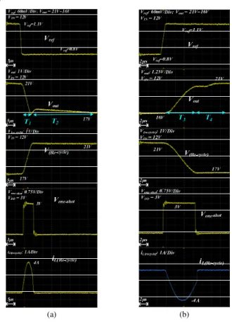
The proposed boost converter with charge recycling circuit was fabricated in 0.25µm TSMC BCD 40V process. When the output voltage changes from high-supplying level for G- or B- LEDs to low-supplying level for R- LEDs, a one-shot
signal is sent to turn on the power transistor for transmitting energy from Cload to CRe-cycle. The charge-recycling waveforms are shown in Fig. 8. In Fig. 8(a), the IL(Re-cycle) transmits energy from Vout to VRe-cycle and the energy stored in
CRe-cycle at time T1. The dropout voltage of Vout depends on the value of load capacitor Cload and load current at time T2.When the low-supplying level steps to high-supplying level, a one-shot signal is sent to restore the recycling energy. The stored energy in the CRe-cycle is transferred back to Vout for rapidly raising the output voltage. Thus, Fig. 8(b) shows the reversing current IL(Re-cycle) from VRe-cycle to Vout at time T3. The stored energy in CRe-cycle is released to speed up the transient time at the dynamic output voltage. The output voltage gets much energy from the CR circuit of boost converter at time
T4.
(a) (b)
Fig. 9. (a) When G- or B- LEDs switch to R-LEDs, the extra energy is stored in the auxiliary inductor L(Re-cycle) and capacitor CRe-cycle, which is triggered by
the one-shot signal. (b) When R-LEDs switch to G- or B- LEDs, the extra energy stored in the auxiliary inductor L(Re-cycle) and capacitor CRe-cycle is
released to the output node Vout, which is triggered by the one-shot signal.
Fig. 9. Chip micrograph.
Thus, the extra energy stored at the CRe-cycle is efficiently used to drive the LED arrays. The micrograph of the chip is shown in Fig. 9. Performance summary is listed in Table I.
Table I: PERFORMANCE SUMMARY
Input Voltage 8~13.5V Inductor 10 µH Output Voltage 16~21V Capacitor Cload=4.7 µF, CRe-cycle =4.7 µF, Switching frequency 1.5MHz Load Regulation 0.5mV/mA@VIN=12V, VOUT=21V Max. output current 300mA Line Regulation 1.36mV/V@VOUT=30V, IOUT=80mA V.CONCLUSIONS
A RGB LED backlight driver is proposed for rapidly switching between driving series R (about 17V) and 6-series G/B LEDs (about 21V). Owing to voltage difference about 4V between driving series-R and series-G/B LEDs, the FRT technique is presented to enhance line and load regulations. Besides, extra energy can be stored in a charge re-cycling capacitor at the transition from high voltage (21V) to low voltage (17V) while it can be restored back to output node to speed up the raising of voltage back 21V at the stage of driving G/B LEDs. The proposed LED driver with charge recycling circuit was implemented in 0.25µm TSMC BCD 40V process. Experimental results show that the transition time can be reduced within 22µs and the power consumption of the backlight module is smaller than 3W in Fig. 10.
Fig. 10. (a) The power consumption of LCD panel with color filter and CCFL backlight is larger than 5W. (b) The power consumption of the color filter-less LCD panel with the proposed RGB backlight driver is about 2-3W.
REFERENCES
[1] Yi-Fu Chen, Che-Chin Chen, and Ke-Horng Chen, “Mixed Color Sequential Technique for Reducing Color Breakup and Motion Blur Effects,” IEEE/OSA Journal of Display Technology, pp. 377-385, Dec. 2007.
[2] Man Siu, Philip K.T. Mok, Ka Nang Leung, Yat-Hei Lam, Wing-Hung Ki, “A voltage-mode PWM buck regulator with end-point prediction,” IEEE TCAS II, vol. 53, no. 4, pp. 294-298, April 2006. [3] Werner Hollinger, Manfred Punzenberger, “An Asynchronous
1.8MHz DC/DC Boost Converter Implemented in the Current Domain for Cellular Phone Lighting Management,” IEEE European
Solid-State Circuits Conference, pp. 528-531, Sep. 2006.
[4] Ke-Horng Chen, Hong-Wei Huang, and Sy-Yen Kuo, “Fast Transient DC-DC Converter with On-Chip Compensated Error Amplifier,” in
IEEE Transaction on Circuits and Systems II, pp. 1150-1154, Dec. 2007.
[5] Hong-Wei Huang, Chun-Yu Hsieh, Ke-Horng Chen, and Sy-Yen Kuo, “Adaptive Frequency Control Technique for Enhancing Transient Performance of DC-DC Converters,” IEEE European Solid-State
Circuits Conference, pp. 174-177, Sep. 2007.
[6] Doshi, Montu; Zane, Regan, “Digital Architecture for Driving Large LED Arrays with Dynamic Bus Voltage Regulation and Phase Shifted PWM” IEEE Applied Power Electronics Conference, pp.287-393, Feb. 2007.