IEEE ELECTRON DEVICE LETTERS, VOL. 33, NO. 1, JANUARY 2012 77
High-Performance Light-Erasable Memory and
Real-Time Ultraviolet Detector Based on
Unannealed Indium–Gallium–Zinc–Oxide
Thin-Film Transistor
Wei-Tsung Chen and Hsiao-Wen Zan
Abstract—A light-erasable memory and a real-time ultra-violet (UV) detector were developed from an amorphous indium–gallium–zinc–oxide (IGZO) thin-film transistor fabri-cated at room temperature without post-annealing. The natural defects within the IGZO or at the dielectric interface serve as electron traps to support a writing operation (switching down the channel conductance). A negative gate bias accompanied by UV illumination performs an erasing operation (switching up the channel conductance). After the writing/erasing of the proposed memory, an on/off ratio greater than 104 was maintained for a testing duration of 10 000 s. A real-time UV detector was also de-veloped, and a light/dark ratio of roughly 104was demonstrated.
Index Terms—Indium–gallium–zinc–oxide (IGZO), memory, photodetector and room temperature.
I. INTRODUCTION
A
MORPHOUS metal–oxide thin-film transistors such as amorphous indium–gallium–zinc–oxide thin-film tran-sistors (a-IGZO TFTs) are promising devices for uses in active-matrix displays, owing to their advantages such as high mobility [1] and low-temperature fabrication [2]. An a-IGZO TFT fabricated at low temperature exhibits an unstable thresh-old voltage under operation [3], [4]. Generally, efforts such as post-annealing and passivation are necessary to stabilize the a-IGZO TFT [4], [5]. The unstable behavior, however, can be advantageous when devices are used as detectors or memory. The threshold voltage (VTH) is easily shifted by a bias stress, thus satisfying the requirement of a memory.In this letter, based on the unstable characteristics of the a-IGZO TFT without post-annealing, we propose two promising applications: a light-erasable memory and a photodetector. In previous reports, a-IGZO TFTs with an additional carrier-trapping structure such as a floating gate [6], [7], a ferrodielec-tric [8], or a charge storage medium [9] have demonstrated good
Manuscript received September 19, 2011; revised September 30, 2011; accepted October 3, 2011. Date of publication November 8, 2011; date of current version December 23, 2011. This work was supported by the National Science Council (100-2628-E-009-018-MY3). The review of this letter was arranged by Editor P. K.-L. Yu.
The authors are with the Department of Photonics, Institute of Electro-Optical Engineering, and Display Institute, National Chiao Tung University, Hsinchu 300, Taiwan (e-mail: [email protected]).
Color versions of one or more of the figures in this letter are available online at http://ieeexplore.ieee.org.
Digital Object Identifier 10.1109/LED.2011.2171316
memory characteristics. In this letter, a conventional a-IGZO TFT without an additional carrier-trapping structure or post-annealing is proposed to serve as the memory device. The in-trinsic acceptorlike states facilitate a significant positive shift in
VTH, which supports the writing operation by providing the low channel conductance (low state) of a memory or photodetector. Generally, these defects are intentionally suppressed by post-thermal annealing [4]; however, for a memory or photodetector, these defects become usable trapping centers that are obtained without effort.
A metal–oxide material exhibits an intense ultraviolet (UV) photoresponse that partially depends on the oxygen in the surrounding environment [10]. The optical bandgap of a-IGZO is around 3.2 eV [11], which indicates that UV light with a wavelength shorter than 400 nm can be strongly absorbed by an IGZO film. In this letter, a negative gate bias (VG) accompanied
by UV illumination facilitates a significant negative shift in
VTH for the a-IGZO TFTs, through either hole trapping at the dielectric surface [12] or oxygen reemission from the exposed surface [10], which supports the erasing operation by provid-ing the high channel conductance (high state) of a memory. Furthermore, although the writing operation is promptly dis-abled when the UV illumination commences, the writing mech-anism also instantaneously recovers when the UV illumination ceases, and this facilitates its application in a real-time UV de-tector. The light-erasable memory is applicable in optical touch panels, while the sensitive UV detector based on the wide-bandgap IGZO is applicable, where blindness to visible light is required [10].
II. EXPERIMENTALPROCEDURE
A 100-nm-thick layer of thermal silicon nitride (SiNx) was
grown on heavily doped Si wafers to serve as the gate dielectric. A 35-nm-thick layer of a-IGZO was deposited on the SiNxat
room temperature by radio-frequency (RF) sputtering through a shadow mask to form the active layer. The RF power and the pressure were 70 W and 7 mtorr, respectively. The gas introduced during the sputtering was argon. Some devices were subjected to an annealing process at 350 ◦C in a nitrogen furnace for 1 h. Finally, as shown in Fig. 1(a), each bottom-gate top-contact a-IGZO TFT was completed with a 50-nm-thick layer of aluminum (Al) that was deposited through a shadow mask to form the source and drain contacts. The channel length 0741-3106/$26.00 © 2011 IEEE
78 IEEE ELECTRON DEVICE LETTERS, VOL. 33, NO. 1, JANUARY 2012
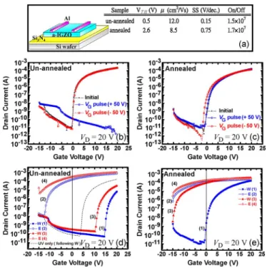
Fig. 1. (a) Schematic cross section of a-IGZO TFTs. (b) and (c) Transfer characteristics of unannealed and annealed a-IGZO TFTs as measured shortly after fabrication in response to positive VGpulse (50 V, 20 s) and negative VGpulse (−50 V, 20 s). (d) and (e) Transfer characteristics of unannealed and annealed a-IGZO TFTs as measured after several cycles of writing by positive VGpulse (50 V, 20 s) and erasing by negative VGpulse (−50 V, 20 s)
accompanied by UV illumination. The curves in blue and red are for the first and second write/erase cycles, respectively. The numbers (1)–(4) in the figure denote the operation sequence.
(L) and channel width (W ) of the device were fixed at 400 and 1000 μm, respectively. A low-pressure mercury lamp, whose main emission line had a wavelength of 254 nm, served as the UV light source. The power density on the surface of the sample was around 0.1 mW/cm2.
III. RESULTS ANDDISCUSSION
Fig. 1(b) and (c) shows the transfer characteristics of the a-IGZO TFTs as fabricated (unannealed) and when annealed, respectively. After annealing, the shallow acceptor states (tail states) are reduced. The degraded subthreshold slope (SS) after annealing may relate to the increase in deep states, but the mechanism requires further investigation. Both of the devices were subjected to measurements using a positive VG pulse
(50 V, 20 s) and a negative VG pulse (−50 V, 20 s). The
unannealed device exhibited great endurance under the nega-tive VG stress but high sensitivity to the positive VG stress,
which shifted the VTH beyond the scope of measurement. By contrast, the annealed device exhibited adequate stability under the positive VGstress but a slightly degraded stability under the
negative VGstress.
A post-annealing treatment can noticeably improve the sta-bility of IGZO TFTs by reducing the electron trap defects [4]. For the proposed light-erasable memory, the writing (increasing
VTH) and erasing (decreasing VTH) were performed using, respectively, a positive VG pulse (50 V, 20 s) unaccompanied
and a negative VG pulse (−50 V, 20 s) accompanied by UV
illumination. Fig. 1(d) and (e) shows, respectively, the transfer
Fig. 2. (a) Monitored IDof a-IGZO TFT after writing/erasing. (b), (c), and
(d) Endurance characteristics, data-retention characteristics, and write/erase speeds of the proposed memory.
characteristics of the unannealed and annealed devices after several writing/erasing cycles. For the unannealed device, the
VTH position can be controlled as required by either writing or erasing. As shown in Fig. 1(d), the unannealed device was: 1) placed in the low state by writing, 2) transferred to the high state by erasing, and 3) transferred back to the low state by writing. The difference in VTH between the low and high states (the VTH window) of the light-erasable memory was around 30 V. As shown in Fig. 1(e), the electron trap defects were decreased by thermal annealing, so the writing operation was invalid for the annealed device. That is, the annealed device can only be erased, not written, and therefore cannot serve as a memory. Furthermore, the dotted curve in Fig. 1(d) was obtained by applying UV illumination following a writing operation and shows that UV illumination alone can reduce the trapping of electrons. This property would be useful for application of the device in a photodetector.
Fig. 2(a) shows the duration characteristics of the light-erasable memory after writing (50 V, 20 s) and erasing (UV on, −50 V, 20 s). The drain current was monitored continu-ously for 10 000 s with VG= 0 and VD= 20 V. The channel
conductance produced by either writing or erasing could be well maintained for at least 10 000 s. An on/off ratio greater than 104 was recorded. Fig. 2(b) and (d) shows the endurance characteristics, data-retention characteristics, and write/erase speeds of the proposed memory, respectively. Before measur-ing the endurance characteristics, the UV intensity was tuned slightly to balance the responses of the writing and erasing operations. With a conventional a-IGZO TFT structure, the proposed memory device possesses a VTH window of around 10 V when the retention time is 10 000 s. The writing action is due not to the release of trapped holes but to the generation of additional trapped electrons. For annealed devices, the diffi-culty to generate trapped electrons makes the device unwritable. Because UV illumination of a-IGZO TFTs can suppress the effect of writing, a UV detector can be realized by operating
CHEN AND ZAN: LIGHT-ERASABLE MEMORY AND REAL-TIME UV DETECTOR BASED ON IGZO TFT 79
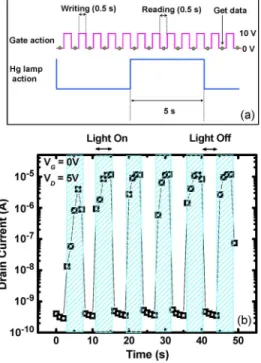
Fig. 3. (a) Action scenarios of VGand UV lamp. (b) Temporal evolution of IDfor a-IGZO under flashing UV illumination.
an a-IGZO TFT in a cycle that alternates between writing and reading. Writing is used to keep the conductance low during the period without the UV, which can promptly switch off the photocurrent. Fig. 3(a) shows the action scenarios of the VG
and the UV lamp. The VGof the IGZO TFT was periodically
switched to alternate between reading (VG= 0 V, 0.5 s) and
writing (VG= 10 V, 0.5 s). Meanwhile, the UV lamp was
flashed with a light period of about 5 s. Fig. 3(b) shows the tem-poral evolution of IDfor the IGZO TFT under the flashing UV
illumination, where IDwas recorded at the reading stage for a VDof 5 V. The proposed UV detector responded promptly to
each illumination change, with a light/dark ratio of 104. There have been many previous studies of UV detectors based on zinc oxide (ZnO). However, phototransistors generally exhibit lower real-time light/dark ratios [13], so high-performance devices (with light/dark ratios from 10 to 3× 10³) are realized only when complicated ZnO nanowires are used [14], [15].
A positive VG is applied to produce electron trapping [4] at
the dielectric surface, resulting in a positive ΔVTH. Abundant electron trap defects, which can serve as electron storage cen-ters, are intrinsically present in the as-deposited IGZO TFT. Furthermore, the trapped electrons can be untrapped by UV illumination. A negative VGaccompanied by UV illumination
is applied to produce hole trapping [12] at the dielectric surface, resulting in a negative ΔVTH. However, most trapped holes cannot be untrapped by a subsequent writing operation, which indicates that trapped holes and electrons may possibly coexist in the dielectric.
IV. CONCLUSION
This letter has proposed two potential applications for the a-IGZO TFT: a light-erasable memory and a real-time UV
de-tector. An a-IGZO TFT can be fabricated at room temperature without the burden of post-annealing, because the intrinsic de-fects serve as electron traps. A negative VGpulse accompanied
by UV illumination can be regarded as the erasing operation. A light-erasable memory was demonstrated that offered a VTH window of 30 V and exhibited an on/off ratio of 105. UV not only enhanced the effect of negative VG stress but also
suppressed the effect of positive VG stress. A real-time UV
detector was also demonstrated that operated in a mode of alternate writing and reading states and exhibited a light/dark ratio of 104.
REFERENCES
[1] M. Kim, J. H. Jeong, H. J. Lee, T. K. Ahn, H. S. Shin, J. S. Park, J. K. Jeong, Y. G. Mo, and H. D. Kim, “High mobility bottom gate InGaZnO thin film transistors with SiOxetch stopper,” Appl. Phys. Lett.,
vol. 90, no. 21, p. 212 114, May 2007.
[2] K. Nomura, H. Ohta, A. Takagi, T. Kamiya, M. Hirano, and H. Hosono, “Room-temperature fabrication of transparent flexible thin-film transistors using amorphous oxide semiconductors,” Nature, vol. 432, no. 7016, pp. 488–492, Nov. 2004.
[3] H. W. Zan, W. T. Chen, C. W. Chou, C. C. Tsai, C. N. Huang, and H. W. Hsueh, “Low temperature annealing with solid-state laser or UV lamp irradiation on amorphous IGZO thin-film transistors,” Electrochem.
Solid-State Lett., vol. 13, no. 5, pp. H144–H146, 2010.
[4] K. Nomura, T. Kamiya, M. Hirano, and H. Hosono, “Origins of threshold voltage shifts in room-temperature deposited and annealed a-In–Ga–Zn–O thin-film transistors,” Appl. Phys. Lett., vol. 95, no. 1, p. 013 502, Jul. 2009.
[5] J. K. Jeong, H. W. Yang, J. H. Jeong, Y. G. Mo, and H. D. Kim, “Origin of threshold voltage instability in indium–gallium–zinc oxide thin film transistors,” Appl. Phys. Lett., vol. 93, no. 12, p. 123 508, Sep. 2008. [6] A. Suresh, S. Novak, P. Wellenius, V. Misra, and J. F. Muth, “Transparent
indium gallium zinc oxide transistor based floating gate memory with platinum nanoparticles in the gate dielectric,” Appl. Phys. Lett., vol. 94, no. 12, p. 123 501, Mar. 2009.
[7] Y. S. Park, S. Y. Lee, and J. S. Lee, “Nanofloating gate memory devices based on controlled metallic nanoparticle-embedded InGaZnO TFTs,” IEEE Electron Device Lett., vol. 31, no. 10, pp. 1134–1136, Oct. 2010.
[8] S. M. Yoon, S. H. Yang, S. W. Jung, C. W. Byun, S. H. K. Park, C. S. Hwang, G. G. Lee, E. Tokumitsu, and H. Ishiwara, “Impact of interface controlling layer of Al2O3for improving the retention behaviors
of In–Ga–Zn oxide-based ferroelectric memory transistor,” Appl. Phys.
Lett., vol. 96, no. 23, p. 232 903, Jun. 2010.
[9] N. C. Su, S. J. Wang, and A. Chin, “A nonvolatile InGaZnO charge-trapping-engineered flash memory with good retention characteristics,”
IEEE Electron Device Lett., vol. 31, no. 3, pp. 201–203, Mar. 2010.
[10] C. Soci, A. Zhang, B. Xiang, S. A. Dayeh, D. P. R. Aplin, J. Park, X. Y. Bao, Y. H. Lo, and D. Wang, “ZnO nanowire UV photodetec-tors with high internal gain,” Nano Lett., vol. 7, no. 4, pp. 1003–1009, Apr. 2007.
[11] K. Nomura, T. Kamiya, H. Yanagi, E. Ikenaga, K. Yang, K. Kobayashi, M. Hirano, and H. Hosono, “Subgap states in transparent amorphous oxide semiconductor, In–Ga–Zn–O, observed by bulk sensitive X-ray photoelectron spectroscopy,” Appl. Phys. Lett., vol. 92, no. 20, p. 202 117, May 2008.
[12] H. Oh, S. M. Yoon, M. K. Ryu, C. S. Hwang, S. Yang, and S. H. K. Park, “Transition of dominant instability mechanism depend-ing on negative gate bias under illumination in amorphous In–Ga–Zn–O thin film transistor,” Appl. Phys. Lett., vol. 98, no. 3, p. 033 504, Jan. 2011.
[13] H. S. Bae, C. M. Choi, J. H. Kim, and S. Im, “Dynamic and static photore-sponse of ultraviolet-detecting thin-film transistors based on transparent NiOxelectrodes and an n-ZnO channel,” J. Appl. Phys., vol. 97, no. 7,
p. 076 104, Apr. 2005.
[14] B. H. Kind, H. Yan, B. Messer, M. Law, and P. Yang, “Nanowire ultra-violet photodetectors and optical switches,” Adv. Mater., vol. 14, no. 2, pp. 158–160, Jan. 2002.
[15] S. N. Das, K. J. Moon, J. P. Kar, J. H. Choi, J. Xiong, T. I. Lee, and J. M. Myoung, “ZnO single nanowire-based UV detectors,” Appl. Phys.