IEEE PHOTONICS TECHNOLOGY LETTERS, VOL. 20, NO. 10, MAY 15, 2008 803
Further Enhancement of Nitride-Based
Near-Ultraviolet Vertical-Injection Light-Emitting
Diodes by Adopting a Roughened Mesh-Surface
Chia-En Lee, Yea-Chen Lee, Hao-Chung Kuo, Senior Member, IEEE, Tien-Chang Lu, and
Shing-Chung Wang, Life Member, IEEE
Abstract—In this letter, the nitride-based near-ultraviolet (NUV)
vertical-injection light-emitting diodes (VLEDs) with roughened mesh-surface are proposed and demonstrated by a combination of pattern sapphire substrate, wafer bonding, laser lift-off, and chem-ical wet etching processes. With the help of adopting a roughened mesh-surface, the light–output power (at 350 mA) of the NUV-VLEDs could be further enhanced about 20% as compared with that of the conventional NUV-VLED.
Index Terms—Laser lift-off (LLO), roughened mesh-surface,
vertical-injection light-emitting diodes (VLEDs), wafer bonding.
R
ECENTLY, tremendous progress has been achieved in GaN-based blue, green, and ultraviolet (UV) light-emitting diodes (LEDs). High-brightness GaN-based blue and green LEDs have already been extensively used in outdoor displays, traffic lights, LCD backlight, and exterior automotive lighting, etc., and show a greater potential to replace incandescent bulbs and fluorescent lamps [1]. UV emitters are of interest for fluorescence-based chemical sensing, flame detection, optical storage, and a pumping source for exciting phosphor applications [2]. These nitride-based LEDs are also potentially useful for solid-state lighting. Although the blue/green LEDs are commercially available, it is still difficult to manufacture high-power UV LEDs. It can be ascribed to the sensitivity to dislocation and the total internal reflection effect which influence the total external quantum efficiency [3]–[6]. Today, laser lift-off (LLO) LEDs are demonstrated to be one of the high potential light-emitting devices to achieve high brightness operation due to its excellent thermal dissipation [7]. In addition, the surface roughness technique seems to have high probability to provide large enhancement due to random scattering from the roughened surface [8], [9]. Therefore, how to further reduce the dislocation density and improve the light extraction efficiency are important issues for fabricating high-performance UV LEDs. In this letter, the pattern sapphire substrate (PSS), wafer bonding, LLO, and chemical wet etchingManuscript received October 7, 2007; revised December 14, 2007. This work was supported in part by the MOE ATU program and in part by the National Science Council of the Republic of China (R.O.C.) in Taiwan under Contract NSC 95-2120-M-009-008 and Contract NSC 94-2215-E-009-082.
The authors are with the Institute of Electro-Optical Engineering, National Chiao Tung University, Hsinchu 300, Taiwan, R.O.C. (e-mail: hckuo@faculty. nctu.edu.tw).
Color versions of one or more of the figures in this letter are available online at http://ieeexplore.ieee.org.
Digital Object Identifier 10.1109/LPT.2008.921129
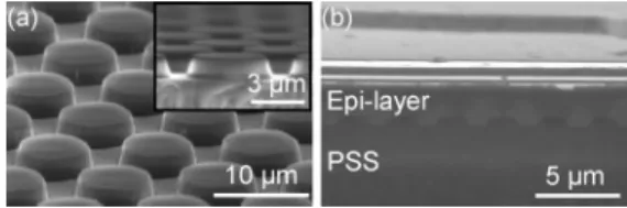
Fig. 1. SEM images of (a) PSS and (b) a GaN-based LED grown on a PSS.
surface treatment processes were implemented to fabricate the roughened mesh-surface near-UV vertical-injection LEDs (NUV-VLEDs) for further enhancement of NUV-VLEDs. Both internal quantum efficiency (IQE) and external quantum efficiency can be improved by the combination of crystal growth on PSS and VLEDs structure techniques. The electrical and optical properties of the roughened mesh-surface VLEDs will be reported.
The NUV-LED wafers used in this study were grown by low-pressure metal–organic chemical vapor deposition onto c-face (0001) 2-in diameter patterned and conventional sap-phire substrates at the same growth run. Fabrication of PSSs was illustrated as follows: The Ni film with bump-array pat-terns of 3- m diameter and 3- m spacing was deposited onto the sapphire substrate by e-beam evaporator and defined by standard photolithography to serve as the dry etching mask. The sapphire substrate was then dry etched using an induc-tively coupled plasma (ICP) etcher with an etching depth of 1 m. Fig. 1(a) shows the top and cross-sectional side views scanning electron microscope (SEM) images of the PSS. In this report, the NUV-LED structure comprised a 40-nm-thick GaN nucleation layer, a 2.0- m-thick undoped GaN layer, a 2.5- m-thick Si-doped n-type GaN cladding layer, an uninten-tionally doped active region of 405-nm emitting wavelength with five periods of InGaN–GaN multiple quantum wells, a 0.2- m-thick Mg-doped p-type GaN cladding layer, and a Si-doped n-InGaN-GaN short period superlattice struc-ture. Fig. 1(b) shows a cross-sectional SEM micrograph of a GaN-based LED grown on a PSS. According to Fig. 1(b), the PSS can be buried completely by a GaN epitaxial layer without appearance of void. By performing a detail comparison, both types of NUV-LED wafers with and without PSS were subjected to the VLEDs processes. Fig. 2 shows the diagrams of fabrication process for VLEDs. The fabrication process of VLEDs on Si began with the deposition of the highly reflec-tive ohmic contact layer Ni–Ag–Pt and Cr–Au bonding layer on p-GaN. Both types of samples were then bonded onto a
804 IEEE PHOTONICS TECHNOLOGY LETTERS, VOL. 20, NO. 10, MAY 15, 2008
Fig. 2. Diagrams of fabrication processes for VLEDs (a) wafer bonding, (b) LLO, and (c) chemical wet etching and electrode deposition.
Cr–Au-coated p-type conducting Si substrate at 350 C for 1 h to form the structure of sapphire (with and without PSS)/GaN LED/NiAgPt–CrAu–AuCr–Si [Fig. 2(a)]. The wafer bonded samples were then subjected to the LLO process to form the u-GaN (with and without mesh-surface)/n-GaN/MQW/p-GaN structure on Si [Fig. 2(b)]. A KrF excimer laser at a wavelength of 248 nm with a pulsewidth of 25 ns was used to remove the sapphire substrate. The incident laser with a beam size of 1.0 mm 1.0 mm was incident from the polished backside of the sapphire substrate onto the sapphire–GaN interface to decompose GaN into Ga and N. After removing the sapphire substrate, the sapphire-removed samples were dipped into HCl solution to remove the residual Ga on the u-GaN. The details of the LLO process are described in [7]. Then the u-GaN was etched away to expose the n-GaN layer by an ICP etcher. Then, a square mesa of 750 m 750 m was created by ICP for current isolation purposes. In order to further increase the light extraction efficiency of VLEDs, the top n-GaN sur-faces treated through a chemical etching using 40% KOH by weight dissolved in ethylene-glycol solution at 120 C for 120 s [10]. Finally, a Cr–Pt–Au electrode was deposited as the n-type contact and the VLEDs with and without mesh-surface was obtained [Fig. 2(c)]. The surface morphology of VLEDs was examined by SEM as shown in Fig. 3. It is obviously observed that the mesh-surface was naturally formed due to the epi-growth on PSS. According to Fig. 3(b), the hole-array mesh-surface of 3- m diameter, 3- m spacing, and 1- m depth shows a complementary structure from the PSS and was nearly crack-free. It indicates that the epi-layer was not adversely affected to device structure during the LLO process. Shown in Fig. 3(c) is an SEM image of the mesh-surface after KOH chemical etching at 120 C for 120 s.
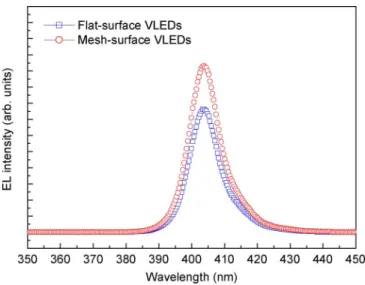
Notice that our roughened mesh-surface shows hexagonal cone-like features. Such a roughening surface can improve the escape probability of photons for luminance enhancement of VLEDs. Fig. 4 shows the room-temperature electrolumines-cence (EL) spectra of the flat-surface and mesh-surface VLEDs under 20-mA current injection. The EL peak positions of both the LEDs were located at 405 nm. The EL intensity of the mesh-surface LED is higher than that of the flat-surface one. This significant enhancement in EL intensity could be attributed
Fig. 3. SEM images of (a) surface morphology of mesh-surface VLEDs after LLO process, (b) cross-sectional view of VLEDs structure, and (c) mesh-surface VLEDs after chemical etching process.
Fig. 4. Room-temperature EL spectra of flat-surface and mesh-surface VLEDs.
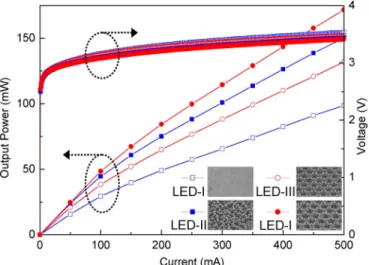
to the increase of the extraction efficiency by scattering the emission light from the mesh-surface. Additionally, it is be-lieved that the improvement in the IQE of the PSS LED [5], [11] could also contribute to the higher EL intensity of mesh-surface VLED. Current–voltage ( – ) and intensity–current ( – ) characteristics of four types VLEDs—conventional flat-surface VLEDs with (LED I) and without (LED II) chemical etching, mesh-surface VLEDs with (LED III) and without (LED IV) chemical etching—are shown in Fig. 5. It was found that the – curves were almost identical and similar ( 3.5 V at 350 mA) for these devices indicating that the fabrication
LEE et al.: FURTHER ENHANCEMENT OF NITRIDE-BASED NUV-VLEDs BY ADOPTING A ROUGHENED MESH-SURFACE 805
Fig. 5. L–I–V characteristics of flat- and mesh- surface VLEDs with and without chemical wet etching process.
processes would not result in any degradation in the electrical properties of nitride-based LEDs.
According to the corresponding – characteristics, four types of VLEDs showed linear characteristics up to 500 mA, indicating a good thermal dissipation management for the VLEDs’ structure design. It is clearly observed that the light output power of the LED-III was higher than those of LED-I. This result could be attributed to the increase of total external quantum efficiency by scattering the emission light from the mesh-surface and dislocation reduction of epi-growth on PSS. Furthermore, it is found that the light output power of meshed and flat surface VLEDs could be significantly raised from 100 mW (LED-III) to 130 mW (LED-IV) and 75 mW (LED-I) to 110 mW (LED-II) under 350-mA current injection, respectively, after chemical wet etching surface roughening process. We note that bare LED-IV (without an epoxy lens encapsulated) exhibit about 20% output power enhancement compared to that of LED-II. Such an enhancement can be as-cribed to the increase of surface emission area which improves the probability of photons escaping from semiconductor to air and the reduction of dislocation which increases the IQE by adopting the PSS. These two processes provide the roughened mesh-surface VLEDs with a significant further enhancement in output power compared to the conventional VLEDs.
In summary, the NUC-VLEDs with rough meshed-surface structure were investigated. The formation rough meshed-surface structure improves not only the surface emission area but the escape probability of photons due to the angular randomization of photos insides the LED structure. In addition, the IQE can be increased by adopting the PSS process. By this novel device design, the output power can be further enhanced up to 20%.
REFERENCES
[1] E. F. Schubert and J. K. Kim, “Solid-state light sources getting smart,”
Science, vol. 308, pp. 1274–1278, 2005.
[2] Y. Narukawa, I. NiKi, K. Izuno, M. Yamada, Y. Murazaki, and T. Mukai, “Phosphor-conversion white light emitting diode using InGaN near-ultraviolet chip,” Jpn. J. Appl. Phys., pt. 2 4A, p. L371, 2002. [3] K. Tadatomo, H. Okagawa, Y. Ohuchi, T. Tsunekawa, Y. Imada, M.
Kato, and T. Taguchi, “High output power InGaN ultraviolet light emit-ting diodes fabricated on patterned substrates using metal organic vapor phase epitaxy,” Jpn. J. Appl. Phys., vol. 40, pp. L583–L585, 2001. [4] M. Yamada, T. Mitani, Y. Narukawa, S. Shioji, I. Niki, S. Sonobe,
K. Deguchi, M. Sano, and T. Mukai, “InGaN-based near-ultraviolet and blue-light-emitting diodes with high external quantum efficiency using a patterned sapphire substrate and a mesh electrode,” Jpn. J. Appl.
Phys., vol. 41, pp. L1431–L1433, 2002.
[5] D. S. Wuu, W. K. Wang, W. C. Shih, R. H. Horng, C. E. Lee, W. Y. Lin, and J. S. Fang, “Enhanced output power of near-ultraviolet InGaN–GaN LEDs grown on patterned sapphire substrates,” IEEE
Photon. Technol. Lett., vol. 17, no. 2, pp. 288–290, Feb. 2005.
[6] Y. J. Lee, T. C. Hsu, H. C. Kuo, S. C. Wang, Y. L. Yang, S. N. Yen, Y. T. Chu, Y. J. Shen, M. H. Hsieh, M. J. Jou, and B. J. Lee, “Improve-ment in light-output efficiency of near-ultraviolet InGaN–GaN LEDs fabricated on stripe patterned sapphire substrates,” Mater. Sci. Eng., B, vol. 122, pp. 184–187, 2005.
[7] C. F. Chu, F. I. Lai, J. T. Chu, C. C. Yu, C. F. Lin, H. C. Kuo, and S. C. Wang, “Study of GaN light-emitting diodes fabricated by laser lift-off technique,” J. Appl. Phys., vol. 95, pp. 3916–3922, 2004.
[8] H.-W. Huang, C. C. Kao, J. T. Chu, H. C. Kuo, S. C. Wang, and C. C. Yu, “Improvement of InGaN–GaN light-emitting diode performance-with a nano-roughened p-GaN surface,” IEEE Photon. Technol. Lett., vol. 17, no. 5, pp. 983–985, May 2005.
[9] R. Windisch, C. Rooman, S. Meinlschmidt, P. Kiesel, D. Zipperer, G. H. Döhler, B. Dutta, M. Kuijk, G. Borghs, and P. Heremans, “Impact of texture-enhanced transmission on high-efficiency surface-textured light-emitting diodes,” Appl. Phys. Lett., vol. 79, pp. 2315–2317, 2001. [10] D. A. Stocker, E. F. Schubert, and J. M. Redwing, “Crystallor-gaphic wet chemical etching of GaN,” Appl. Phys. Lett., vol. 73, pp. 2654–2656, 1998.
[11] S. Watanabe, N. Yamada, M. Nagashima, Y. Ueki, C. Sasaki, Y. Ya-mada, K. Tadayomo, H. Okagawa, and H. Kudo, “Internal quantum ef-ficincy of highly-efficiect InGaN-based near-ultraviolet light-emitting diodes,” Appl. Phys. Lett., vol. 83, pp. 4606–4608, 1998.