國 立 交 通 大 學
電子工程學系電子研究所
博 士 論 文
新式位元層次設計方法及其應用於離散弦轉換
A Novel Bit-level Design Approach and its Application to Discrete
Sinusoidal Transforms
研 究 生 : 陳 漢 臣
指導教授 : 任 建 葳
張 添 烜
A Novel Bit-level Design Approach and its Application to Discrete
Sinusoidal Transforms
新式位元層次設計方法及其應用於離散弦轉換
研究生: 陳漢臣 Student: Hun-Chen Chen 指導教授: 任建葳 博士 Advisors: Prof. Chein-Wei Jen
張添烜 博士 Prof. Tian-Sheuan Chang
國立交通大學
電子工程學系電子研究所
博 士 論 文
A Dissertation
Submitted to Department of Electronics Engineering & Institute of Electronics College of Electrical and Computer Engineering
National Chiao Tung University in Partial Fulfillment of the Requirements
for the Degree of Doctor of Philosophy in
Electronics Engineering January 2006
推 薦 函
事由:推薦電子研究所博士班研究生陳漢臣提出論文以參加國立交通大學博士班 論文口試。 說明:本校電子研究所博士班學生陳漢臣已經完成本校電子研究所所規定之學科 課程及論文研究之訓練。有關學科方面,陳君已修畢十八學分(請查閱學籍 資料),通過學科考試。有關論文研究部份,陳君已完成「新式位元層次設 計方法及其應用於離散弦轉換」(A Novel Bit-level Design Approach and its Application to Discrete Sinusoidal Transforms)初稿。相關論文發表情形如下: [1]. H. C. Chen,J. I. Guo, T. S. Chang, and C. W. Jen, “A Memory EfficientRealization of Cyclic Convolution and its Application to Discrete Cosine Transform,” IEEE Tran. Circuits and Systems for Video Technology, vol. 15, no. 3, pp. 445-453, March 2005.
[2]. H. C. Chen, T. S. Chang, J. I. Guo, and C. W. Jen, “The Long Length DHT Design with a New Hardware Efficient Distributed Arithmetic Approach and Cyclic Preserving Partitioning,” IEICE Tran. Electronics, Vol. E88-C, No. 5, pp. 1061-1069, May 2005.
[3]. H. C. Chen, J. I. Guo, C. W. Jen, and T. S. Chang, “Distributed Arithmetic Realisation of Cyclic Convolution and Its DFT Application,” IEE Proceedings
Circuits, Devices and Systems, Vol. 152, No. 6, pp. 615-629, December 2005.
[4]. H. C. Chen, T. S. Chang, and C. W. Jen, “A Low Power and Memory Efficient Distributed Arithmetic Design and its DCT Application,” Proc. 2004 IEEE
Asia-Pacific Conference on Circuits and Systems, Tainan Taiwan, pp. 805-808,
2004.
[5]. H. C. Chen,J. I. Guo, and C. W. Jen, “A Memory Efficient Realization of Cyclic Convolution and its Application to Discrete Cosine Transform,” Proc.
2003 IEEE International Symposium on Circuits and Systems, Bankok Thailand,
pp. IV-33-IV-36, 2003.
[6]. H. C. Chen, J. I. Guo, and C. W. Jen, “A New Group Distributed Arithmetic Design for the One Dimensional Discrete Fourier Transform,” Proc. 2002 IEEE
International Symposium on Circuits and Systems, Arizona USA, pp.
I-421-I-424, 2002.
[7]. H. C. Chen, J. I. Guo, and C. W. Jen, “Low Power Module Designs for Video Codec Systems,” Proc. The 10th VLSI Design/CAD Symposium, Nantou Taiwan, pp. 275-278, 1999.
[8]. H. C. Chen, T. S. Chang, J. I. Guo, and C. W. Jen, “A Power-of-Two Variable Length DFT Processor using Group Distributed Arithmetic for Communication Applications,” submitted to IEEE Tran. Circuits and Systems I in Dec. 2005.
總言之,陳君具備國立交通大學電子研究所應有之教育及訓練水準,因此 推薦陳君參加國立交通大學電子研究所博士班論文口試。 此致 國立交通大學 電子研究所 電子研究所教授 任建箴 張添烜 中華民國九十四年十一月
新式位元層次設計方法及其應用於離散弦轉換
研究生: 陳漢臣 指導教授: 任建葳 博士 張添烜 博士 國立交通大學電子工程學系暨研究所 摘要 離散弦轉換已被廣泛的應用於數位信號處理,諸如: 影像處理、數位濾波器 及數位通訊等...。於低成本架構設計的研究,文獻中雖已有許多的設計,但都因 只考慮到係數的常數特性而未真正有效的著眼於不同演算法中這些係數的數值 特性,因此高效能低成本離散弦轉換之架構設計仍有極大的著墨空間。對此,本 論文提出了一低記憶體成本之位元層次設計方法並應用於高效能低成本之離散 弦轉換架構設計上。 本論文以迴旋疊積離散弦轉換演算法為基礎,同時利用分散式算數將輸入資 料分解至位元層次進而去除潛在的冗餘而提出名為群組式分散式算數之低記憶 體成本之位元層次設計方法;對於一個 N 點的迴旋疊積運算,所提出之新的分 散式算數設計方法僅僅使用了一組遠小於傳統式分散式算數設計方法的記憶 體、一組 N 位元之移位暫存器、及 N 個累加器。跟據輸入資料之迴旋特性,我 們重新安排了分散式算數架構中記憶體的內容進而消除了原先儲存於記憶體中 重複出現之係數和而達到降低硬體成本之目的。與傳統之分散式算數設計比較, 所提出之群組式分散式算數設計可使記憶體成本由O(2N) 降至 O(2N−log N2 );若 考慮額外付出的硬體代價,硬體成本則由O(2N) 改善至 O(2N−log2N +N +2)。 此外,為了使所提出之群組式分散式算數設計方法可應用於長點數之設計,群組 式分散式算數之分割問題是在提出一種新的分散式算數方法時必須面對的。對質 數點數及非質數點數我們分別結合了 Agarwal-Cooley 及 Pseudocirculant matrix factorization 等分割演算法進行迴旋疊積之分割,這樣的結合使得群組式分散式 算數設計方法在低成本長點數的迴旋疊積設計上一併得到了解決方案,也進而提 升了此二分割演算法在實際應用上之價值。換的設計中我們進一步利用了其中係數之對稱性,使得在群組式分散式算數之離 散傅利葉轉換設計上可再降低一半的記憶體成本。而在離散餘絃轉換的設計中, 由於迴旋疊積的不完美,為使群組式分散式算數方法能順利的應用於離散餘絃轉 換的設計之中,我們亦利用了離散餘絃轉換中係數之對稱性將原來的迴旋疊積演 算法轉換成一完美的迴旋疊積演算法,進而使得一個低成本的群組式分散式算數 離散餘絃轉換架構得以實現,這樣的一個處理也使得群組式分散式算數在離散餘 絃轉換的實現上亦減少了一半的記憶體成本。與現存的心脈式陣列架構及其他分 散式算數架構之離散絃轉換設計比較,所提出之群組式分散式算數架構可節省超 過 29% 的延遲時間-硬體成本乘積值。 考慮在通訊系統上的應用,本研究最後嘗試使用所提出之低硬體成本群組式 分散式算數設計方法來實現長點數且為可變點數之二的次方長度之離散傅利葉 轉換。我們使用 Cooley-Tukey 演算法先對離散傅利葉轉換進行分解,再使用 pseudocirculant matrix factorization 演算法對分解後的離散傅利葉轉迴旋疊積式 進行進一步的分割,使得一長點數的問題仍可利用低硬體成本之群組式分散式算 數加以實現。所提出之以群組式分散式算數設計為基礎的可變點數離散傅利葉轉 換架構可適用於 64/128/256/512/1024/2048/4096 等長度之離散傅利葉轉換。此 外,所提出之架構亦適用於任意長度之離散傅利葉轉換實現。與現存的長點數及 可變點數 FFT 架構比較,除了潛在延遲較短及高硬體使用率的優點外,在單位 產出率下,當長度小於 256 時,本架構可節省超過 9.6% 的硬體成本;因此, 所提出的是一個具相當競爭力的硬體架構實現。除了上述有關離散弦轉換的應用 外,本論文所提出之設計方法亦適用於任何有關迴旋運算的數位信號處理方面的 應用上。
A Novel Bit-level Design Approach and its Application to Discrete
Sinusoidal Transforms
Student: Hun-Chen Chen Advisors: Prof. Chein-Wei Jen Prof. Tian-Sheuan Chang
Department of Electronics Engineering and Institute of Electronics, National Chiao-Tung University
Abstract
The Discrete Sinusoidal transform (DSST’s) have been widely used in many digital signal processing applications such as image processing, digital filtering, digital communication, and etc. Although many designs of the DSST’s have been proposed in the literatures, their designs are still not efficient enough since they exploit only the constant property of the transform coefficients without considering the numerical property of these coefficients in the reformulated algorithms to further optimize the hardware cost. This dissertation proposes a novel bit-level hardware-efficient group distributed arithmetic (GDA) design and its applications for Discrete Sinusoidal transform (DSST’s) designs.
In the proposed GDA design approach, first we formulate the algorithm of DSST’s into cyclic convolution form in algorithm level. Then we use the distributed arithmetic to decompose the input data into bit-level in architecture level. Thus, the data redundancy due to the cyclic convolution can be efficiently removed within the bit-level input context to facilitate a hardware efficient DA realization. The proposed GDA approach rearranges the contents of DA memory according to its cyclic property such that redundancy of the contents can be eliminated and only a few groups of data are needed. Thus, compared with the conventional DA design, the memory cost of the proposed GDA design can be reduced from O(2N) to O(2N−log N2 ), and accounting with the necessary overhead, the overall complexity is improved from O(2N) to
) 2 2
( −log2 +N+
O N N
. To further extend its applications to long length designs, we further combine the Agarwal-Cooley algorithm and Pseudocirculant matrix factorization algorithm. This can partition the long length cyclic convolution into short ones while can still maintain its cyclic property, which avoids the non-cyclic problem of direct partitioning. Thus the proposed GDA design can efficiently be
applied to realize each of the shortened cyclic convolution blocks to achieve low hardware cost.
The proposed GDA design approach has been applied successfully to the DFT, DHT and DCT designs. For DFT design, we further combine the symmetrical property of the DFT coefficients with the proposed GDA design approach such that this design requires only half the contents to be stored. This further reduces the memory size by a factor of two. For the DCT design, in addition to the symmetry property of DCT coefficients, we further reformulate the non-cyclic DCT kernel into two perfect cyclic forms such that the DCT can be implemented by the GDA design approach with less hardware of (N-1)/2 adders or substractors, one much small memory module, a (N-1)/2-bit barrel shifter, and (N-1)/2+1 accumulators. Compared with the existing systolic array designs and DA-based designs, the realizations of 1-D DFT, DHT, and DCT with the proposed GDA design approach reduce the delay-area product more than 29% according to a 0.35 um CMOS cell library.
In addition to the prime length design, we also apply the GDA approach to the long length power-of-two DFT design commonly used in the communication system. We combine the proposed hardware efficient GDA approach with the Cooley-Tukey algorithm on DFT decomposition, and pseudocirculant matrix factorization algorithm on cyclic convolution partitioning to facilitate the long- and variable-length DFT design with low hardware cost. The proposed design can be flexibly used to compute the 1-D 64/128/256/512/1024/2048/4096-point DFT by cascading two 1-D short length DFTs and summing up the partitioned short length cyclic convolutions for each stage of the cascaded DFT. Besides, the proposed hardware efficient design approach can also be adopted in the design with the length beyond power of two. Compared with the existing long-length and variable-length FFT design, in addition to the advantages of short latency and high hardware utilization efficiency, under the same throughput rate, the proposed variable-length DFT can be a competitive design, and save the hardware cost more than 9.6% while the transform length is smaller than 256. In summary, the presented GDA-based design approach provides a solution to efficiently implement not only the DSST’s but also the DSP applications involving convolution and correlation.
CONTENTS
Chapter 1 Introduction...1
1.1 Motivation...1
1.2 Current status of DSST’s designs ...2
1.3 Review of DA-based designs...3
1.4 Overview of the proposed design approach...4
1.5 Considerations to the DSST’s designs ...5
1.6 Outline of this dissertation ...6
Chapter 2 The Group Distributed Arithmetic (GDA) Design Approach...8
2.1 Algorithm point of view...8
2.2 Architecture point of view ...10
2.2.1 Memory-based Group Distributed Arithmetic design...10
2.2.2 Analysis of Barrel shifter ...11
2.2.3 Evaluation of hardware cost...16
2.3 Consideration of low power design ...17
2.3.1 Analysis of transition activity ...17
2.3.2 Address morphing approach ...19
2.3.3 Exploration of dynamic range of the input data...20
2.3.4 Low Power Design with pre-computation scheme ...24
2.3.5 Evaluation of power cost ...28
2.4 Partitioning of cyclic convolution...29
2.4.1 Agarwal-Cooley algorithm...29
2.4.2 Pseudocirculant matrix factorization algorithm...30
2.4.3 Long length cyclic convolution design ...32
2.4.4 Evaluation of long length cyclic convolution GDA design ...37
Chapter 3 GDA-based Design for 1-D DSST’s ...39
3.1 Design of 1-D DFT ...39
3.1.1 Cyclic Convolution Formulation ...39
3.1.3 Symmetry exploration of the DFT in cyclic convolution ...45
3.1.4 Architecture design and evaluation ...49
3.2 Design of 1-D DHT ...57
3.2.1 Cyclic Convolution Formulation ...57
3.2.2 Numerical stability...59
3.2.3 Symmetry exploration of the DHT in cyclic convolution...60
3.2.4 Architecture design and evaluation ...64
3.3 Design of 1-D DCT...66
3.3.1 Cyclic Convolution Formulation ...66
3.3.2 Numerical stability...71
3.3.3 Architecture design and evaluation ...72
3.3.4 Chip implementation...79
Chapter 4 Long-length DSST’s designs ...80
4.1 Decomposition of long-length DSST’s ...80
4.1.1 Cooly-Tukey Algorithm ...80
4.1.2 Prime Factor Algorithm ...81
4.1.3 Rader’s Algorithm...83
4.2 Long length DHT Design and Evaluation...85
4.3 Variable-length DFT Design to Communication System Application...96
4.3.1 Overview of Communication system...96
4.3.2 Hardware Cost Analysis...97
4.3.3 GDA-based Variable Length DFT Design and Evaluation ...102
Chapter 5 Conclusion ... 118
5.1 Contributions... 118
5.2 Future Research Directions...119
List of Figures
Fig. 1.1: Outline of this research. ...7
Fig. 2.1: The proposed GDA architecture and the associated memory content arrangement in realizing the cyclic convolution example shown in (2.2)...10
Fig. 2.2: Multiplexer–based barrel shifter design...12
Fig. 2.3: Multiplier-based barrel shifter design. ...12
Fig. 2.4: Logarithmic number of multiplexer barrel shifter design. ...13
Fig. 2.5: Barrel shifter with N2 transistors...14
Fig. 2.6: Comparison of the four barrel shifters in (a) hardware cost, (b) power consumption, and (c) delay time. ...15
Fig. 2.7: The delay-area product comparison in the proposed GDA design and the traditional memory-based DA design with 16-bit data word length. ...17
Fig. 2.8: Trend of the improvement of transition probability versus the number of input-data bit...19
Fig. 2.9: The description of architecture transformation from DA to GDA ...20
Fig. 2.10: The test image with the size of 252 * 252 pixels. ...21
Fig. 2.11: gray-level of the pixels in the image of Fig. 2.10. ...22
Fig. 2.12: histogram of the gray-level distribution in the image of Fig. 2.10. ...22
Fig. 2.13: The preprocessed gray-level of the image in Fig. 2.10. ...23
Fig. 2.14: Histogram of the preprocessed data used in the example of 7-point DCT design...23
Fig. 2.15: The skipped bits in DA computation for the even outputs...25
Fig. 2.16: The skipped bits in DA computation for the odd outputs. ...26
Fig. 2.17: Power consumption of the GDA-based 1-D DCT designs. ...28
Fig. 2.18: The low cost version of BGDA design realizing the cyclic convolution example shown in (2.19). ...33
Fig. 2.19: The BGDA design on realizing the cyclic convolution example shown in (2.19) with high performance. ...34
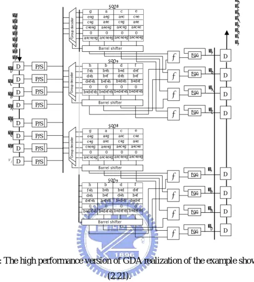
Fig. 2.20: The low cost version of GDA realization of the example shown in (2.21). ...36
Fig. 2.21: The high performance version of GDA realization of the example shown in (2.21). ...37
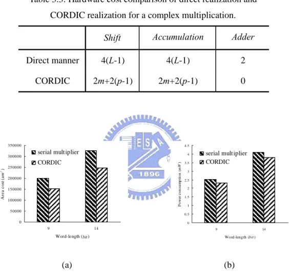
Fig. 3.1: Realization of CORDIC iterations and scaling iterations. ...44
Fig. 3.2: Comparison of (a) area cost and (b) power consumption for the complex multiplications realized with serial multiplier and CORDIC. ...45
Fig. 3.4: Comparison of the area cost of the existing DFT designs and the proposed GDA design in realizing the 1-D N-point DFT. ...53 Fig. 3.5: Comparison of the ACT for the existing designs and the proposed GDA
design in realizing the 1-D N-point DFT...54 Fig. 3.6: Comparison of the delay-area product for the existing designs and the
proposed GDA design in realizing the 1-D N-point DFT...54 Fig. 3.7: The architecture of the GDA design realizing the 1-D 11-point DHT. ...65 Fig. 3.8: The area reduction of the memory cost when applying the symmetry
property of DCT coefficients or not. ...69 Fig. 3.9: Block diagram of the proposed pipeline architecture for computing the 1-D
N-point DCT. ...73 Fig. 3.10: Design of the preprocessing stage in the 1-D 7-point DCT. ...74 Fig. 3.11: Design of the DA processing stage that is used to compute the kernel of
T((3k)7) in the 1-D 7-point DCT. ...74
Fig. 3.12: Design of the post-processing stage in the 1-D 7-point DCT including (a) the post-processing, and (b) the output buffer. ...76 Fig. 3.13: The delay-area product of the proposed design and the existing DCT
designs [33]-[35][52] in realizing the 1-D DCT...78 Fig. 3.14: Layout view of the 1-D 7-point GDA-based DCT design. ...79 Fig. 4.1: The GDA-based architecture design for 1-D 29-point DHT example ...90 Fig. 4.2: Comparison of the normalized area cost in the realization of 1-D N-point
DHT using the proposed design and the existing designs ...93 Fig. 4.3: Comparison of the normalized cycle time in the realization of 1-D N-point
DHT using the proposed design and the existing designs ...93 Fig. 4.4: Comparison of the normalized area-delay product in the realization of 1-D
N-point DHT using the proposed design and the existing designs ...94 Fig. 4.5: Average improvement of the normalized area-delay product in the designs
of 841-point DHT, 1653-point DHT, and 3249-point DHT using the proposed design approach ...95 Fig. 4.6: Transceiver /Receiver architecture in the communication system ...97 Fig. 4.7: Hardware cost of the original FFT versus the proposed GDA-based DFT 101 Fig. 4.8: Delay-area product of the FFT versus the proposed GDA-based DFT...102 Fig. 4.9: Block diagram of the proposed variable-length DFT architecture...104 Fig. 4.10: Architecture of 2-D DFT with real input...104 Fig. 4.11: Architecture design of the 2-D DFT in cyclic convolution formulation. .104 Fig. 4.12: Version 1 of the reduced architecture of 2-D DFT in cyclic convolution
formulation. ...105 Fig. 4.13: Version 2 of the reduced architecture of 2-D DFT in cyclic convolution
Fig. 4.14: Folding of the computation of each eight row blocks in 64-point cyclic convolution. ...106 Fig. 4.15: Folding of the computation of each four row blocks in 32-point cyclic
convolution. ...107 Fig. 4.16: Detail architecture of (a) the row 1-D DFT with input buffer and (b) the
column 1-D DFT with output buffer. ...109 Fig. 4.17: Detail design of (a) input buffer groups, (b) PISO groups, and (c) output
buffer groups in the proposed 1-D DFT architecture. ... 110 Fig. 4.18: (a) design of the 1-bit three dimensional rotator and the routing for (b)
2-bit BRG in stage 2, (c) 4-bit BRG in stage 3, and (d) 8-bit BRG in stage 4... 112 Fig. 4.19: Detail design of variable-length GDA-based module used for the
computation of Tij( ) in the proposed 1-D DFT architecture. ... 113
Fig. 4.20: Data-flow of the adder-group tree follows the GDAUs in the proposed variable-length DFT design. ... 114 Fig. 4.21: Detail design of serial multiplier groups in the proposed 1-D DFT
architecture. ... 115 Fig. 4.22: The transpose memory with the specific address generator... 115
List of Tables
Table 2.1: The rule of group mapping... 11 Table 2.2: Comparison of memory size in both the traditional memory-based DA and
the proposed GDA designs for different values of N. ...16 Table 2.3: Transformation of transition probability for the input data of the 4-input
data-path. ...18 Table 2.4: The relation ship of the address morphing...20 Table 2.5: Relationship between the sum of primary inputs and the even outputs...25 Table 2.6: Analysis for the covered lengths of cyclic convolution can be decomposed.
...30 Table 2.7: Comparison of the hardware cost of the design examples shown in
low-cost BGDA, high performance BGDA, and conventional DA in the case of non-coprime partitioning. ...38 Table 3.1: Table for θi ...43 Table 3.2: Determination of the si sequence at the θ of 56. ...43
Table 3.3: Hardware cost comparison of direct realization and CORDIC realization for a complex multiplication. ...45 Table 3.4: The 8 groups of memory content used for computing the 5-point cyclic
convolution in GDAUc...51 Table 3.5: The 8 groups of memory content used for computing the 5-point cyclic
convolution in GDAUs...51 Table 3.6: Area cost models to estimate the 1-D N-point DFT modules in the existing
systolic array designs, DA-based designs, and the proposed GDA design with real input data. ...55 Table 3.7: Area cost models to estimate the 1-D N-point DFT modules with the
partitioned cyclic convolution in the existing systolic array designs, DA-based designs, and the proposed BGDA design with real input data. ...56 Table 3.8: Average cycle time (ACT) models to estimate the not partitioned and
partitioned 1-D N-point DFT modules in the existing systolic array designs,
DA-based designs, and the proposed GDA design with real input data...57 Table 3.9: The 8 groups of memory content used for computing the 5-point cyclic
convolution in GDAUc...66 Table 3.10: The 8 groups of memory content used for computing the 5-point cyclic
convolution in GDAUs...66 Table 3.11: The seed-value, group address, and rotating factor used in the design of
group address decoder of 1-D 7-point DCT. ...75 Table 3.12: The partial products distribution for different DCT outputs under the
Table 3.13: 8-word memory contents arranged into groups. ...76 Table 3.14: The comparison of the proposed design and the existing DCT designs
[33]-[35][52] in realizing the 1-D N-point DCT in terms of delay and silicon area. 78 Table 4.1: Function of the address decoders in the 1-D 29-point DHT design... 91 Table 4.2: The performance comparison of different designs for computing the 1-D
N-point DHT ...92 Table 4.3: Length of 1-D DHT constructed by the decomposed short length DHTs..94 Table 4.4: The evaluation result of GDA-based DHT designs ...95 Table 4.5: DFT lengths for several communication systems ...97 Table 4.6: The computation complexity of various DFT algorithms...98 Table 4.7: The estimation of hardware costs of the FFT and the proposed GDA-DFT
...100 Table 4.8: The estimation of hardware costs of the FFT with actual complexity and
the proposed GDA-DFT ...100 Table 4.9: The estimation of cycle times of the FFT and the proposed GDA-DFT for
each sample ...101 Table 4.10: Length of 1-D DFT constructed by the decomposed short length DFTs103 Table 4.11: Condition of BR in each stage for DFT with the lengths of 64, 256, 1024,
and 4096. ... 111 Table 4.12: Comparison of the existing FFT designs and our DFT design ... 117
Chapter 1
Introduction
In this chapter, we illustrate the motivation, current status of DSST’s designs, review of the existing DA-based designs, overview of the proposed memory efficient bit-level design approach, considerations to the DSST’s designs, and outline of this dissertation. The details of the proposed design approach and associated advantage as well as the application in DSST’s will illustrate in the following chapters.
1.1 Motivation
The Discrete Sinusoidal transforms (DSST’s), including discrete Fourier transform (DFT), discrete Hartley transform (DHT), and discrete cosine transform (DCT), have been widely used in many digital signal processing applications such as image processing, digital filtering, digital communication, etc. There are two main solutions for realizing the high complexity of the DSST’s in real-time. One is based on the fast algorithms that aim at reducing the complexity of DSST’s to speed up the computation. The other is to directly realize the DSST’s formulations or their reformulations, such as the convolution, with hardware for accelerating the DSST’s computation.
The designs with fast algorithms are attractive for low computational complexity. However, hardware design of the algorithm is communication intensive and computation intensive to complicate the realizations of controller and arithmetic operation. In addition, most of the designs with fast algorithms exploit a butterfly datapath and a global memory in storing all of input/output data as well as the intermediate results. The mass data access from the global memory wastes a large percentage of power in this kind of designs. Besides, the cascaded structure in the fast algorithm makes the designs have poor numerical accuracy such that longer data word length in the datapath is needed. This fact will reduce the low complexity advantages of the fast algorithm and thus increase the hardware cost of the designs with fast algorithm, especially in the design with the length of non-power of two.
On the designs with direct manner, many existing architectures, such as the systolic array, are still severely suffered from large hardware cost because most of the
existing designs use area-consuming multipliers as the fundamental computing elements. Besides, these designs are not efficient enough since they only exploit the constant property of the transform coefficients without considering the possibility on further hardware optimization. Thus, efficient hardware design of the DSST’s is still a challenging problem due to its high computational complexity and the requirement of real-time processing.
The other popular architecture based on the distributed arithmetic (DA) has been adopted in DSP applications. In the case of short length, with less hardware cost, the memory-based DA design can instead of area-consuming multiplier for the computation of multiple-in-multiple-out (MIMO) inner product. Thus, trading the required performance, the DA technique shall be a hardware efficient method for the realization with direct manner. Combining with the good feature of DA, we explore the existing DSST’s algorithms to develop a hardware efficient DA design approach for real-time realization of the main modules in the multimedia and communication systems.
1.2 Current status of DSST’s designs
In this subsection, we will illustrate the current status of DSST’s designs with fast algorithms and the direct manner respectively.
For the DFT designs, the designs [1]-[5] exploited the feature of low computation complexity in fast Fourier transform (FFT) algorithms to achieve the goal of reducing the number of computation. However in these design, the global interconnection usually complicates the realization of controller. Since most of the FFT-based designs exploit a butterfly datapath and a global memory in storing all of input/output data as well as the intermediate results, the mass data access from the global memory wastes a large amount of power. Besides, the cascaded structure of FFT algorithm makes these designs have poor numerical accuracy such that longer data word-length in the data-path is needed. This fact will reduce the low complexity advantages of the FFT algorithm and thus increase the hardware cost of the FFT-based designs. On the exploration of hardware solution, the systolic array designs for DFT [6]-[11] were the major trend of realizing DFT in the past decades due to the promising VLSI features of modularity, locality, and regularity. However, these designs are still severely suffered from large hardware cost because most systolic array designs for DFT use
area-consuming multipliers as the fundamental processing elements (PEs).
For the Hartley transform (DHT) designs, since it is a good alternative to the discrete Fourier transform (DFT) for its real-number operations [12][13], the discrete Hartley transform (DHT) [14][15] also plays an important role in many DSP applications. There are many high-speed communication applications [16]-[21] that address the use of dedicated hardware designs for the DHT computation. For instance of the discrete multitone modulation (DMT)-based ADSL transceiver realization, the modulator and demodulator need to respectively compute the DFT and IDFT. The DFT and IDFT computation can be realized effectively by using DHT and IDHT computation for its inherent real-number operations [14]-[15]. The efficiency of using DHT to compute the DFT/FFT becomes more apparent in the applications encapsulating real input data than those encapsulating the complex input data. Many hardware implementations of the DHT have been proposed, including multiplier-based designs [22][23], Coordinate rotation digital computer (CORDIC)-based designs [14]-[29], memory-based designs [30][31], and hardwired multiplier-based design [32]. The design [22] uses a time recursive lattice structure to compute the 1-D DHT. The design [24] uses a fast algorithm to compute 1-D DHT. The designs [23][25]-[29] use direct matrix-vector multiplication algorithm to compute the 1-D DHT. The designs [30][32] use cyclic convolution based matrix-vector multiplication algorithm to compute the 1-D DHT.
For the DCT designs, due to playing a key function in image and signal processing, especially for the demanding multi-media and portable applications, the efficient hardware implementation of DCT is still a challenging problem for the requirements of high computational complexity and real-time processing. To achieve efficient hardware realization, except for the multiplier-based systolic array designs, many researches have been done on realizing the multiplications needed in the DCT through memory. One is the memory-based systolic array design [33] in which the proposed cyclic convolution based architecture possesses the features of simple I/O behavior and removes the data redundancy in the DCT coefficients.
1.3 Review of DA-based designs
To remedy the problems in the DFT, DHT, and DCT realizations with the designs mentioned above, many researches have realized the multiplications needed in
the DSST’s through memory [33]-[37]. One of the popular techniques is distributed arithmetic (DA). It has been widely used in many DSP applications such as the DSST’s, convolution, and digital filters [34]-[37]. The DA technique is an efficient method for computing inner products by using table look-up, shifting, and accumulations. Therefore, some existing designs are great interests in reducing the memory size required in the implementation of the DA-based architectures [34]-[36], such as the partial sum techniques and the Offset Binary Coding (OBC) techniques [34][35]. Besides, there is a different DA-based design denoted as adder-based DA design that realizes the multiplications by using adders instead of memories [32][38]-[40]. Chang [38]-[39] took advantage of the shared partial sum-of-products and sparse nonzero bits in the fixed input data to reduce the computational complexity. Guo [32][40] exploited the feature of cyclic convolution to simplify the computation of DHT and DFT, so that the multiplications and additions can be realized by using a small number of adders. On the algorithm point of view, these existing designs mentioned above, cyclic convolution-based designs have the good features of simple I/O behavior and reduction of coefficients redundancy in the 1-D DFT, DHT, and DCT. However, since they only exploit the constant property of the transform coefficients without considering the possibility on further hardware optimization with different DSST’s algorithms, they are still not efficient enough.
1.4 Overview of the proposed design approach
In this dissertation, we propose a new hardware efficient DA approach for the 1-D DSST’s design. The proposed approach can further reduce the memory size required in the traditional DA technique [34]. For a glance of the proposed DA design approach, first we formulate the algorithm of DSST’s into cyclic convolution form in algorithm level, and then exploit the distributed arithmetic to decompose the input data into bit-level in architecture level. Thus, the data redundancy due to the cyclic convolution can be efficiently removed within the bit-level input context to facilitate a hardware efficient DA realization.
Observing the cyclic convolution realized by DA technique, we find that different DSST’s outputs can be computed using the same DSST’s coefficients and the same input data samples with rotated order. If we directly realize the DSST’s in cyclic convolution using traditional DA technique, we find that N identical memory modules are used. It reveals a message that the redundancy still exists in the contents of the
memory, which implies that the memory utilization in this case is not good enough. Therefore, we intend to reduce the memory size by re-arranging the memory contents in different way. Combining with the cyclic property, we first group the candidates of DA inputs with rotated order as the same candidate, and then arrange the memory contents in this manner that the partial products for accumulating different DSST’s outputs according to the candidates being grouped together, and accessed simultaneously for the different outputs of DSST’s. The partial products arranged in a group should be rotated suitably before accumulating. With this way, the memory module contains only few groups of contents and only one memory module, instead of N identical memory modules needed in the computation of 1-D N-point DSST’s in conventional DA design. We named this proposed new DA design approach, Group Distributed Arithmetic (GDA).
Because of the inherent issue of DA-based design that the memory size increases exponentially as the length of input data increases, the partition issue must be regarded for long length DA design. In the conventional DA design, we can arbitrarily partition the input data of DA, and then sum up the partial sums from the different memory modules to achieve low hardware cost. Because of the necessity of cyclic preserving, the manner of arbitrarily partitioning cannot be applied to the proposed GDA design. Otherwise, the benefit of low hardware cost in GDA design will not exist. To solve the problems mentioned above, we combine several algorithms to decompose the long length DSST’s and partition the DA design in each of the shortened DSST’s into smaller ones, which is still preserving the property of cyclic, such that the DSST’s can efficiently be realized with GDA design. In the proposed decomposition approach, we decompose the long length DSST’s into the short ones with prime factor algorithm (PFA) or Cooley Turkey algorithm, and further partition each of them by using Agarwal-Cooley algorithm [41] or pseudocirculant matrix factorization algorithm (PMFA) [42] such that all the partitioned short DSST’s are still composed of the shortened cyclic-convolution blocks. For such long-length computations, dedicated hardware designs can meet both the real-time and low hardware cost requirements in the various high-speed data communication applications.
1.5 Considerations to the DSST’s designs
coefficients for further reducing the hardware cost of the memory by a factor of two. Compared with the existing systolic array designs and DA-based designs, the DFT design with the proposed GDA design approach can reduce the delay-area product from 29% to 68% according to the 0.35 μm CMOS cell library for short lengths. As compared with the existing designs, the DHT design with the proposed GDA design approach possesses better performance in reducing the area-delay product from 52% to 91%. For the DCT design, due to the rotated input data in the input-data matrix of DCT possess different signs, it is not easy to apply the GDA approach directly to DCT realization. Exploiting the symmetry property of DCT coefficients, we merge the elements in the matrix of DCT kernel, and separate the matrix to two perfect cyclic forms. Then these two smaller perfect cyclic convolution forms can be realized with the proposed GDA approach. This realization facilitates reducing the memory size significantly. As compared with the existing DA-based designs, for an example of 1-D 7-point DCT with 16-bit coefficients; the proposed design can save more than 57% of the delay-area product. Besides, the 1-D DCT chip was implemented to illustrate the efficiency associated with the proposed approach.
As for the popular application of DFT with the length of power of two in the communication system, combining the proposed low cost GDA design with the suggested long-length transform decomposition methodology, a variable-length DFT design has been proposed and implemented in our studies. The proposed design can flexibly be used to compute the 1-D 64/128/256/512/1024/2048/4096-point DFT by cascading two 1-D short length DFTs and summing up the partitioned short length cyclic convolutions for each stage of the cascaded DFT. Besides, the proposed hardware efficient design approach can also be adopted in the design with the length beyond power of two. Compared with the existing long-length and variable-length FFT design [67]-[70], in addition to the advantages of short latency and high hardware utilization efficiency (HUE), the proposed variable-length DFT design can achieve competitive hardware cost under the same throughput rate.
1.6 Outline of this dissertation
The dissertation is organized following the research outline as Fig. 1.1. In chapter 2 we illustrate the proposed GDA design approach for cyclic convolution in detail, including the issue of cyclic convolution partitioning, and its advantages compared with the traditional memory-based DA approach on hardware cost and power
consumption points of view. Chapter 3 illustrates GDA for 1-D DSST’s designs, where the optimization on algorithm level for further reducing the hardware cost is involved. Chapter 4 illustrates long-length issues for DSST’s design and the proposed variable-length DFT design to communication Application. Finally, we conclude this dissertation in chapter 5, including contributions in this research and some future research directions. GDA DFT DHT DCT Long-length GDA (BGDA) Variable-length DFT Long-length DHT Long-length DFT •SA-DCT • Variable-length FFT • Unified DFT/IDFT Ch2 Ch2 Ch3 Ch4 Ch4 Ch4 Future work
Chapter 2
The Group Distributed Arithmetic (GDA)
Design Approach
The presented Group Distributed Arithmetic (GDA) design approach mainly consists of cyclic convolution and memory-based DA technique. The algorithm in cyclic convolution can significantly reduce the complexity for the inner product computation with multiple inputs and multiple outputs (MIMO). In the following, we illustrate the proposed GDA design approach from algorithm-level to architecture-level involving the solution of cyclic convolution partitioning for GDA design and the evaluations of hardware cost and power consumption for design with this approach.
2.1 Algorithm point of view
Let us first consider a cyclic convolution example:
,
4 3 2 1 4 3 2 1⎥
⎥
⎥
⎥
⎦
⎤
⎢
⎢
⎢
⎢
⎣
⎡
⋅
⎥
⎥
⎥
⎥
⎦
⎤
⎢
⎢
⎢
⎢
⎣
⎡
=
⎥
⎥
⎥
⎥
⎦
⎤
⎢
⎢
⎢
⎢
⎣
⎡
=
v
v
v
v
a
d
c
b
b
a
d
c
c
b
a
d
d
c
b
a
u
u
u
u
U
(2.1)where {v1, v2, v3, v4} are input data, {a, b, c, d} are coefficients, and {u1, u2, u3, u4}
are output data. Using the commutative property of convolution, we can rewrite (2.1) as follow:
⎥
⎥
⎥
⎥
⎦
⎤
⎢
⎢
⎢
⎢
⎣
⎡
⋅
⎥
⎥
⎥
⎥
⎦
⎤
⎢
⎢
⎢
⎢
⎣
⎡
=
⎥
⎥
⎥
⎥
⎦
⎤
⎢
⎢
⎢
⎢
⎣
⎡
=
d
c
b
a
v
v
v
v
v
v
v
v
v
v
v
v
v
v
v
v
u
u
u
u
U
3 2 1 4 2 1 4 3 1 4 3 2 4 3 2 1 4 3 2 1 . (2.2)Observing (2.2), we find that different outputs in vector U can be computed using the same input data with rotated order and the same set of coefficients {a, b, c,
d}. According to the DA technique [34], using the same set of coefficients implies that
same inputs with rotated order implies that we can arrange the partial products generated by them as a group and these partial products can be accessed simultaneously in accumulating all the outputs.
For facilitating utilization of the GDA design approach, the general form of GDA shows as
N
k
u
u
u
L q q q R k R k k N q N2
,
1
,
2
,
,
1 1 , 1 ) 1 ( 0 , 1 ) 1 ( 0+
⋅
=
L
−
=
− − = − + + + + −∑
(2.3) Whereu
R0,0=
R(
u
0)
,}
,
,
,
,
,
{
(0 ) 1,0 (1 ) 1,0 ( 1 ) 1,0 ( 1 ) 1,0 0 0 0 0 0 , 0=
+ N+ + N+ − + N+ − + N+ Ru
Ru
Ru
k Ru
N Ru
L
L
,}
,
,
,
,
,
{
1,0 2,0 ,0 ,0 0u
u
u
ku
Nu
=
L
L
and)
u
R(
u
Rq,q=
q ,}
,
,
,
,
,
{
(0 ) 1, (1 ) 1, ( 1 ) 1, ( 1 ) 1, ,q Rq N q Rq N q k Rq N q N Rq N q q Ru
u
u
u
u
=
+ + + +L
− + +L
−+ + ,}
,
,
,
,
,
{
u
1,qu
2,qu
k,qu
N,qu
q=
L
L
, and 1 0 , 1 ) ) 1 ( ) 1 (( 0 ,∑
0 = − + − + +⋅
=
N n n R k n kv
c
u
N and 1 , 1 ) ) 1 ( ) 1 (( ,∑
= − + − + +⋅
=
N n n q R k n q kv
c
u
N q .where L denotes the word length of the input data v, N denotes the length of cyclic convolution, Rq denotes the rotating factor for qth bit that is used for indicating the
number of position of the partial products in DA input and output should be rotated, and cn are the coefficients. The rotation function R( ) is used to rotate the elements in
the output vector
u
Rq,q from the input vectorv
Rq,q by Rq for the qth bit of DAcomputation. In the example of 4-point cyclic convolution mentioned above, the
2.2 Architecture point of view
2.2.1 Memory-based Group Distributed Arithmetic design
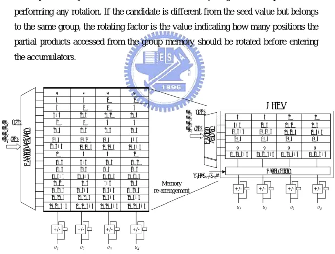
Fig. 2.1 shows the proposed GDA architecture for computing the vector U in (2.2). We arrange the memory contents (16 words) into six groups in this example. The candidate of DA input in the q-th bit, i.e. vector Vq, is first fed into an address decoder
to generate the group address Vq’ and the corresponding rotating factor Rq according
to the rule of group mapping shown in Table 2.1 that performed by the specific address decoder in the proposed GDA design when realizing the cyclic convolution example shown in (2.2). Here, the group address Gq denotes which group the
candidate of DA input belongs to. If the candidate is the seed value of a group V’q, the
rotating factor is equal to 00. That means the partial products accessed from the group memory is directly fed into the accumulators for computing the DA outputs without performing any rotation. If the candidate is different from the seed value but belongs to the same group, the rotating factor is the value indicating how many positions the partial products accessed from the group memory should be rotated before entering the accumulators. +/-u1 u2 u3 u4 a+b+c+d a+b+c+d a+b+c+d a+b+c+d +/- +/- +/-b c d a b+c+d c d a b a+d a+b b+c c+d d a b c a b c d 0 0 0 0 a+d a+b b+c c+d a+d a+b c+d b+c a+d c+d b+c a+b
a+b+c a+b+d a+c+d
a+b+c a+b+d a+c+d b+c+d
a+b+d a+c+d b+c+d a+b+c
a+c+d b+c+d a+b+c a+b+d
a+c b+d a+c b+d a+c b+d a+c b+d v1,q (msb) v2,q v3,q v4,q (lsb) Barrel shifter a+b+c+d a+b+c+d a+b+c+d a+b+c+d b+c+d a+d a+b b+c c+d a b c d 0 0 0 0
a+b+c a+b+d a+c+d
a+c b+d a+c b+d +/-u1 u2 u3 u4 +/- +/- +/-Rq={r1,q, r2,q} Memory re-arrangement Ad dres s de code r v1,q (msb) v2,q v3,q v4,q (lsb) Addre ss de co de r GDAU
Fig. 2.1: The proposed GDA architecture and the associated memory content arrangement in realizing the cyclic convolution example shown in (2.2).
Table 2.1: The rule of group mapping.
Grouped candidates of DA input (Vq) {v1,q, v2,q, v3,q, v4,q} Seed value (V’ q) {v’1,q, v’2,q, v’3,q, v’4,q} 1Rotating factor (Rq) {r1,q, r2,q } Group address (Gq) {g1,q, g2,q, g3,q} 0001 0 0010 1 0100 2 1000 0001 3 000 0011 0 0110 1 1100 2 1001 0011 3 001 0111 0 1110 1 1101 2 1011 0111 3 010 0101 0 1010 0101 1 011 0000 0000 0 100 1111 1111 0 101 Note:
1. Rotating factor denotes the number of position of the output data, corresponding to the candidate of DA input value in a group, needs to rotate.
2.2.2 Analysis of Barrel shifter
In this subsection, we will illustrate the hardware cost of barrel shifter in the design of overhead. Four barrel shifter designs are respectively analyzed and evaluated in the following. Fig. 2.2 shows the architecture realized with multiplexer. This straight forward design adopts the multiplexers that switch the input data to the selected outputs by the control signals as a rotation operation. The hardware required of this design is N times of N log2N+1-input AND gates and one N-input OR gates.
Thus the complexity of hardware is O(N2log2(log2N+1)+log2N) in gate count. It
reveals that the design with this approach is not hardware efficient. Besides, the number of level of the multiplexer logic will increase while the number of input is increased. Then the delay time in this design will be not a constant.
Fig. 2.2: Multiplexer–based barrel shifter design.
Fig. 2.3 shows the second design of barrel shifter. It adopts the multiplier with double length of input data. The duplicated input data is multiplied by the control signals, and then select out the 2nd N-bit of the result of multiplier as the shifted result. Although implementation with this algorithm uses only one multiplier and one-to-four demultiplexer, the word length in them is the drawback in hardware implementation. The required hardware in this design is one 2N-bit multiplier and one N-bit one-to-four demultiplexer. It is equivalent to 103*(-0.039 + 0.457 * 2N + 0.001 * 2N + 0.263 * 4N2)/58 and 2N 2-input gates (i.e., N * 2 2-input gate). Thus the complexity of hardware is O(N2+2N) in gate count .
Fig. 2.4 shows the third design of barrel shifter. This design consists of log2N rotators
and log2N N-bit two-to-one multiplexer. The length of these rotators are respectively
20, 21, …. 2log2N−1. If the length of the barrel shifter is not power of two, the length of
most significant rotator is N- (2log2N−2+2log2N−3+ … +20). Since each of the rotators
can be realized with the manner of wiring, there is no hardware cost on these rotators. Therefore, the hardware cost of this barrel shifter design is log2N N-bit two-to-one
multiplexer. It is equivalent to log2N times of 2N 2-input AND gates and N 2-input
OR gates. Thus the complexity of hardware is O(3Nlog2N) in gate count.
Fig. 2.4: Logarithmic number of multiplexer barrel shifter design.
Fig. 2.5 shows the fourth design of barrel shifter. This design consists of N2 transistors and N inverter gates. The hardware cost of this barrel shifter design is equivalent to N2/4+N/2 in gate count. Thus the complexity of hardware of this design is O(N2/4+N/2) in gate count. Compared with the designs mentioned above, it reveals that this design is the most efficient choice for the case that the length of input data is smaller than 64.
A[0] A[1] A[2] A[3] A[4] B[0] B[1] B[2] B[3] B[4] Sh[0] Sh[1] Sh[2] Sh[3] Sh[4] Sh[1] Sh[2] Sh[3] Sh[4]
Fig. 2.5: Barrel shifter with N2 transistors
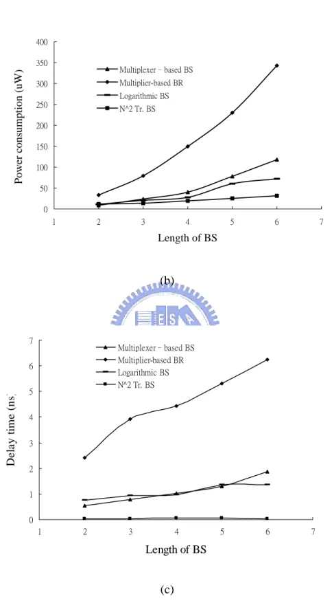
Fig. 2.6 (a), (b), and (c) show the comparisons of the four barrel shifters in hardware cost, power consumption, and delay time, respectively. It is seen that the area cost, power consumption, and delay time of N2-transistor barrel shifter are almost smaller than the others. However, this design is hard to implement by synthesis in the cell-based design flow. Thus the alternative of logarithmic barrel shifter is chosen, and synthesized in the implementation of the proposed GDA design and its applications.
0 2000 4000 6000 8000 10000 12000 14000 16000 18000 20000 1 2 3 4 5 6 7 Length of BS Area (u m 2 ) Multiplexer–based BS Multiplier-based BR Logarithmic BS N^2 Tr. BS
(a) 0 50 100 150 200 250 300 350 400 1 2 3 4 5 6 7 Length of BS Powe r c onsumption (uW) Multiplexer–based BS Multiplier-based BR Logarithmic BS N^2 Tr. BS (b) 0 1 2 3 4 5 6 7 1 2 3 4 5 6 7 Length of BS De la y t im e ( n s) Multiplexer–based BS Multiplier-based BR Logarithmic BS N^2 Tr. BS (c)
Fig. 2.6: Comparison of the four barrel shifters in (a) hardware cost, (b) power consumption, and (c) delay time.
2.2.3 Evaluation of hardware cost
In the following, we evaluate the delay time and hardware cost of the designs with the proposed GDA approach and the traditional DA approach for illustrating the advantages of the proposed approach. For a fair comparison, we adopt Avant 0.35μm CMOS cell-library [43] in the performance evaluation. The delay time for accessing a partial product from a memory module is taddr_dec + trom_acc in the traditional DA
designs, and taddr_dec + trom_acc + tbar_shf in the GDA design, where taddr_dec denotes the
delay time of address decoder, trom_acc denotes the access time of memory, and tbar_shf
denotes the delay time of the barrel shifter. Since the memory size required in the GDA design is much smaller than that in the traditional DA design, the delay time of address decoder and access time of memory in the GDA design are accordingly much smaller than that in the traditional DA design. However, the extra delay time of the barrel shifter must be counted in the GDA design. As a result, the total delay of the GDA design is almost similar to that of the traditional DA design. As for the hardware cost evaluation, the hardware for accessing a partial product is Arom in the traditional
DA design, and is Agrp_rom + Abar_shf in the proposed GDA design, where Agrp_rom
denotes the area cost of Group memory, and Abar_shf denotes the area cost of a barrel
shifter.
Table 2.2: Comparison of memory size in both the traditional memory-based DA and the proposed GDA designs for different values of N.
Length of cyclic convolution
(N) 3 4 5 6 7 8 9 10 11 12 13 14 …
Traditional DA 23 24 25 26 27 28 29 210 211 212 213 214 …
GDA
(# of group: G(N)) 4 6 8 14 20 36 60 108 188 352 632 1197 …
memory size reduction ratio
(DA / GDA) 2 2.7 4 4.6 6.4 7.1 8.5 9.5 10.9 11.6 13 13.7 …
Table 2.2 shows the comparison of memory size required in the two designs under different N. We can see that the proposed GDA design is much more hardware efficient than the traditional DA design. Fig. 2.7 shows the measure of delay-area product to evaluate the performance for the proposed GDA design and the traditional DA design. We find that the delay-area product of the proposed GDA design is much
smaller than that of the traditional DA design as N increases, which illustrates that the proposed GDA design possesses better performance than the traditional DA designs in terms of delay-area product.
0 10000 20000 30000 40000 4 5 6 7 8 9
length of cyclic convolution
del ay-area product ( ns * k um2 ) Traditional ROM-based DA GDA
Fig. 2.7: The delay-area product comparison in the proposed GDA design and the traditional memory-based DA design with 16-bit data word length.
2.3 Consideration of low power design
With the approach of address grouping in GDA design, the number of adress appears on DA input has been reduced significantly such that the transition activity on the word-line of memory in original DA design is reduced. And due to reduction of the memory size in GDA design, the bit-line loading as well as the transition activity on the bit-line is also reduced. Besides, the barrel-shifter is with higher driving strength than ROM in conventional DA. On the power consumption point of view, the proposed GDA design should be not only the low hardware cost design but also a low power design. In the following, we will analysis and evaluate the GDA design to be a low power design.
2.3.1 Analysis of transition activity
In general, transition activity at the output of circuitry depends on the transition activity at the inputs and the circuitry function. The transition probability of a node
from 0 to 1 (i.e., α0→1 ) is p0⋅p1, where p0 and p1 denote the probability of signal is
settled on logic-0 and logic-1, respectively [44]. The transition probability appeared in the input of data-path have affected power consumption of the followed circuitry. Considering a design example of 4-input data-path, Table 2.3 shows the comparisons of transition probability and Hamming distance, respectively. Since grouped binary is a subset of the complete binary, we can select to construct a subset as the distribution of group addresses with lowest Hamming distance. Thus the transition activity on the input nodes will be much smaller than that of complete binary such that the power consumption of the data-path can be reduced significantly. Fig. 2.8 shows the trend of sum of transition probability against the number of input-data bit.
Table 2.3: Transformation of transition probability for the input data of the 4-input data-path.
Complete binary Grouped binary Input data v3 v2 v1 v0 v3 v2 v1 v0 0 0 0 0 0 0 0 0 0 0 0 1 0 0 1 0 0 1 0 0 1 0 0 0 0 0 0 1 0 0 1 1 0 1 1 0 1 1 0 0 1 0 0 1 0 0 1 0 0 1 0 1 1 0 1 0 0 1 0 0 0 1 1 1 1 1 1 0 1 1 0 1 1 0 1 1 1 0 0 0 1 1 1 1 0 0 1 1 Transition probability 64/256 64/256 64/256 64/256 5/36 5/36 8/36 8/36 Sum of transition probability 1 0.722 Average Hamming distance 2 1.444 improvement 27.8 %
11.1 25 27.8 33.8 5 10 15 20 25 30 35 40 2 3 4 5
The number of input data bit
Im pr ove m e nt o f tr a n si ti o p ro b a b ilit y ( % )
Fig. 2.8: Trend of the improvement of transition probability versus the number of input-data bit.
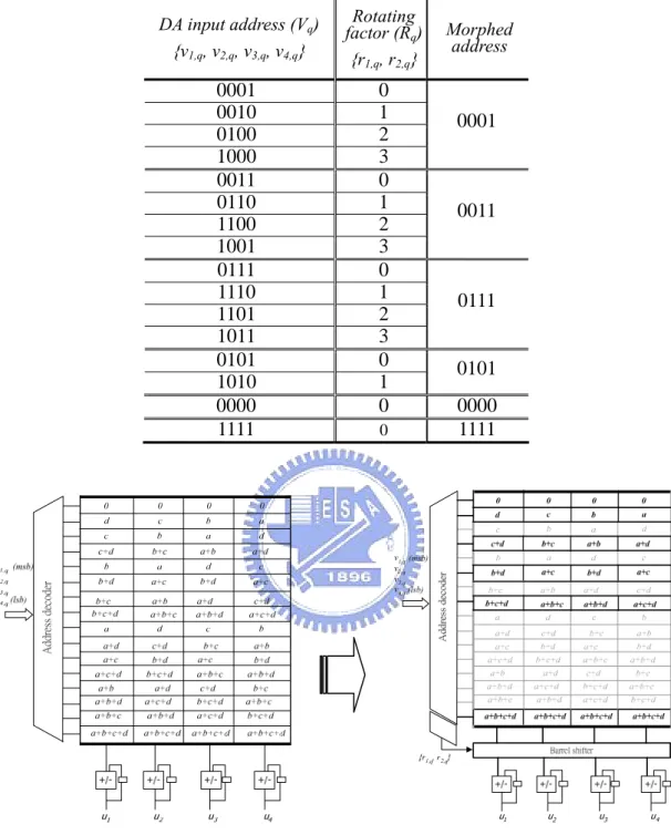
2.3.2 Address morphing approach
With the GDA design approach, the distribution of DA input address is reduced into few groups. Shown as Table 2.4, we can realize the cyclic convolution by using the scheme of address morphing that converts the distribution of DA input address into a subset of it with minimal transition activity such that the transition activity on the word lines of memory is reduced. Even in the case of never removing the unused entries of memory, due to the lower input activity, the power consumption of memory shown in Fig. 2.9 is reduced. Actually due to the number of memory entry is reduced in Fig. 2.9; the bit-line loading of memory and transition activity on the bit-lines are also reduced. Thus the power consumption of memory in the GDA design is reduced significantly. However, the barrel shifter in the overhead of GDA design consumes extra power such that the overall power consumption of GDA design with short length is improved inconspicuously.
Table 2.4: The relation ship of the address morphing. DA input address (Vq) {v1,q, v2,q, v3,q, v4,q} Rotating factor (Rq) {r1,q, r2,q} Morphed address 0001 0 0010 1 0100 2 1000 3 0001 0011 0 0110 1 1100 2 1001 3 0011 0111 0 1110 1 1101 2 1011 3 0111 0101 0 1010 1 0101 0000 0 0000 1111 0 1111
Fig. 2.9: The description of architecture transformation from DA to GDA
2.3.3 Exploration of dynamic range of the input data
The power consumption of a circuit highly depends on the transition activity of input data. In some video codec systems, the data to be processed is the difference of the adjacent frames such as the inter frame used in the video codec standards of
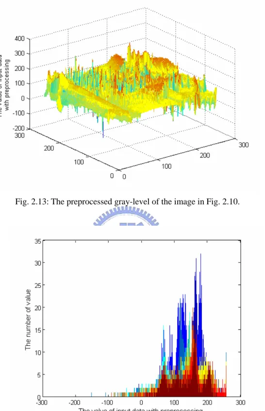
MPEG-2, MPEG-4, H.26X, and etc. As most of the pixels in the inter frame, the difference is with smaller value such that some of the higher bit in DA computation can be omitted to achieve lower power consumption. On the second concept, with the choice of DSP algorithm, sometimes the data fed into the processing unit needs to be processed previously such as the difference of input data. It means that we can exploit the property of correlation for the local data such that the dynamic range of these being processed data is reduced significantly. For example of 7-point DCT in cyclic convolution formulation, the data on the input of processing unit is not the direct input data. These data need to be computed previously with the combination of subtractions and additions. Fig. 2.10, Fig. 2.11, and Fig. 2.12 show the test image, gray-level of the pixels in this image, and histogram of the gray-level distribution, respectively. Fig. 2.13 and Fig. 2.14 respectively show the preprocessed gray-level and the histogram of the input data of processing unit in DCT design. It reveals that most of the preprocessed data values is small than the original one. Thus, the dynamic range is reduced for most of the input data. Combined with the second concept above, the number of cycle of DA computation in the DCT design will be reduced to achieve lower power consumption.
Fig. 2.11: gray-level of the pixels in the image of Fig. 2.10.
Fig. 2.13: The preprocessed gray-level of the image in Fig. 2.10.
Fig. 2.14: Histogram of the preprocessed data used in the example of 7-point DCT design.
2.3.4 Low Power Design with pre-computation scheme
Exploiting the property of spatial correlation in natural images, for the algorithm with the inputs formed as sum and difference of the primary inputs, the sum of inputs are likely to have a number of equal high-order bits, and the difference inputs are likely to have small dynamic range. Then for some cases, such as the 8-point 1-D DCT, the cycles of DA computation for the high-order bits of sum inputs can be skipped. On the other hand, since most of the bits in high-order bits of the difference of inputs are the sign-extension bits, with the manner of bit-serial and word-parallel, the cycles in DA computation for these extended sign-bits can also be skipped to achieve lower computation power [45]. In the following, we will illustrate the high-order bits rejection technique briefly, where this technique named most significant bit rejection (MSBR) in [45], and explore the distribution of pre-computed input data for the cyclic convolution formulation of prime-length DCT. For the realization of prime-length DCT, combining the proposed GDA design with the MSBR technique facilitates not only reducing the memory size, but also improving the power consumption.
MSBR technique
Considering the even and odd outputs of the reformulated 8-point 1-D DCT as
= 4 3 5 2 6 1 7 0 6 4 2 0 ⎥ ⎥ ⎥ ⎥ ⎥ ⎦ ⎤ ⎢ ⎢ ⎢ ⎢ ⎢ ⎣ ⎡ + + + + ⋅ ⎥ ⎥ ⎥ ⎥ ⎦ ⎤ ⎢ ⎢ ⎢ ⎢ ⎣ ⎡ − − − − − − ⎥ ⎥ ⎥ ⎥ ⎥ ⎦ ⎤ ⎢ ⎢ ⎢ ⎢ ⎢ ⎣ ⎡ x x x x x x x x C B B C A A A A B C C B A A A A X X X X , (2.4) = 4 3 5 2 6 1 7 0 1 5 3 1 ⎥ ⎥ ⎥ ⎥ ⎥ ⎦ ⎤ ⎢ ⎢ ⎢ ⎢ ⎢ ⎣ ⎡ − − − − ⋅ ⎥ ⎥ ⎥ ⎥ ⎦ ⎤ ⎢ ⎢ ⎢ ⎢ ⎣ ⎡ − − − − − − ⎥ ⎥ ⎥ ⎥ ⎥ ⎦ ⎤ ⎢ ⎢ ⎢ ⎢ ⎢ ⎣ ⎡ x x x x x x x x D E F G E G D F F D G E G F E D X X X X (2.5)
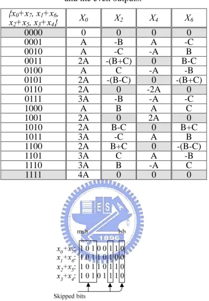
Observing the Table 2.5, we can see that some of candidates of DA input, i.e., 0000 and 1111, cause the even output to be zero. It means that the computation, shown as the rejected bits in Fig. 2.15, can be skipped in DA computation.
Table 2.5: Relationship between the sum of primary inputs and the even outputs.
{x0+x7, x1+x6, x2+x5, x3+x4} X0 X2 X4 X6 0000 0 0 0 0 0001 A -B A -C 0010 A -C -A B 0011 2A -(B+C) 0 B-C 0100 A C -A -B 0101 2A -(B-C) 0 -(B+C) 0110 2A 0 -2A 0 0111 3A -B -A -C 1000 A B A C 1001 2A 0 2A 0 1010 2A B-C 0 B+C 1011 3A -C A B 1100 2A B+C 0 -(B-C) 1101 3A C A -B 1110 3A B -A C 1111 4A 0 0 0
Fig. 2.15: The skipped bits in DA computation for the even outputs.
As for the computation of odd outputs, with the property of high spatial correlation for the pixels in an image, shown as Fig. 2.16 the difference of primary inputs reveals the property of small dynamic range, and thus most of the high-order bits in these difference inputs are the sign-extension bits. Then we need only computing for the least significant bit of sign-extension bits to have the exactly final result of DA computation. Similar to the sum inputs, the number of cycles in DA computation for these extended sign-bits can also be reduced significantly. However, due to the huge amount of overhead for skippable bits detection, development of the
efficient detection scheme is still the issue of low power GDA-based design with MSBR technique.
Fig. 2.16: The skipped bits in DA computation for the odd outputs.
Exploration of the input data for prime-length DCT in cyclic convolution
In the following, we illustrate how the MSBR technique can apply to the prime-length DCT design with the example of 7-point DCT. Considering the kernel of DCT T((3k)7) in (2.7), where x((3n-k+1)7 ) denotes the indirect inputs pre-computed
from the primary input y(n) as (2.8).
∑
= = 6 0 ) ( ) 0 ( n n y Y 6 ,...., 1 )); ) 3 ( ( cos( )] 0 ( ) ) 3 ( ( 2 [ ) ) 3 (( 7 14 7 7 = ⋅T +x ⋅ ⋅ k = Y k k π k (2.6) ) ) 3 ( cos( ) 1 ( ) ) 3 ( ( ) ) 3 ( ( 1 7 7 6 1 7 1 7 + = + − ⋅ − ⋅ ⋅ =∑
m n n k n k x T π (2.7)where (3k)7 denotes the result of “3k modulo 7” for short,
⎭ ⎬ ⎫ ⎩ ⎨ ⎧ < + − ≥ + − = +−−++ + − 0 1 ); ) 3 (( 0 1 ); ) 3 (( ) ) 3 (( 7 ) 1 ( 6 7 1 7 1 k n if x k n if x x n k k n k n
, the value of m is determined by
6 ,...., 1 , ; ) 3 ( ) 3 ( 7 ) 3
( n+1 7 +m⋅ = n−k+1 7 ⋅ k 7 n k= , and the sequence {x(n)} is defined
as