國 立 交 通 大 學
電子物理研究所
博 士 論 文
空間控制陣列結構中局域性表面電漿子之
研究
Studies on Localized Surface Plasmons in Spatially
Controlled Array Structures
研 究 生:周瑞雯
指 導 教 授:褚德三 博士
共同指導教授:周武清 博士
空間控制陣列結構中局域性表面電漿子之研究
博士生:周瑞雯 指導教授:褚德三 博士 共同指導教授:周武清 博士 國立交通大學 電子物理研究所 論 文 摘 要 本論文主要在探討具有空間控制的半導體陣列結構上,局域性表面電漿子(localized surface plasmons (LSPs))特性之研究。本論文的第一部份,我們以電子束刻版印刷
術(electron beam lithography (EBL))製作出三組不同間距的鍍金矽奈米柱樣品,然後以鎢燈
提供的白色光源照射該三組陣列結構,經由反射光譜的觀察,證實該三組陣列結構上 的局域性表面電漿子的共振頻率能被調變;鍍金矽奈米柱間距越大則表面電漿子共振 頻率越小(紅位移特性)。本論文的第一部份中,我們也探討了以二維有限元素法計算 模擬陣列近場範圍內的總能量分佈。近場模擬結果除了顯示局域性表面電漿子的分佈 情形和局域性表面電漿子頻率的紅位移特性外,還顯示陣列結構所特有的光柵特性- 也就是說,不同間距的結構(相當於光柵)都有對應能在其中形成建設性干涉的特定光 波長。在模擬分析中,由高階繞射項在近場範圍(包含角度範圍廣及高階繞射項所能 涵蓋的所有角度)內所形成建設性干涉可以被完全預測出來。然而,反射譜無法讓我 們觀察到上述的光柵效應,因為反射譜的觀察角度只有在入射角等於反射角的位置上 (此角度正好是零階繞射項)。) 在建立能提供在空間上排列整齊的局域性表面電漿頻率的陣列結構之後,我們進 行第二部份的研究,將量子點旋轉塗佈在蓋玻片上,再將三個不同間距的鍍金矽奈米 柱陣列結構先後分別置於已塗佈完成量子點的蓋玻片上。在三個陣列上,針對相同的
50顆目標量子點觀察其發光強度所受到的影響。我們發現在最密的陣列結構上量子點 與金奈米柱可能接觸的面積最大,因而量子點螢光強度減弱的比例最高。而最疏的結 構上,其局域性表面電漿子的頻率與量子點螢光頻率最接近,因而其螢光強度增強的 比例最高。另外,我們發展出一個新的技巧,使我們在測量量子點螢光強度時也能先 後取得陣列結構的光學影像(藉由移除濾鏡,將激發雷射光源聚焦在接近基版位置 處,得到基版位置明亮而柱子頂端黑暗的光學影像以定位陣列的位置)、量子點的螢 光影像(放回濾鏡,將激發雷射光源聚焦在量子點上),然後,將兩張影像疊加,進而 得以定出量子點與陣列的相對位置。藉由此項技巧,我們歸納出量子點在陣列樣品不 同相對位置上發光強度的變化規則。當量子點位在金柱表面所形成的局域性表面電漿 區域內或是位在兩金柱中點附近的建設性干涉區,螢光強度皆能增強。在螢光強度能 增強的兩個情形中,量子點位在金柱表面所形成的局域性表面電漿區域內,因為量子 點螢光能與局域性表面電漿子產生耦合效應, 使得量子點螢光具有較短的生命期。 而當量子點太靠近金柱(<10 nm)甚至接觸到金柱時,螢光強度減弱機會比較大。最 後,再由二維有限元素法,以電磁模型為基礎,在量子點螢光頻率條件下,計算總能 量在陣列結構近場空間中分佈的情形。我們得到與實驗一致的結果。
Studies on
Localized Surface Plasmons in Spatially
Controlled Array Structures
Student: Jui-Wen Chou Advisor: Prof. Der-San Chuu Co-Advisor: Prof. Wu-Ching Chou
Department of Electrophysics, National Chiao Tung University, Hsin-Chu, Taiwan, Republic of China
Abstract
This dissertation is devoted to study the localized surface plasmons (LSPs) in spatially controlled array structures. In the first part, three periodic Au coated Si nano rod (SiNR) arrays on Si substrate with different distances between the SiNRs were fabricated by electron beam lithography (EBL). The LSPs is induced when these spatially controlled array structures were irradiated by an un-polarized white light from a tungsten halogen lamp, we found that the trends of reflectance spectra indicate that the LSP frequency can be spatially controlled by manipulating the distances between the SiNRs of the arrays. In addition, the experimental results were compared with 2D numerical simulations based on the finite element method. The simulation result of each array in the near field regions can reveal subtle characteristic of the intensity distributions including the grating effects (the higher order diffractions) and more LSP modes than in the far field reflection observation.
After the investigation of the spatially controlled LSPs, we started the second part of the research, fluorescence signals of quantum dots (QDs) influenced by the three array
structures of the Au coated SiNRs. The QDs were spin-coated on a cover glass. And then, the three array structures were put upside down on the cover glass in sequence. We further developed a new technique which can obtain the optical image of the array structures without losing information of the QD locations at the time of QDs fluorescence measurement. We removed the filter and focused the excitation laser on the substrate to obtain the optical image of the array structures (the substrate is therefore bright, and the top of the SiNR is dark). And then, we put back the filter and focused the excitation laser on the QDs to obtain the fluorescence image of the QDs. After superposing the two images, the relative locations between the QDs and the Au coated SiNRs were defined. The same 50 QDs were successively observed on the three array structures (one by one). On the densest gold coated SiNRs array structure, the highest QDs fluorescence quenching rates are observed. And on the sparsest array structure which provides the LSP frequency closer to the emission band of QDs, the highest QDs fluorescence enhancement rates are observed. The QDs fluorescence enhancement effects are observed on the locations proximity enough (but not touched by the Au) to the Au coated SiNRs, and on the locations near the mid point of two Au coated SiNRs (where the constructive interference is formed). And we found again that when the QDs contact with Au coated SiNRs, instead of enhancement, a non-radiatve process may occur, leading to QDs fluorescence quenching. Finally, both in the near field region, 2D numerical simulation results are consistent with the experiment results.
Acknowledgments
感謝我的指導教授褚德三老師,一路上指引我研究的方向、給我很多鼓勵和支 持、給我最好的環境學習如何做研究。在這個過程中,很多時候,我忙了老半天完成 不堪一擊的東西,硬著頭皮想要趕著交差了事。老師總是嚴格看待,要我好好正視缺 點,想辦法改進。我很感謝老師的耐心指教,給我機會修正,否則我這個不算嚴以律 己的人,鐵定不可能進步太多。我還要感謝共同指導教授周武清老師,總是給我很多 的指導、建議和幫助。無論是與實驗相關的研究之道或是待人處世的道理,老師給的 都是最重要的提示。當然,我也要感謝實驗室的夥伴們,和我一起成長,有過許多失 敗,也完成一些不可能的任務。當然這些任務是因為有大家再三幫忙、一直互相加油 打氣,不然不可能的任務就真的還是不可能了! 特別感謝麥克博士、克莉斯汀教授和古舍立教授在實驗上和論文寫作上給我很多 的指點和幫忙。感謝我的好朋友們陪我度過抱怨很多或是坐立難安不然就是超級開心 的時刻。最後,我要感謝親愛的爸爸、媽咪、三姑、二姑、姊姊、妹妹,沒有你們的 愛心加持,我可能沒有勇氣開始這趟旅程也很有可能會半途而廢。Contents
Abstract in Chinese I
Abstract in English III
Acknowledgments V Contents VI List of Tables IX List of Figures IX Chapter 1 Introduction 1 1-1 Motivation 1 1-2 Surface Plasmons 2
Chapter 2 Experiments and Techniques 22
2-1 Micro Raman Spectrometer 22
2-2 Fluorescence Lifetime Imaging Microscopy 24
2-3 Scanning Near-Field Optical Microscope 27
2-4 Reflectance Spectrometer 29
Chapter 3 The Finite Element Method 31
Chapter 4 Fluorescence Signals of Core-shell Quantum Dots Enhanced by Single Crystalline Gold Caps on Silicon Nanowires 38
4-1 Introduction 38
4-2 Experiment 40
4-4 Discussion 50
4-5 Conclusion 57
Chapter 5 Observation of the Localized Surface Plasmons in Spatially Controlled Array Structures 62
5-1 Observed by Scanning Near-Field Optical Microscope 62
5-1-1 Introduction 63
5-1-2 Results 63
5-1-3 Conclusion 64
5-2 Observed by Reflectance Spectrometer 65
5-2-1 Introduction 65
5-2-2 Experiment 66
5-2-3 Results 68
5-2-4 Discussion 72
5-2-5 Conclusion 77
Chapter 6 Fluorescence Signals of Quantum Dots Influenced by Spatially Controlled Array Structures 80
6-1 Introduction 80
6-2 Experiment results and discussion 81
6-3 Conclusion 88
Chapter 7 Surface Enhanced Raman Scattering Observed on Spatially Controlled Array Structures 91
7-1 Introduction 93
7-2 Experiment results
94
7-3 Discussion 97
Chapter 8 Conclusion 106
Chapter 9 Future Works 109
List of Tables
Tab. 5.1: The peripheral distances and the diagonal distances, the incident wavelengths of the localized surface plasmons modes of array (a-c) observed in the reflectance spectra, 2D
finite element method simulations results…………..………...……..….71
List of Figures
Fig. 1.1: The characteristics of surface plasmons wave propagating at the interface of the metal-dielectric material...4Fig. 1.2: Surface plasmon polaritons excitation configurations……...………...6
Fig. 1.3: Three-channel microscope set-up reported by Lukin’s group………...9
Fig. 1.4: Optical Surface plasmons coupled to quantum dots with simulation results reported by Lukin’s group……...10
Fig. 1.5: Normalized energy flux for an emitter at different position……….11
Fig. 1.6: Nanoengineered fluorescent response of quantum dots……….….….12
Fig. 1.7: Reflectance spectra of quantum dot-doped samples for four different silver disk………...12
Fig. 2.1: Optical path simple description of the Micro-Raman spectrometer……….23
Fig. 2.2: Jobin Yvon LabRam HR800, side view I...………...…………..23
Fig. 2.3: Jobin Yvon LabRam HR800, side view II……..……….…...24
Fig. 2.4: The schematic diagram of fluorescence images and the lifetime measurement system………..26
Fig. 2.5: The fluorescence images and the lifetime measurement system...………26
Fig. 2.6: The scan near field optical microscope (SNOM)………...28
Fig. 2.7: The schematic of optical system of the reflectance spectrometer………...29
Fig. 3.1: Illustration of the eth segment and the linear shape functions………..…….34
Fig. 3.2: The computation domain and node coordinates for the eth triangle.…………...36
Fig. 4.1: SEM images of silicon nanowires grown by electron beam evaporation………..44
Fig. 4.2: TEM and SEM cross sectional micrograph of a silicon nanowire, and oblique SEM micrograph of silicon nanowires after chemical gold-cap removal……….45
Fig. 4.3: Fluorescence PL study of quantum dots on different substrates………....46
Fig. 4.4: Fluorescence PL measurements quantum dots on different locations on silicon nanowires with nanoscale gold-caps on silicon (111) substrates……….….47
Fig. 4.5: High resolution SEM micrographs that show the quantum dots on silicon nanowires with nanoscale gold-caps on silicon (111) substrates…...49
Fig. 4.6: Electron backscatter diffraction pattern of a gold-cap on a silicon nanowires ….50 Fig. 4.7: Finite element modeling of the electromagnetic field enhancement at a silicon nanowire with gold-cap atop………..…………...52
Fig. 4.8: Maximum enhancement factor deduced from 2D finite element method calculations……….……….………..……….53
Fig. 4.9: Fluorescence signals Time-Correlated Single Photon Counting analysis of single quantum dots on silicon nanowires with and without gold-cap………55
Fig. 5.1: SEM images of the array structure and the NSOM images of different incident wavelengths………..………..64
Fig. 5.2: Localized Surface Plasmons in Spatially Controlled Array Structures: SEM images, reflectance spectra and 2D finite element method simulation results...65
Fig. 5.3: SEM images of gold-coated silicon nanorods arrays, a unit cell of array, the mesh diagram, the integration areas, the enhancement factors calculated in the
integration areas of array (c)………..……...67
Fig. 5.4: Reflectance spectra of array (a-c)………..…………..………..70
Fig. 5.5: 2D finite element method calculations of the normalized time average total
energy densities of array (a-c)………...……….….73
Fig. 5.6: Reflectance spectra and 2D finite element method simulations results of array
(a-c)……….……….………...…....74
Fig. 6.1: SEM images of gold-coated silicon nanorods arrays, schematic view of the sample structure, and the reflectance spectra of arrays (a-c)……….…...82 Fig. 6.2: Fluorescence images of 50 different quantum dots on arrays, statistic event
numbers of the enhancement factors, the multi channel scalar and the Time-Correlated Single Photon Counting of one of the single quantum dots picked up from the 50 quantum dots on arrays and on the glass.……….84 Fig. 6.3: The quantum dots fluorescence images, the reflectance image combined with
schematic square unit cell, Time-Correlated Single Photon Counting and multi channel scalar trace and simulation results………...87 Fig. 7.1: SEM image of one of the gold nanoparticle array structures and the surface
enhancement Raman scattering results reported by N. Félidj et al………….…..92 Fig. 7.2: SEM images, optical images, and the Raman mapping of gold-coated silicon
nanorods arrays…….………..………..………...94
Fig. 7.3: Surface enhanced Raman scattering and average surface enhanced Raman
scattering of the molecule crystal violet aqueous on arrays………..……96 Fig. 7.4: Reflectance spectra of arrays………..………..……...98 Fig. 7.5: Finite element method analysis of arrays………...…………...100
Fig. 9.1: SEM images of AFM tip and the nanowire tip……..……..………..…..109 Fig. 9.2: Setup of the Tip Enhancement Raman Spectroscopy with Si nanowire tip
measurement……….………..………
…
110Fig. 9.3: Enhanced Raman spectra of malachite green……….……….………...111 Fig. 9.4: Electron micrograph of various metal structures..………..……
…
.....
112 Fig. 9.5: Light excites a surface plasmon resonance on a metal nanoparticle and is coupledinto silicon, simulation of increased light intensity beneath a metal nanoparticle on a silicon cell, and SEM image of silver nanoparticles on a solar cell……....113
Chapter 1 Introduction
§ 1-1 Motivation
Lukin’s group [1], has demonstrated a cavity-free, broadband approach for engineering photon-emitter (the CdSe quantum dots (QDs) [2]) interactions [3, 4] via sub-wavelength confinement of optical fields near metallic nano-structures (the silver nanowires) [5-8]. It should be interesting to investigate which geometric size and shape of metallic structures can be coupled to QDs and generate surface plasmons (SPs) [9-10] with frequencies we hope. Our research topics about the colloidal QDs fluorescence influenced by the localized surface plasmons (LSPs) [10-25] were investigated by two series of candidates, i.e. the substrate of gold-caps on top of Si nanowires (SiNWs) [26-27] (inhomogeneous in size and shape) and the substrate of gold-coated Si nanorod (SiNR) array structures [28-29] (homogeneous in size and shape). Gold was chosen for it is a good metal [30-31] for forming surface plasmon polaritons (SPPs) [32-48] on its surface. For the first series of substrate, by the gold-catalyzed vapour-liquid-solid (VLS) growth mechanism fabricated gold-caps on top of SiNWs [26-27, 49-51] which provided proper surface conditions for forming the LSPs resonance, we observed the fluorescence signal enhancement of the QDs [27] (illustrated in chapter 4). However, the gold-caps on top of SiNWs fabricated by the VLS growth mechanism (based on the addition of certain metal impurities and small globules of the impurity (not with regular sizes and shapes) are located at the tip of the wire during growth [52-53]) are not with regular sizes and shapes. Since the LSPs resonance frequencies are strongly dependent on the geometric sizes and shapes of the metallic particles, there are difficulties in analyzing how the fluorescence is influenced.
Hence, the second series of substrates were fabricated, by electron beam lithography (EBL) properly arranging the geometric configurations of gold-coated SiNR array structures, we are able to manipulate the LSPs resonance frequencies [28-29]. The geometries of the array structures were designed based on the finite element method (FEM) [54-55] (will be illustrated in chapter 3) which can obtain the near-field distribution of the array structures for estimating the target LSPs resonance frequencies. By the proper design of the distances between the SiNRs of array structures, we can spatially control the LSPs resonance frequencies. The relative LSPs topics investigated by the second series of substrate “gold-coated SiNR array structures” (which is corresponding to the title of the dissertation) will be illustrated in chapter 5, 6 and 7 [28-29].
§ 1-2 Surface plasmon
After a brief illustration of the motivation and the arrangement in the dissertation, we would like to give an introduction to the SPs [9-10] in the following. SPs were first brought up by Ritchie in the 1950s [10], and were extensively studied in the following two decades. The relative applications are getting hotter in the modern age due to the progress of the nanometer-sized structure manufacture technology. Many possible applications such as the surface enhanced Raman scattering (SERS) [56-64], solar cells [65], plasmon waveguides [66], filters and microscopy [67-68], etc. have been developed and improved till now.
SPs [9-10] are coherent electron oscillations at the interface between any two materials with opposite sign of the dielectric function (in the real part) across the interface (for example: the matel-dielectric interface, the metal-air interface). When SPs [9-10] couple with a photon, the resulting hybridised excitation is called a surface plasmon polariton
(SPP) [32-48]. In other words, a combined excitation consisting of a surface plasmon and a photon is called a SPP [68-71]. The light waves are trapped on the metal surface due to their interaction with the free electrons (provided by the metal). And the free electrons which are in resonance with the light wave oscillate collectively. At the moment, the SPPs [68-71] are formed. In addition to SPs [9-10] on a plane surface, excitations of electron plasmons bounded in geometries such as bumps or voids are called LSPs [10-25, 68, 72]. It is worthwhile to mention that the SPP mode can be excited only if both the frequency and wave vector of the excitation light match the SPP frequency and the SPP wave vector; where as the LSP mode can be resonantly excited with light of appropriate frequency with arbitrary excitation light wave vector [68]. LSP resonances play an important role when the SPPs propagate on rough surfaces. Significant enhancement due to the SPP scattering can be found on surface defects when the frequency of SPP and resonant frequency of LSP are close to each other [66, 73-75].
For the interface of the metal and the dielectric infinite plane, Eq. (1.1) describes the relation between the frequency-dependent SP wave vector and the frequency-dependent electromagnetic wave vector in the free space.
sp k 0 k m d m d sp k k ε ε ε ε + = 0 (1.1) Where εm and εd is the frequency-dependent permittivity of the metal and the dielectric material respectively. For the interface of the metal-dielectric, >1
+ m d m d ε ε ε ε , the momentum of the SP mode hksp is greater than that (hk0) of a free-space photon [68].
When the SPs wave propagating at the interface of the metal-dielectric material, the transverse magnetic (parallel to the interface) and the electric field (normal to the interface) are formed as shown in Fig. 1.1(a). This character based on the electromagnetic theory leads to the field enhancement near the surface and decaying exponentially with distance
away from the metal surface as shown in Fig. 1.1(b). The field decaying away from the surface is corresponding to the field bounded near the surface which leads to the non-radiative feature of SPs (preventing power from propagating away from the surface) [12].
Figs. 1.1(a)(b)(c) The characteristics of SPs wave propagating at the interface of the
metal-dielectric material [12]
Eq. (1.1) can be obtained by solving the Maxwell’s equations [55] with continuous boundary conditions on the interface. The full set of Maxwell’s equations in the absence of external sources can be expressed as follows:
i i1 i, t c E H ∂ ∂ = × ∇ ε (1.2) i 1 i, t c H E ∂ ∂ − = × ∇ (1.3) ∇⋅(εi E i)=0, (1.4) ∇⋅ H i =0, (1.5) For the interface shown in Fig. 1.1(a), the index can be applied for the dielectric or for the metal, i.e. i=d or i=m. Solutions of equations (1.2)-(1.5) can be expressed as:
i , ) , 0 , ( z i(kx t) iz ix i i i e e E E −κ −ω = E (1.6)
, ) 0 , , 0 ( z i(kx t) iy i i i e e H −κ −ω = H (1.7) Where and are for the x and z component electric fields respectively, and is for the y component magnetic field. is the frequency-dependent electromagnetic wave vector, and
ix
E Eiz Hiy
i
k
ω is the angular frequency. 2
2 2 c ki i i ω ε
κ = − , the exponential term with negative real argument e−κiz is corresponding to the feature of z component field
e m
the decay length of the field [12] is defined as
bounded near the surface of th etal, as shown in Fig. 1.2(b). Above the metal surface,
d
d κ
δ = 1 , i.e. when the filed falls to 1/e, and is in the order of half wavelength of involved light whereas inside the metal, the decay length is determined by the skin depth [12]
m
m κ
δ = 1 .
Substitute Eq. (1.6) and Eq. (1.7) into Eqs. (1.2)-(1.5) with the boundary condition that the electric and m
wave vector and the wave vector in the free space. The dispersion relation is shown in Fig. 1.1(c). For the same angular frequencies, the SP modes have higher
the dielectric and the metal can be solved analytically, however, for the othe
agnetic fields parallel to the interface of the dielectric material and the metal must be continuous, one obtains Eq. (1.1) to describe the relation between the SP
momentum than the light in the free space [12].
Although the SPPs in the infinite plane interface between
sp
k k0
r complicated cases such as our gold-caps on SiNWs substrates and gold-coated SiNR array structures, the analytic solutions are not available. When the geometry of the interface is complicated, and the problem cannot be solved analytically, the FEM [54-55] provides reliable numerical solutions and is usually applicable. Therefore, we use the FEM to design our array structures and analyze the LSP problems for our array structures.
By the way, from the SPP dispersion relations (Eq. 1.1), we found that the SPP wave vector ( ) is larger than the photon wave vector ( ) which means that the light illuminating a plane surface cannot be directly coupled to surface polaritons [
sp
k k0
20, 68]. Special experimental arrangements by Kretschmann [76] and Otto [77] as shown in Figs. 1.2(a-c) have been designed to provide the condition for matching the wave vector of the photon and the SPP. In the Kretschmann’s setup [68, 76] (Fig. 1.2(a)), light incidents to the metal film through the dielectric prism at an angle of incidence greater than the angle of total internal reflection [76]. At a certain angle of incidence θ where the in-plane
component of the photon wave vector in the prism coincides with the SPP wave vector on an air–metal surface, resonant light tunneling through the metal film occurs and light is coupled to the surface polaritons [68]:
θ ε
ω prismsin
sp c
k = . (1.8)
Figs. 1.2 SPP excitation configurations: (a) Kretschmann geometry, (b) two-layer
Kretschmann geometry, (c) Otto geometry. [68]
Under these resonant conditions, because light is coupled to SPPs with high efficiency, a sharp minimum reflectivity is observed from the prism interface [68]. When increase the thickness of the metal film, the efficiency of the SPP excitation decreases (because the tunneling distance is increased). SPP on an interface between the prism and metal cannot be excited anymore when the wave vector of SPP at the interface is greater than the photon
wave vector in the prism (at all possible incident angles). An additional dielectric layer (with a refractive index smaller than the refraction index of the prism) should be deposited between the prism and the metal film (Fig.1.2 (b)). In such a setup, the photon tunneling through this additional dielectric layer can provide resonant excitation of SPP on the inner interface.
For thick metal films (or surfaces of bulk metal), SPP can be excited in the Otto’s setup [68, 77] (as shown in Fig. 1.2(c)). In the setup, similar to Kretschmann’s setup (Fig. 1.2(b)), the additional dielectric layer is the air. The prism where total internal reflection occurs is placed close to the metal surface, so that photon tunneling occurs through the air gap between the prism and the surface [68, 77]. And of course, the resonant conditions can also be derived from (Eq. (1.8)).
In the Following, we give an illustration of the colloidal QDs which contain wide applications and play an important role in our research. A quantum dot (QD) is a semiconductor whose excitons are confined in three dimensions [78-80]. The chemical colloidal synthesis is one of several different methods (such as lithographic techniques, epitaxial techniques by chemical methods, ion implantation) to fabricate QDs. Many different chemical compositions of colloidal QDs can be possibly synthesized, for examples, cadmium selenide (CdSe), cadmium selenide tellurium (CdSeTe), cadmium sulfide (CdS), indium arsenide (InAs), and indium phosphide (InP), etc. The diameters of the colloidal QDs are ~ 2 to 10 nm which possibly contain 100~ 100000 atoms [81].
Colloidal QDs are synthesized based on a three-component reaction medium, i.e. precursors, organic surfactants, and solvents. By heating the reaction medium to a sufficiently high temperature, the precursors can be chemically transformed into monomers. When the monomers reach a high enough supersaturating level, the nanocrystal growth starts with a nucleation process. The temperature and the monomer concentration are two critical factors in determining optical conditions of the colloidal QDs [81]. For excellent
condition controlling, the QDs fluorescence photo luminescence signals exhibit narrow and symmetric emission peaks (FWHM typically in the few 10 nm range) [80-84].
Two important optical features of the QDs are the tuneable fluorescence frequencies and the quantized energy spectra with quantized density of states near the band gap edges. Due to quantum confinement which causes the band gap energy varying with the particle size [78-81, 85-91], by tuning the chemical composition and the particle size of QD, fluorescence emission wavelength of the QD varied in a wide range, from 400 to 2000 nm. The band gap energy which determines the fluorescence energy of the QD is inversely proportional to the square of the size of the QD [81]. The larger the QD size, the lower frequency of its fluorescence spectrum.
Till now, comprehensive QD applications in optoelectronics devices such as solar cells [92], light-emitting diode (LEDs) [93], and diode lasers [94], biological and medical studies (investigated QDs as agents for medical imaging [95]), and quantum computation [95-96] have been carried out. In modern biological analysis, QDs are superior to traditional organic dyes on brightness (due to 20 times higher quantum yield) and stability (due to less photobleaching) [81, 84, 97-106]. The QDs applications are widely developed in the study of intracellular process at the single molecule level, high-resolution cellular imaginglong-term in vivo observation of cell trafficking, tumour targeting, and diagnostics [107-109] etc.
QDs can be synthesized with larger (and thicker) shells and formed core/shell structures. In this study (will be illustrated in chapter 4 and 6) we choose the commercial core/shell CdSeTe/ZnS [2] colloidal QDs in a highly dilute aqueous solution, the wavelength of the fluorescence center is at 705 nm.
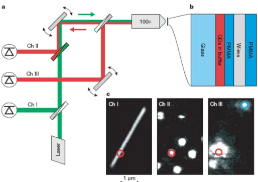
Fig. 1.3 Experimental set-up a, Three-channel confocal microscope with 532 laser excitation source. b, Layout of sample containing QDs and Ag NWs. The samples were created by spinning QDs onto a glass substrate, covering them with ~ 30nm layer of poly (methylmethacrylate), and then depositing dry wires on top. Finally, the sample was overcoated with a thick layer of PMMA. c, Left, channel I: Ag NW image. Middle, channel II: image of QDs. The red circle denotes the position of the coupled QD, and the same point is also denoted in the leftmost image. Right, channel III: the excitation laser was focused on the QD (red circle). The largest bright spot corresponds to the QD fluorescence, while two smaller spots correspond to SPs scattered from the Ag NW ends. The blue circle indicates the farthest end of the NW, used for photon cross-correlation measurements. [1]
After reviewing the previous experimental arrangements of SPs and the illustration of colloidal QDs [2], now let us review two previous relative papers in the following. In the year of 2007, M. D. Lukin et al. reported that the observation of single optical plasmon in silver nanowires (Ag NWs) coupled to the CdSe single quantum dot (SQD) as shown in Fig. 1.3c by the three-channel set-up (the excitation source: 532 nm wavelength laser, power <4μW ) as shown in Figs. 1.3a-b, When a SQD is excited in close to an Ag NW, fluorescence occurs from the SQD coupled to SPs in the Ag NW. At the moment, not only the SQD fluorescence (more than 2.5-fold enhancement) is emitted but also two end sides of the wire are lightened up (due to couple to SPs) as shown in Fig. 1.3c.CHIII.
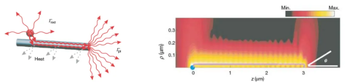
Fig. 1.4 Radiative coupling of QDs to conducting nanowires (NWs). In the left side, a
coupled QD can either spontaneously emit into free space or into the guided SPs of the NW with respective rates . In the right side, simulations of the electric field amplitude (arbitrary units) emitted by a dipole (blue filled circle) positioned 25 nm from one end of a conducting NW (whose surface is outlined)
pl rad Γ Γ ,
m
μ
3 in length and 50 nm in diameter. The vertical scale (ρ ) is enlarged compared to the horizontal ( z ) to clearly show the near field of the SP energy is clearly scattered into the far-field, while the remaining is either lost to dissipation or to back-reflection. θ is the emission angle. [1]
Similar to the optical modes of a conventional dielectric fiber, a broad continuum of SP modes can be confined on a cylindrical metallic wire and guided along the wire axis [7-8] as shown in Fig. 1.4 (the left side). The field confinement with reduced velocity of SPs which occurs when the QD fluorescence coupled into the guided SP modes [4] is much like a lens with extraordinarily high numerical aperture. For an optimally placed emitter, the spontaneous emission rate into SPs is larger than the radiative ( ) rate and
non-radiative rate ( ), which results in highly efficient coupling to SPs and enhancement of the total decay rate (
pl
Γ Γrad
nrd Γ
total
Γ ) compared to that of an uncoupled emitter (Γ ). 0 This enhancement can be characterized by a Purcell factor, P=Γtotal/Γ0 [1, 4]. A
simulation of the SPs in this case is shown in Fig. 1.4 (the right side). A QD is placed 25 nm away from one of the Ag NW’s end (marked with the blue circle). The SPs decay from the edge of Ag NW. The fluorescence from the QD emits into free space, and the SP scattering appears at the other end of the Ag NW.
Normalized energy flux of the typical position for an emitter is demonstrated by the FEM simulation (combined with coupled-mode theory) as shown in Figs. 1.5(a-c) [110]. In Fig. 1.5(a), the emitter is at the distance k0d =0.002 (very close to the nanotip): the emitter decays primarily nonradiatively. In Fig. 1.5(b), the emitter is at the distance : efficient excitation of guided plasmons. And in Fig. 1.5(c), the emitter is at the distance : associated with radiative decay.
2 . 0 0d = k 7 . 0 0d = k
Figs. 1.5Normalized energy flux for an emitter (denoted by the blue circle) positioned at the distance (a)k0d =0.002, (b)k0d =0.2 and (c)k0d =0.7 from the nanotip. The surface of the nanotip is indicated by the dotted lines. [110]
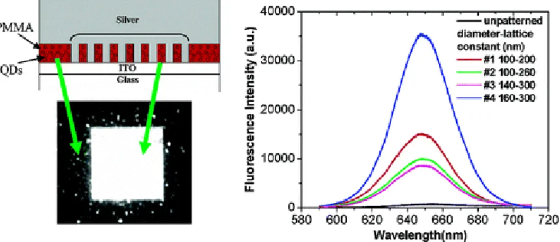
Another paper closely related to our work was reported by Arto V. Nurmikko et al. In 2005, [70], this article reported that the fluorescent from QDs in proximity to the SPP field of periodic Ag nanoparticle arrays can be enhanced. Tuning the SPP resonances to the QD exciton emission band results in an enhancement of up to ~ 50- fold in the overall fluorescence efficiency as shown in Fig. 1.6. Propagating modes of SP resonances can be tuned by varying the diameters and the lattice constants of the Ag nanoparticle arrays. As shown in Fig. 1.7, the valley in the reflectance spectra which corresponding to the LSP can
be tuned by different diameters and lattice constants of the Ag nanoparticle arrays. The larger the diameter (and the lattice constant), the lower the LSP frequency.
Fig.1.6Nanoengineered fluorescent response is reported from semiconductor core−shell (CdSe/ZnS) QDs in proximity to the SPP field of periodic Ag nanoparticle arrays (as shown in the left upper side). Propagating modes of SP resonances have a direct impact on the fluorescence enhancement (as shown in the left lower side and the PL in the right side) [70].
Fig. 1.7 Normal incident reflectance spectra of QD-doped samples for four different Ag disk diameters and lattice constants labeled from #1 through #4. Respective diameter and lattice constants are as follows: #1, 100 and 200 nm; #2, 100 and 260 nm; #3, 140 and 300 nm; #4, 160 and 300 nm [70].
Comparing with our results, by two series of substrates “Au caps on top of SiNWs” (will be illustrated in chapter 4) and “Au coated SiNR array structures” (will be illustrated in
chapter 5 and 6), we investigated the LSP and how the QDs fluorescence can be influenced. On both series of substrates, we observed QDs fluorescence enhancement on hot spots (the hot spots are specific regions (near the metal surface) where the high electromagnetic fields (caused by LSP coupling) are formed) [27-29]. However, the first series of substrate “Au caps on SiNWs” is inhomogeneous in size and shape and the number of the hot spots is rare (not so efficient for enhancement), we started to design the second series of substrate “Au coated SiNR array structures” [28-29] based on 2D FEM [54-55]. We found that by tuning the distance between the SiNRs of the array structures, we can spatially control the LSP resonance modes [28]. And since arrays of the hot spots were formed by this way, much more efficient enhancement can be reached [29] (chapter 5 and 7). By developing a new technique which obtains the optical image of the array structures without losing information of the QD locations, we are able to further investigate how the QDs fluorescence influenced by spatially controlled array structures [29]. We found QDs fluorescence on the array structures can be enhanced or quenched (depend on the relative positions between the QDs and the Au coated SiNRs) [29, 101], and 2D FEM [54-55] simulation results are helpful for analyzing the experiment results [27-29].
Reference:
[1] Akimov A. V., Mukherjee A., Yu C. L., Chang D. E., Zibrov A. S., Hemmer P. R., Park H. & Lukin M. D. Nature 450, 402(2007)
[2] http://tools.invitrogen.com
[3] Chang D. E, Sørensen A. S., Demler E. A. and Lukin M. D. A Nature Phys. 3, 807
[4] Chang D. E, Sørensen A. S., Hemmer P.R. and Lukin M. D. Phys. Rev. Lett. 97, 053002
(2006)
[5] Atwater H. A. Sci. Am. 296, 56 (2007)
[6] Genet C. and Ebbesen T. W. Nature 445, 39(2007)
[7] Sanders A. W. et al. Nano Lett. 6, 1822(2006)
[8] Ditlbacher Harald, Hohenau Andreas, Wagner Dieter, Kreibig Uwe, Rogers Michael, Hofer Ferdinand, Aussenegg Franz R., and Krenn Joachim R. Phys. Rev. Lett. 95, 257403(2005)
[9] Raether H, Surface Plasmons, Berlin, Springer (1988) [10] Ritchie R. H. Phys. Rev. 106, 874 (1957)
[11] Stern E. A. and Ferrell R. A. Phys. Rev. 120, 130 (1960)
[12] Barnes William L., Dereux Alain, and Ebbesen Thomas W. Nature 424, 824 (2003)
[13] Boardman A D ed. Electromagnetic Surface Modes, New York, Wiley (1982)
[14] Kreibig U and Vollmer M Optical Properties of Metal Clusters, Berlin, Springer
(1995)
[15] Shchegrov A V, Novikov I V and Maradudin A A Phys. Rev. Lett. 78 4269(1997)
[16] Xiao M, Zayats A V and Siqueiros J Phys. Rev. B 55 1824(1997)
[17] Moskovits M Rev. Mod. Phys. 57 783(1985)
[18] Ponath H-E and Stegeman G I (eds.) Nonlinear Surface Electromagnetic Phenomena,
[19] Shalaev V M Nonlinear Optics of Random Media, Berlin, Springer (2000)
[20] Ushioda S, Uehara Y and Kuwahara M Appl. Surf. Sci. 60 448(1992)
[21] Smolyaninov I, Zayats A and Davis C Phys. Rev. B 56 9290(1997)
[22] Zayats A V and Sandoghdar V Opt. Commun. 178 245(2000)
[23] Malshukov A G Phys. Rep. 194 343(1990)
[24] Zayats A V Opt. Commun. 161 156(1999)
[25] Mills D L Phys. Rev. B 65 125419(2002)
[26] Becker M. , Sivakov V., Andrä G., Geiger R., Schreiber J., Hoffmann S., Michler J., Milenin A. P., Werner P., and Christiansen S. H. Nano Letters 7, 75(2007)
[27] Christiansen S H, Chou J W, Becker M, Sivakov V, Ehrhold K, Berger A, Chou W C, Chuu D S, Gösele U Nanotechnology 20, 165301 (2009)
[28] Chou J W, Lin K C, Lee Y J, Yuan C T, Hsueh F K, Shih H C, Fan W C, Luo C W, Lin M C, Chou W C, Chuu D S Nanotechnology 20, 305202 (2009)
[29] Chou J W, Lin K. C. , Tang Y. T., Lee Yao-Jen, Luo C.W., Chen Y. N, Yuan C. T., Shih Hsun-Chuan, Lin M. C. , Chou W. C. , Chuu D. S. Nanotechnology 20, 415201
(2009)
[30] Joannopoulus J D, Meade R D and Winn J N Photonic Crystals, Princeton, NJ:
Princeton University Press (1995)
[31] Agranovich V M and Mills D L (eds.) Surface Polaritons, Amsterdam, North-Holland
(1982)
[33] Courjon D, Sarayeddine K and Spajer M Opt. Commun. 71 23(1989)
[34] Fornel F. de , Goudonnet J P, Salomon L and Lesniewska E Proc. SPIE 1139 77
(1989)
[35] Marti O, Bielefeldt H, Hecht B, Herminhaus S, Leiderer P and Mlynek J Opt. Commun. 96 225(1993)
[36] Adam P M, Salomon L, de Fornel F and Goudonnet J P Phys. Rev. B 48 2680(1993)
[37] Dawson P, de Fornel F and Goudonnet J P Phys. Rev. Lett. 72 2927(1994)
[38] Tsai D P, Kovasc J, Wang Z, MoskovitsM, Shalaev V M, Suh J S and Botet R Phys. Rev. Lett. 72 4149 (1994)
[39] Bozhevolnyi S I, Smolyaninov I I and Zayats A V Phys. Rev. B 51 17916 (1995)
[40] Bozhevolnyi S I, Vohnsen B, Smolyaninov I I and Zayats A V Opt. Commun. 117 417
(1995)
[41] Bozhevolnyi S I, Vohnsen B and Zayats A V Optics at the Nanometer Scale ed M
Nieto-Vesperinas and N Garcia, Dordrecht, Kluwer Academic, p 163 (1996)
[42] Hecht B, Bielefeldt H, Novotny L, Inouye Y and Pohl D W Phys. Rev. Lett. 77 1889
(1996)
[43] Laks B, Mills D L and Maradudin A A Phys. Rev. B 23 4965 (1981)
[44] Glass N E, Weber M and Mills D L Phys. Rev. B 29 6548 (1984)
[45] Barnes W L, Preist T W, Kitson S C and Sambles J R Phys. Rev. B 54 6227 (1996)
[47] Bozhevolnyi S I, Erland J, Leosson K, Skovgaard P M W and Hvam J M Phys. Rev. Lett. 86 3008 (2001)
[48] Smolyaninov I I, Zayats A V, Stanishevsky A and Davis C C Phys. Rev. B 66 205414
(2002)
[49] Sivakov V., Andrä G., Gösele U., and Christiansen S. phys. stat. sol. (a) 203, 15, 3692
(2006)
[50] Sivakov V., Andrä G., Himcinschi C., Gösele U., Zahn D. R. T., Christiansen S. Appl. Phys. A 85, 311 (2006)
[51] Vladimir Sivakov, Frank Heyroth, Fritz Falk, Gudrun Andrä, Silke Christiansen
Journal of Crystal Growth 300, 288(2007)
[52] Wagner R.S., Ellis W.C. Appl. Phys. Lett. 4, 89 (1964)
[53] Schmidt Volker, Wittemann Joerg V., Senz Stephan, and Gösele Ulrich Ade. Mater.
21, 2681 (2009)
[54] Jin Jianming, The Finite Element Method in Electromagnetics, Second Edition, JOHN
WILEY & SONS. INC. (2002)
[55] Volakis John L., Chatterjee Arindam, Kempel Leo C., Finite Element Method for Electromagnetics-antennas, microwave circuits, and scattering applications, IEEE
PRESS (1998)
[56] Félidj N., Aubard J., Lévi G. Phys. Rev. B 65, 075419 (2002)
[57] Ibach Harald and Lüth Han, Solid-State Physics ―An Introduction to Principles of Materials Science, Second Edition, Springer (2002)
[58] Christiansen S. H., Becker M., Fahlbusch S., Michler J., Sivakov V., Andrae G., and Geiger R. Nanotechnology 18, 035503 (2007)
[59] Becker M., Sivakov V., Goesele U., Stelzner T., Andra G., Reich H. J., Hoffmann S., Michler J., and Christiansen S. H. Small 4, 398 (2008)
[60] Wang Y., Becker M., Wang L., Liu J., Scholz R., Peng J., Gösele U., Christiansen S., Kim D. H., Steinhart M. Nano Lett. 9, 2384 (2009)
[61] Tsang J. C., Kirtley J. R. and Bradley J. A. Phys. Rev. Lett. 43, 772 (1979)
[62] Lyon S. A. and Worlock J. M. Phys. Rev. Lett. 51, 593 (1983)
[63] Murray C. A., Allara D. L. and Rhinewine M. Phys. Rev. Lett. 46, 57 (1981)
[64] Nie Shuming and Emory Steven R. Science 275, 1102 (1997)
[65] Service Robert F. Science 319, 718 (2008)
[66] Maier Stefan A., Kik Pieter G., Atwater Harry A., Meltzer Sheffer, Harel Elad, Koel Bruce E., and Requicha Aria G. Nature Material 2, 229 (2003)
[67] Flätgen Georg, Krischer Katharina, Pettinger Bruno, Doblhofer Karl, Junkes Heinz, and Ertl Gerhard Science 269, 668 (1995)
[68] Zayats Anataly V and Smolyaninov Igor I. J. Opt. A: Pure Appl. Opt. 5, S16 (2003)
[69] Pitarke J. M., Silkin V. M., Chulkov E. V. and Echenique P. M. Rep. Prog. Phys. 70, 1–87 (2007)
[70] Song Jung-Hoon, Atay Tolga, Shi Sufei, Urabe Hayato, and Nurmikko Arto V. Nano Lett. 5, 1557 (2005)
[71] Kneipp Kartrin, Moskovits Martin, and Kneipp Harald: Surface-Enhanced Raman Scattering, Springer (2006)
[72] Chuang Wen-Hung, Wang Jyh-Yang, Yang C. C. and Kiang Yean-Woei Appl. Phys. Lett. 92, 133115 (2008)
[73] Shchegrov A V, Novikov I V and Maradudin A A Phys. Rev. Lett. 78 4269 (1997)
[74] Xiao M, Zayats A V and Siqueiros J Phys. Rev. B 55 1824 (1997)
[75] Agranovich V M, Kravtsov V E and Leskova T A Solid State Commun. 47 925 (1983)
[76] Kretschmann E and Raether H Z. Naturf. A 23 2135 (1968)
[77] Otto A Z. Phys. 216 398 (1968)
[78] Efros A.L. Sov. Phys. Semicond. 16, 772 (1982)
[79] Ekimov A.I. and Onushchenko A.A. Sov. Phys. Semicond. 16, 775 (1982)
[80] Alivisatos A.P. J. Phys. Chem. 100, 13226 (1996)
[81] http://en.wikipedia.org/wiki/Quantum_dot
[82] Alivisatos A.P. Science 271, 933 (1996)
[83] Bruchez Jr. M., Moronne M., Gin P., Weiss S. and Alivisatos A.P. Science 281, 2013
(1998)
[84] Chan W.C.W., Nie S. Science 281, 2016 (1998)
[85] Qu L.H. and Peng X.G. J. Am. Chem. Soc. 124, 2049 (2002)
[86] Zhong X.H., Feng Y.Y., Knoll W. and Han M.Y. J. Am. Chem.Soc. 125, 13559 (2003)
[88] Kim S., Fisher B., Eisler H.J. and Bawendi M. J. Am. Chem.Soc. 125, 11466 (2003)
[89] Wehrenberg B.L., Wang C.J. and Guyot-Sionnest P. J. Phys. Chem. B 106, 10634
(2002)
[90] Silbey Robert J., lberty Robert A. and Bawendi Moungi G., Physical Chemistry,
4thEdition, John Wiley &Sons, Page 835 (2005)
[91] C. Pollock, Fundamentals of Optoelectronics, Irwin, Boston, MA (1995)
[92] Huynh Wendy U., Dittmer Janke J. and Alivisatos A. Paul Science 295, 2425 (2002)
[93] Caruge J. M., Halpert J. E., Wood V., Bulović V. and Bawend M. G. Nature Photonics 2, 247 (2008)
[94] Grundmann M., Ledentsov N. N., Kirstaedter N., Heinrichsdorff F., Krost A., Bimberg D., Kosogov A. O., Ruvimov S. S., Werner P., Ustinov V. M., Kopév P. S. and Zh. I. Alferov Thin Solid Films 318, 83 (1998)
[95] Chen Y. N., Chen G. Y., Chuu D. S. and Brandes T. Phys. Rev. A 79, 033815(2009)
[96] Kurucz Z., Sørensen M.W., Taylor J. M., Lukin M. D. and Fleischhauer M. Phys. Rev. Lett. 103, 010502 (2009)
[97] Wu X.Y., Liu H.J., Liu J.Q., Haley K.N., Treadway J.A., Larson J.P., Ge N.F., Peale F. and Bruchez M.P. Nat. Biotechnol. 21, 41 (2003)
[98] Parak W.J., Gerion D., Zanchet D., Woerz A.S., Pellegrino T., Micheel C., Williams S.C., Seitz M., Bruehl R.E., Bryant Z., Bustamante C., Bertozzi C.R. and Alivisatos A.P. Chem. Mater. 14, 2113 (2002)
[99] Pathak S., Choi S.K., Arnheim N. and Thompson M.E. J. Am. Chem. Soc. 123, 4103
[100] Auman E.R., Anderson G.P., Tran P.T., Mattoussi H., Charles P.T. and Mauro J.M.
Anal. Chem. 74, 841 (2002)
[101] Willard D.M., Carillo L.L., Jung J. and Orden A. Van Nano Lett. 1, 469 (2001)
[102] Clapp A.R., Medintz I.L., Mauro J.M., Fisher B.R., Bawendi M.G. and Mattoussi H.
J. Am. Chem. Soc. 126, 301 (2004)
[103] Auman E.R., Clapp A.R., Anderson G.P., Uyeda H.T., Mauro J.M., Medintz I.L. and Mattoussi H. Anal. Chem. 76, 684 (2004)
[104] Lingerfelt B.M., Mattoussi H., Auman E.R., Mauro J.M. and Anderson G.P. Anal. Chem. 75, 4043 (2003)
[105] Tran P.T., Auman E.R., Anderson G.P., Mauro J.M. and Mattoussi H. phys. stat. sol. (b) 229, 427 (2002)
[106] Willard D.M. and Orden A. Van Nat. Mater. 2, 575 (2003)
[107] Dubertret Benoit, Skourides Paris, Norris David J., Noireaux Vincent, Brivanlou Ali H. and Libchaber Albert Science 298, 1759 (2002)
[108] Michalet X., Pinaud F. F., Bentolila L. A., Tsay J. M., Doose S., Li J. J., Sundaresan G., Wu A. M., Gambhir S. S. and Weiss S. Science 307, 538 (2005)
[109] Dahan Maxime, Lévi Sabine, Luccardini Camilla, Rostaing Philippe, Riveau Béatrice and Triller Antoine Science 302, 442 (2003)
[110] Chang D.E., Sørensen A.S., Hemmer P.R., Lukin M.D. Phys. Rev. Lett. 97,053002
Chapter 2 Experiments and Techniques
In this chapter, we will introduce the experimental systems and techniques including Micro-Raman spectrometer, fluorescence lifetime image, the Scan Near filed Optical Microscope (SNOM), and the reflectance spectrometer system.
§ 2-1 Micro-Raman Spectrometer
The Micro-Raman spectrometer (Jobin Yvon LabRam HR800 [1]) is used during our photo luminescence (PL) experiments (illustrated in chapter 4) and Surface Enhanced Raman Scattering (SERS) experiments (illustrated in chapter 7). Fig. 2.1 describes the simplified optical path of the apparatus [1]. He-Ne (633nm) laser is set as the incident source for the PL (and the SERS) measurement, the objective we used is (and for the SERS ), and the laser power through the density filter is down to ~3 mW (and for the SERS ~ 0.45 mW). After the excitation laser spot is focused (in the normal direction) on the sample (for fluorescence PL: spin-coated the highly dilute quantum dots (QDs) solution on the Au caps on silicon nanowires (SiNWs), and for the SERS: dilute crystal violet (CV) aqueous solution on the Au coated silicon nanorads (SiNRs)). The entrance filter is for purifying the laser source, while the notch filter is for filtering out the laser and getting the fluorescence PL (and the SERS) signals from the samples. The fluorescence PL (and the SERS) signals pass through the notch filter and go to the turning grating, and then collected by the charge couple device (CCD) and translated to electric signals for analyzing. In Figs. 2.2-2.3 [
100 × 50
×
Fig. 2.1 Optical path simple description of the Micro-Raman spectrometer. M1, 2, 3, 4, 5 are mirror1, 2, 3, 4, 5, and obj is the objective. The minimum step of the piezo sample stage is 20 nm [1].
Fig. 2.3 Jobin Yvon LabRam HR800, side view II [1]
§ 2-2 Fluorescence Lifetime Imaging Microscopy
The fluorescence lifetimes of the QDs on the different sample surfaces used in our experiments (illustrated in chapter 4 and chapter 6) were measured by the apparatus shown in Figs. 2.4-2.5 [2].
The excitation laser (picosecond pulsed diode laser, repetition frequency: 10 MHz, wavelength 405 nm, power ~ 0.13 μW , pulse width 50 ps) directed by an optical fiber is
led into the main optical unit and collected by a collimating lens, and then reflected by a mirror. After the laser reaching the partly reflected/ partly transmitted (R/T) mirror, it is partly reflected to a photo diode which is used for measuring the excitation laser power, and partly transmitted and then reflected by the dichroic mirror and led into the objective (Olympus UPlanSAPO 100xoil, NA = 1.4) connected to a computer controlled piezo-scanner (spatial resolution: nm precision) in the microscope (Olympus IX71). After
the excitation laser spot focused on the QDs, it possibly generates an electron-hole pair. After the excitation (in an order of ~ ns), the electron-hole pair may have a chance to
recombine and emit fluorescence.
The fluorescence collected by the same objective is led into the main optical unit. In the main optical unit, the dichroic mirror which is used for reflecting the excitation laser and letting the fluorescence passing by. The excitation laser is reflected to reach the R/T mirror again, and then led into the charge-coupled device (CCD), which is used for monitoring the laser focus pattern. The fluorescence goes through a long pass 500 nm filter, and then passes through a pin hole (50 μm) and is expanded by two lenses. Finally, the expanded fluorescence goes through a filter for purifying and then focused by a lens before reaching a single photon avalanche photodiode (SPAD, response time is about 400 ps) which turns the light signal into the electric signal for TTTR (Time-Tagged Time-Resolved) analysis.
Time-Correlated Single Photon Counting (TCSPC) histogram of QDs fluorescence is obtained from TTTR provided by PicoQuant. Every 100 ns, there is a laser pulse impinges on the target. After 60 s, there are excitation cycles which produce
counts of fluorescence (for our QDs samples). These are abundant for statistic. TCSPC histograms are formed by recording the correlated time (the excitation laser trigger time correlated to single photon arrival SPAD time) of each single photon produced in each excitation cycle, and accumulating single photon numbers in a bin time for all cycles. According to TCSPC histograms, some of the fluorescence intensities of the QDs can be nicely fitted by single exponential decay: . Where is the intensity (counts) at the time , and representing the number of photons (given by counts) that were collected.
8 10 6× 10⁶~107 1 / 1 0 ) (t A Ae t τ I = + − I(t) t A0 A1 1 τ is the lifetime of a QD.
Fig. 2.4 The schematic diagram of fluorescence images and the lifetime measurement system [2]. R/T Mirror is the reflection/transmission mirror.
§ 2-3 Scanning Near-Field Optical Microscope
The idea for SNOM (also named Near-Field Scanning Optical Microscope (NSOM)) was first proposed by E. H. Synge in 1928 [3]. An imaging instrumnet originated from the concept of exciting and collection diffraction in the near field was first developed by Ash and Nichols in 1972 [4], the diffraction limit (expressed by the Rayleigh criterion:
NA
d =0.61 λ , where d is the minimum resolution, λ is the wavelength in vacuum and θ
sin
n
NA= is the numerical aperture for the optical component. is the index of refracion of the medium where the lens is working in, and
n
θ is the half-angle of the maximum cone of light incident into the lens) was first broken [5]. Later, Pohl et al. and Lewis et al. developed a NSOM (resolution can reach ~ λ/20) with a metal coated aperture at the tip of a sharp probe, and a feedback system[6-7].
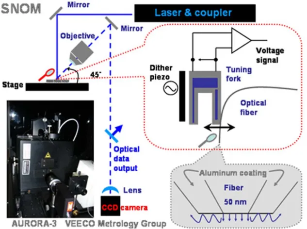
Instrument picture of the NSOM (Aurora-3), schematic of the light paths, tuning fork mechanism and the AFM tip are shown in Fig. 2.6 [8]. The Excitation laser source in an NSOM system is led into an optical fiber. The end of the fiber sharpened to a diameter of ~ 50 nm and coated with aluminum (approximately 100 nm thick) as a tip. A scanning probe microscope (SPM) equipped in an NSOM is comprised of a sensing probe (for scanning across the sample surface), piezoelectric ceramics (for positioning the sample), an electronics control unit and a computer (for controlling the scan parameters and generating images). A SPM has provided the technology needed to maintain the tip-sample spacing (typically less than 10 nm) while a tip scanning over a sample. Two modes (with different relative positions of photo detectors), transmission mode and reflection mode are available for different sample types in the SPM. Photo detectors are placed behind the sample (or beside the tip) for transmission mode (or for reflection mode) to collect light emitted from the sample. In the experiment illustrated in chapter 5, we use the reflection mode. A sensor
(with very high spatial resolution, and can sense height changes ~ 0.1 Ao ) is another important component in the SPM. There are two imaging modes (defined by the types of the sensor): Scanning Tunneling Microscopy (STM) and Atomic Force Microscopy (AFM) in the SPM. In our experiment (illustrated in chapter 5), the Aurora-3 operates in AFM non-contact mode and uses a tuning fork mechanism (a tuning fork mounted alongside the tip and made to oscillate at its resonance frequency) as a sensing probe. The AFM and NSOM images are simultaneously obtained. The excitation light is locally illuminated by a nano-aperture (~80 nm), the diameter of the fiber tip is about 250 nm, and the near-field signals were collected by an objective at the 45° normal to the sample surface.
Fig. 2.6 Instrument picture of the scan near field optical microscope (SNOM), schematic of
the light paths, tuning fork mechanism and the AFM tip (very close to the sample < 10 nm) are shown. The AFM image and the laser light reflection were obtained simultaneously. [8]
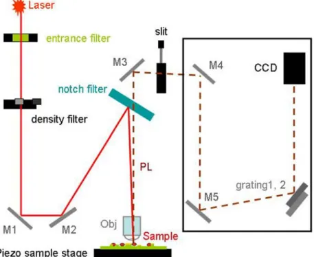
§ 2-4 Reflectance Spectrometer
Fig. 2.7 The schematic of optical system of the reflectance spectrometer [9]
The spectrometer (Model U-3010 [9]) is used for reflectance analysis of liquid, solid and gaseous samples in the ultraviolet-visible region (wavelength: 190 nm ~ 900 nm). Our relative experiments (Au coated SiNR array structures reflectance spectra) will be illustrated in chapter 5, 6 and 7. The optical system of the spectrometer is shown in Fig. 2.7 [9]. A light from the light source (the tungsten iodide (WI) lamp: in the visible region; the Deuterium (D2) lamp: in the ultraviolet region) is selected automatically by the light source switching mirror (optionally selectable in a range of 325 to 370 nm) according to the measurement wavelength. Then, the selected light passed a filter, reflected by a spherical mirror, passed an entrance slit, and let to the monochromator. The monochromator (with variable pitch stigmatic diffraction grating; the grating constant: 1/600 mm) is employing
unique stigmatic concave grating. After passed an exit slit, the monochromatic beam is branched into the reference beam and the sample beam (the reference beam and the sample beam are included in the sample compartment) by a group of sector mirrors (including two plane mirrors, two toroidal mirrors, and a rotating mirror). The beams which have passed through the sample compartment are let by two toroidal mirrors and two plane mirrors, and finally irradiated into the detector (the Photomultiplier tube (PMT)). The reflection value is obtained from the intensity value from the sample side/ the intensity value form the reference side.
Reference:
[1] HORIBA JOBIN YVON, HR800 User manual
[2] http://www.picoquant.com
[3] http://www.nanonics.co.il/index.php?page_id=149A
[4] Ash E.A. and Nicholls G. Nature 237, 510 (1972)
[5] http://en.wikipedia.org/wiki/Near-field_scanning_optical_microscope
[6] Lewis A., Isaacson M., Harootunian A., and Murray A. Ultramicroscopy 13, 227
(1984)
[7] Pohl D.W., Denk W., and Lanz M. Appl. Phys. Lett. 44, 651 (1984)
[8] AURORA-3 Instrument User Guide
[9] Instruction manual model U-2010/U-3010/U3310 spectrometer (maintenance manual),
Chapter 3 The Finite Element Method
The finite element method (FEM) [1-2] is commonly used for solving the partial differential equations over complicated domains and thus is a good choice for a wide class of problems. By breaking up the computational domain into elements (usually elements with simple shapes expressed by basic functions) and solving the unknown function within, one can approximately solve the partial differential equations over domains even with complicated geometries. For two-dimensional (2D) problems, the triangles or quadrilaterals elements are typically chosen. Segmenting the computational domain into small elements is called meshing. The meshing size should be tinny enough to ensure that the field interior to the meshing element can be approximated with sufficient exactness.
By the FEM, the approximations of the partial differential equations expressed by the expansions of unknown coefficients combined with the boundary conditions of each element lead to a matrix system of the form:
[ ]
A{ } { }
x = b , (3.1) where the matrix[ ]
A is square of size N×N, very sparse due to the continues properties on each joint (joint of two neighboring segments), and{ }
b is a column matrix determined on the basis of the boundary conditions or the forced excitation (current source, incident field, etc.) [2]. After Eq. (3.1) constructed, its solution proceeds easily with the application of an iterative or direct solver.Based on the electromagnetic theory, 2D FEM simulations are suitable for carrying out the near-field optical properties, especially the field distribution of the array structures. The localized surface plasmon (LSP) resonance modes relative topics in our research were investigated by this method (illustrated in chapter 4, 5, 6 and 7). We used the scattered harmonic propagation model provided by FEMLAB (www.femlab.de). The model solves
the electromagnetic fields based on Maxwell’s equations. For the example of TM incident mode, the z component of scattered field Escat in 2D (x-y) surface can be solved by:
z iz i z r i z r scat z r scat z r J i E k E E k E 2 0 0 2 0 ) 1 ( ) 1 ( ε ωμ μ ε μ ∇ − =−∇⋅ ∇ − + ⋅ ∇ . (3.2)
Where ε is the relative permittivity, r μ is the relative permeability, r ω is the angular frequency, μ0 is the permeability in vacuum, is the wave number in vacuum. is the z component of the incident electric field generated by . Where is the electric current source (or can be assumed as the excitation source).
0 k i z E iz J zˆ zˆJiz
To describe the FEM, the FEM will be illustrated by an one-dimensional (1D) example [2] in the following. The Sturm-Liouville problem which can be used to describe the potential or the electric field between the parallel plates will be used as the example to describe the method. The Sturm-Liouville equation is described as
a x x x f x U x q dx x dU x p dx d + = < < ⎟ ⎠ ⎞ ⎜ ⎝ ⎛ − ( ) ( ) ( ) ( ) ( ),0 . (3.3) Where is an unknown function (can be the potential or the electric field between the parallel plates), and are known functions. In order to solve the Sturm-Liouville problem by the FEM, we illustrate a weighted residual method for the approximation in every segment of the interested 1D line (x). Inside every segment (labeled as segment “m”), the following condition must be satisfied.
) (x U ) (x p q(x) 0 ) ( ) ( :
∫
= m W Domain m x R x dx W , (3.4) ) ( ) ( ) ( ) ( ) ( ) ( q xU x f x dx x dU x p dx d x R ⎟+ − ⎠ ⎞ ⎜ ⎝ ⎛ − = , (3.5)Where Wm(x) is the weighting function which must be chosen under the restriction of
[
]
<∞ ⎪⎭ ⎪ ⎬ ⎫ ⎪⎩ ⎪ ⎨ ⎧ ⎥⎦ ⎤ ⎢⎣ ⎡ +∫
W x dx dx d x W a x m m 0 2 2 ( ) ) ( (3.6)to prevent from the numerical errors (due to the divergence). is the residual function original from Eq. (3.3).
) (x
R
Substitute Eq. (3.5) into (3.4), and use the technique of integration by part, the weak form equation in the region 0 ~ xa is obtained:
0 ) ( ) ( ) ( ) ( ) ( ) ( ) ( ) ( 0 0 ⎥⎦ = ⎤ ⎢⎣ ⎡ − ⎥⎦ ⎤ ⎢⎣ ⎡ + −
∫
a a x m x m m m dx dU x W x p dx x f x W x U x W x q dx dU dx dW x p . (3.7) Let ) ( ) ( 1 2 1 x N U x U e i N e i e i e∑∑
= = = , (3.8) where ⎪⎩ ⎪ ⎨ ⎧ < < − − = ⎪⎩ ⎪ ⎨ ⎧ < < − − = . , 0 , ) ( ; , 0 , ) ( 1 2 1 2 1 2 2 1 1 2 2 1 otherwise x x x x x x x x N otherwise x x x x x x x x N e e e e e e e e e e e e (3.9)And then, substitute Eq. (3.9) into Eq. (3.8), one obtains
∑
= ⎥⎦ ⎤ ⎢ ⎣ ⎡ − − + − − = Ne e e e e e e e e e x x x x U x x x x U x U 1 2 1 1 2 1 2 2 1 ) ( (3.10) In Eqs. (3.8)-( 3.10), the superscript “e” is for the eth element, and the lower index “i” (1 or 2) are the two end points of a segment. For example, and are the two unknowns of the eth segment. The figure for explaining the eth segment and the linear shape functions is shown in Fig. 3.1.e
U1 U e
2
Finally, let Wm = N j, the following equation can be obtained:
[ ]{ }
e + i ij U A endpoint{ }
e i a b x = 0 (3.11) where dx x N x N x q dx x dN dx x dN x p A e e x x e j e i e j e i e ij∫
⎥ ⎥ ⎦ ⎤ ⎢ ⎢ ⎣ ⎡ + = 2 1 ) ( ) ( ) ( ) ( ) ( ) ( ,[ ]
, and. Every can be solved by Eq. (3.11).
⎥
⎦
⎤
⎢
⎣
⎡
=
ee e e ijA
A
A
A
A
22 21 2 12 11 dx x f x N b xee x e i e i ( ) ( ) 2 1∫
= e i UFig. 3.1 Illustration of the eth segment and the linear shape functions. [2]
If there are N elements of an interested line segment, there are N-1 nodes in between. If each element contains two unknowns ( and ), N elements will produce 2N unknowns. And between the neighboring two elements, the joint node must satisfy the continuous boundary condition. Since there are N-1 nodes inside the segment, number of unknowns is reduced to N+1. Reducing number of unknowns is an advantage of the FEM.
e
U1 U e
2
For 2D FEM, by the similar concept, one can start from the general form of the wave equation:
![Fig. 2.3 Jobin Yvon LabRam HR800, side view II [1]](https://thumb-ap.123doks.com/thumbv2/9libinfo/8629640.192259/37.892.186.731.107.502/fig-jobin-yvon-labram-hr-side-view-ii.webp)
![Fig. 2.4 The schematic diagram of fluorescence images and the lifetime measurement system [2]](https://thumb-ap.123doks.com/thumbv2/9libinfo/8629640.192259/39.892.154.765.141.488/fig-schematic-diagram-fluorescence-images-lifetime-measurement.webp)
![Fig. 2.7 The schematic of optical system of the reflectance spectrometer [9]](https://thumb-ap.123doks.com/thumbv2/9libinfo/8629640.192259/42.892.173.747.190.676/fig-schematic-optical-reflectance-spectrometer.webp)
![Fig. 3.1 Illustration of the eth segment and the linear shape functions. [2]](https://thumb-ap.123doks.com/thumbv2/9libinfo/8629640.192259/47.892.162.764.150.685/fig-illustration-eth-segment-linear-shape-functions.webp)
![Fig. 3.2 The computation domain and node coordinates for the eth triangle. [2]](https://thumb-ap.123doks.com/thumbv2/9libinfo/8629640.192259/49.892.131.785.177.998/fig-computation-domain-node-coordinates-eth-triangle.webp)
