Short-Duration Rapid-Thermal-Annealing Processing of
Tantalum Oxide Thin Films
Santhiagu Ezhilvalavan and Tseung-Yuen Tseng
* Department of Electronics Engineering and Institute of Electronics, National Chiao Tung University, Hsinchu-300, Taiwan, Republic of China The effect of the rapid thermal annealing (RTA) processingtime on the electrical properties of reactively sputtered tan-talum oxide (Ta2O5) films that was deposited onto Pt/SiO2/
n-Si substrates, which resulted in the formation of a metal–
insulator–metal (MIM) planar capacitor structure, was studied. The Ta2O5MIM capacitors were subjected to dif-ferent RTA processing times (30 s to 30 min) at tempera-tures in the range of 600°–800°C in an ambient oxygen-gas atmosphere. A very-short-duration RTA process at a tem-perature of 800°C in oxygen gas for 30 s crystallized the films, decreased the leakage current density (to 10−10A/cm2 at a stress field of 100 kV/cm), increased the dielectric con-stant (to 52), and resulted in the most-reliable time-dependent dielectric-breakdown characteristics. The de-crease in leakage current density was attributed to the reduction of oxygen vacancies and the suppression of sili-con diffusion from the SiO2/n-Si substrate into the Ta2O5 grain and the grain boundary, because of the shorter-duration annealing. Increasing the annealing time to >30 s increased the leakage current density. The annealing dura-tion of the RTA process was more crucial in regard to obtaining optimum dielectric properties and low leakage current densities. Time-dependent dielectric-breakdown characteristics indicated that Ta2O5 MIM film capacitors that were subjected to an RTA process at a temperature of 800°C for 30 s in oxygen gas can survive a stress field of 1.5 MV/cm for 10 years. The electrical and dielectric measure-ments in the MIM configuration showed that Ta2O5 is a good dielectric material and is suitable for use in future dynamic random-access memories.
I. Introduction
T
ANTALUM OXIDE (Ta2O5) films have been demonstrated to be highly promising storage dielectrics in the next genera-tion of dynamic random-access memories (DRAMs), because of their high dielectric constant and relatively good leakage current density.1–3Thermal treatments in various ambient en-vironments have been performed after Ta2O5film deposition, to reduce the leakage current and improve the quality of the film; these treatments include dry oxygen gas,4–6dry O3,7 UV-O2,8UV-O3,8,9UV-O3(UV-O2),8N2O plasma,10and oxygen-gas plasma.11 During thermal treatment in the oxygen-containing ambient environment, oxygen diffuses into the Ta2O5films, which leads to a decrease in the number of oxygen vacancies and a reduction of the number of weak spots in the Ta2O5 films.12 When Ta2O5 film is deposited onto silicon,
which forms a metal-oxide-semiconductor (MOS) capacitor structure, and is subjected to various post-deposition anneal-ings, the process results in the formation of an interfacial silica (SiO2) layer that has a low dielectric constant.13This event is one of the most serious problems for the application of Ta2O5 films to DRAM capacitors.
Rapid thermal annealing (RTA) is often used in the process-ing of semiconductor devices to minimize undesired diffusion and interfacial reactions.14,15Although there are some reports available in the literature about the RTA processing of Ta2O5 films, most of the research has been for Ta2O5films that have a MOS capacitor structure and the duration of the RTA treat-ment was maintained atⱖ60 s.16–22Also in the earlier reports, the importance of the RTA processing time on the leakage current density of Ta2O5 films was not studied in detail. Sun and Chen16,17demonstrated that Ta
2O5 films that have been treated via RTA in N2O are much less leaky than those that have been treated via conventional furnace annealing in oxygen gas. However, those researchers could only speculate about the reasons behind the improvement due to RTA treatment in N2O. Lau et al.18reported that RTA treatment in N
2O is more effi-cient than RTA treatment in oxygen gas, in regard to providing free oxygen atoms. However, those researchers could not dis-tinguish whether the decrease in silicon contamination or the decrease in oxygen vacancies was the principal factor that led to a lower leakage current. Pignolet et al.19observed a dielec-tric constant of 45 and leakage current density of 10−8A/cm2 for the RTA-processed reactively sputtered Ta2O5films. How-ever, those researchers did not study the effect of the RTA time duration on the leakage-current properties of Ta2O5 films. Ta2O5storage capacitor films on rugged polysilicon that had been treated via RTA treatment in oxygen gas were reported by Kamiyama et al.20and Lo et al.21 Their results showed that RTA treatment in oxygen gas reduces the density of the oxygen vacancies.
Very-short-duration (for ∼30 s) RTA processing of Ta2O5 films in an ambient oxygen-gas atmosphere, having a MIM planar capacitor structure, are not reported in the literature. Decreasing the processing time will restrict the diffusion of silicon atoms, and using the MIM structure permits the elimi-nation of the possible formation of the interfacial SiO2layer. In this investigation, we report the importance of the very-short-duration (30 s) RTA processing of Ta2O5film that is formed on a platinum-coated SiO2/n-Si substrate that has a MIM capacitor structure. Detailed investigation on the electrical and dielectric properties shows the high reliability and quality of the Ta2O5 film for possible incorporation into ultralarge-scale integration (ULSI) applications.
II. Experimental Procedure
The deposition of Ta2O5 thin films in this study was per-formed on Pt/SiO2/n-Si substrates, which forms a MIM planar capacitor structure via dc magnetron sputtering from a high-purity tantalum-metal target (diameter of 2.5 in.). More details on the deposition technique may be found in our earlier work.23 The sputtering gas was a mixture of 80% argon and 20% oxy-W. A. Schulze—contributing editor
Manuscript No. 190446. Received January 5, 1998; approved June 12, 1998. Supported by the National Science Council of ROC under Project No. NSC 86-2221-E-009-045.
*Member, American Ceramic Society.
Journal
gen, with a total pressure of 10 mtorr (∼1.33 Pa). The purity of the gas was ascertained by using the same procedure as that reported by Oehrlein et al.24During deposition, the chamber was first filled with argon gas and then was used to presputter the target clean for at least 5 min. Then, the argon/oxygen gases were introduced into the chamber to attain a total pressure of 100 mtorr (∼13.3 Pa). The substrates were not intentionally heated. The film thickness was estimated to be 100 nm by using both ellipsometry, with 632.8 nm wavelength He-Ne laser light source (Rudoph Research, Flanders, NJ), and an␣ stepper (Model 200, Tencor, USA); the thickness measurement was further verified by examining the cross section of the film via scanning electron microscopy (SEM). The platinum top electrode, with a thickness of 50 nm and a diameter of 350m, was patterned by using a shadow-mask process. The Ta2O5 capacitors were electrically characterized via computer control (Model HP4145B, Hewlett–Packard, Tokyo, Japan) for cur-rent–voltage (I–V) measurements. The dc leakage currents were evaluated using a step-voltage technique, and the mea-surement was performed with sufficient charging time to attain the steady-state dc leakage regime. The step-voltage technique, with a sufficiently long charging time, is generally accepted as revealing the most-accurate data.25
The capacitance–voltage (C–V ) characteristics and the di-electric loss tangent were measured at a frequency of 100 kHz with a sweeping signal of 0.5 V (ac), using an impedance–gain phase analyzer (Model HP4194A, Hewlett–Packard). RTA was performed in an RTA furnace (Model HPC 700, Ulvac Sinku-Rico, Tokyo, Japan) at temperatures in the range of 500°– 800°C for 30 s to 30 min in an ambient oxygen-gas atmo-sphere. The maximum heating rate (∼100°C/s) was used. The structure and impurities that were distributed in the Ta2O5 films were analyzed by using X-ray diffractometry (XRD) (Model D5000, Siemens, Munich, FRG), SEM (Model S250 microscope, Hitachi, Tokyo, Japan, fitted for energy-disper-sive X-ray analysis (EDX)), and secondary-ion mass spectrom-etry (SIMS) (Model IMS-4f, CAMECA, Courbevoie Cedex, France).
III. Results and Discussion
(1) Microstructural Features
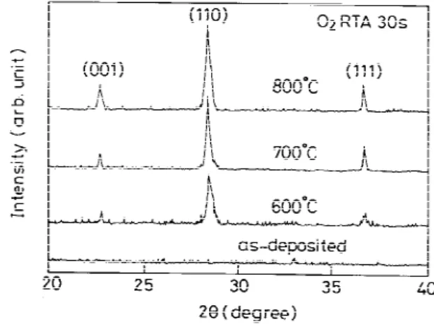
Figure 1 shows the XRD patterns of as-deposited Ta2O5 films that have been subjected to RTA at different temperatures (600°–800°C) for 30 s in an ambient oxygen-gas atmosphere. The as-deposited films were amorphous, and the films were crystalline when subjected to RTA treatment at temperatures ⱖ600°C for 30 s. The crystallinity increased as the annealing temperature increased, in terms of an increase in the intensity of the diffracted peaks, whereas the thickness of the film was
maintained at a constant value. The XRD spectra of the films in Fig. 1 correspond either to-Ta2O5(the orthorhombic crys-tal structure) or␣-Ta2O5(a high-temperature form of Ta2O5).26 This uncertainty occurs because the spectra of the two phases are too similar to allow distinction between them on the basis of XRD alone.26,27In the RTA processing of amorphous films, during crystallization, the excess free energy of the amorphous state, relative to the crystalline phase, is released instanta-neously, which results in explosive crystallization. Such a pro-cess often produces much-higher temperatures than the set val-ues instantaneously in a localized area and provides a probable opportunity for the Ta2O5to transform to the ␣-phase.14,15,19 Because our RTA processing time is very short and also be-cause the cooling and heating rates are very high (100°C/s, almost equivalent to normal quenching methods), we believe that there is a possibility of␣-phase formation; this phase can appear as a minor phase and may be distributed in the grain boundaries. Such two-phase structures have been mentioned in research by Pignolet et al.19on RTA-processed Ta
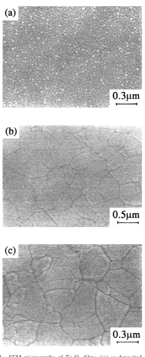
2O5films. SEM analysis readily shows that the as-deposited Ta2O5film is amorphous, whereas the annealed Ta2O5films are polycrys-talline. Figure 2 shows SEM micrographs of the amorphous Ta2O5thin film (Fig. 2(a)) and crystalline Ta2O5thin films that have been annealed at a temperature of 800°C for 30 s and 30 min (Figs. 2(b) and (c), respectively). The average grain size was estimated to be 0.3–1m. The grains for the film that was subjected to RTA processing for 30 s are angular and have thin grain boundaries, whereas the films that were annealed for a longer duration (∼30 min) exhibit larger grain-size distribu-tions. These results demonstrate that RTA that is conducted for a longer duration leads to sufficient grain growth; in contrast, RTA treatment for 30 s causes restricted grain growth and grain-boundary formation. This result is obvious because an RTA processing time of 30 s is very short and is too rapid for possible nucleation and growth kinetics to occur.
(2) Electrical Characteristics
Figure 3 shows the I–V characteristics of Ta2O5 thin-film MIM capacitors that have been subjected to RTA processing for 30 min in an ambient oxygen-gas atmosphere at tempera-tures of 600°, 700°, and 800°C. The leakage current of amor-phous Ta2O5is lower than that of polycrystalline Ta2O5films that have been annealed at higher temperatures for a long time (30 min). The as-deposited amorphous Ta2O5films show good electrical properties, in terms of leakage current density (10−10 A/cm2at a stress field of 100 kV/cm) and dielectric constant (31). The leakage current that flows through the Ta2O5 film increases from 10−10A/cm2 to 10−7 A/cm2following the an-nealing. Detailed analysis of the leakage-current mechanisms of amorphous and polycrystalline Ta2O5films at different elec-tric-field regimes were reported in our recent paper.23The in-crease in the leakage current density in the crystallized film is attributed to silicon that has penetrated into the Ta2O5grain and the grain boundary from the underlying SiO2/n-Si substrate material.
Figure 4 shows the variation in the leakage current density with the applied electric field for the Ta2O5 films that have been subjected to RTA processing at different temperatures for 30 s in an ambient oxygen-gas atmosphere. The I–V curve shifts to a higher leakage current density as the annealing tem-perature increases, up to 700°C. Furthermore, increasing the annealing temperature to 800°C results in I–V characteristics with a very low leakage current. This phenomenon can be related to the degree of crystallization, because the as-deposited amorphous films begin to crystallize at temperatures ⱖ600°C and they undergo complete crystallization at a tem-perature of 800°C. This observation is supported by the XRD results, which indicate complete crystallization of the films that have been annealed at a temperature of 800°C (by way of a higher intensity of the diffracted peaks), in comparison to the films that have been annealed at temperatures of 600° or 700°C. In addition, RTA that is performed at higher
tempera-Fig. 1. XRD spectra of Ta2O5films as-deposited and processed via
RTA in oxygen gas at different temperatures for 30 s.
ture in an ambient oxygen-gas atmosphere provides greater grain growth and also corresponds to greater diffusion rates and greater amounts of oxidation, thereby decreasing the oxygen vacancies and, hence, reducing the leakage current density.
The effect of the RTA processing time duration—i.e., the holding time of the films at higher annealing temperature— on the leakage current property of Ta2O5films was also stud-ied. Figure 5 shows the leakage current density as a function of the RTA processing time of Ta2O5 films that have been pro-cessed at a temperature of 800°C in an ambient oxygen-gas atmosphere for 30–120 s. A shorter processing time (∼30 s) clearly leads to better electrical characteristics, by way of re-ducing the leakage current density from 10−7 A/cm2to 10−10 A/cm2at a stress field of 100 kV/cm. The present results dem-onstrate that a much-shorter duration of RTA processing (∼30 s) is sufficient for complete crystallization of the films and also for reducing the oxygen vacancies; the shorter RTA processing duration also minimizes the interface reactions through the grain boundaries.
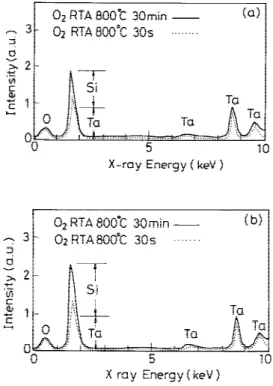
A large number of grain interiors and grain boundaries were scanned via EDX for possible differential distributions of sili-con between these regions (Fig. 6). The solid line in Fig. 6 represents the film that was subjected to RTA treatment at a temperature of 800°C in oxygen gas for 30 min, and the dotted line denotes the film that was subjected to RTA treatment for 30 s at a temperature of 800°C in oxygen gas. Typical EDX tracings indicate that silicon was detected both in the grain boundary and in the grain interior; the silicon distribution at the grain boundary was larger than that within the grain. The EDX distribution profile also shows that the silicon concentration in the Ta2O5films that were subjected to RTA processing for 30 s is very low, in comparison to that of films that were subjected to RTA processing for 30 min.
Fig. 2. SEM micrographs of Ta2O5 films ((a) as-deposited
amor-phous film, (b) film after RTA treatment for 30 s at 800°C in oxygen gas, and (c) film after RTA treatment for 30 min at 800°C in oxygen gas).
Fig. 3. Leakage current density versus applied electric field for amorphous and polycrystalline Ta2O5films processed via RTA for 30
min in an ambient oxygen-gas atmosphere at different temperatures.
Fig. 4. Leakage current density versus applied electric field for Ta2O5films subjected to RTA processing at different temperatures for
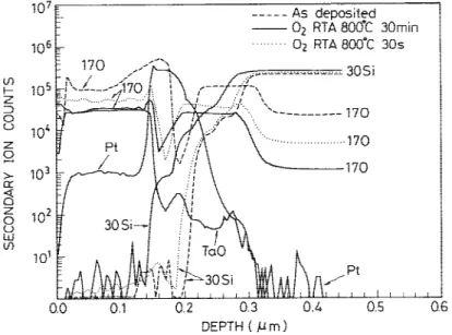
SIMS was performed on a set of Ta2O5/Pt/SiO2/n-Si samples to confirm the presence of silicon contamination in the Ta2O5 films that were subjected to RTA processing at high tempera-tures. Figure 7 shows the SIMS depth profile of the Ta2O5film on a Pt/SiO2/n-Si substrate. The dashed curve in the figure represents as-deposited Ta2O5film, the solid curve represents the Ta2O5film that was annealed at a temperature of 800°C for 30 min in oxygen gas, and the dotted curve represents the film that was subjected to RTA processing at a temperature of 800°C for 30 s in oxygen gas. A trace amount of silicon was
detected in the RTA-processed film. The film that was pro-cessed via RTA for 30 min in oxygen gas shows a higher silicon concentration and a lower oxygen concentration. Also, the silicon concentration at the interface is increased after an-nealing and it further extends into the Ta2O5film. In contrast, the film that was subjected to RTA processing for 30 s shows a lower concentration of silicon at the interface and in the film, in comparison to the Ta2O5film that was processed via RTA for 30 min. The reason for this difference is the underlying SiO2/n-Si substrate, from which silicon probably diffuses into the Ta2O5film through the very thin layer of platinum (1500 Å (150 nm)) during the high-temperature annealing. This result suggests that Ta2O5 crystallizes rapidly and silicon diffuses along the grain boundary and further penetrates into the grain. This result also suggests that the diffusion process of silicon is dependent on the temperature and the time duration of RTA processing. The details of the oxidation of these diffusing sili-con atoms—which results in an increased sili-concentration of oxy-gen vacancies, thereby increasing the leakage current of the polycrystalline Ta2O5 films—were reported in our earlier pa-per.23Because the presence of silicon is the only definite dif-ference between the amorphous and polycrystalline Ta2O5 films, we have given more attention to silicon, to clarify the leakage current that flows in polycrystalline Ta2O5films.
Impurity constituents that have limited solubility (e.g., sili-con) help to form coherent grain-boundary layers and will help to increase the density of trapping states, which influences the field dependence of the potential barrier very strongly at high electric fields and results in increased current density. This mechanism is very similar to that which occurs at the grain boundaries in classical varistor materials.28The Si4+anion that substitutes into the Ta5+site prefers a four-coordinated tetra-hedral site and is expected to form an acceptor state. Lau et
al.29reported the possible, energetically most-shallow defect state (0.3 eV) in Ta2O5on silicon capacitors, where its density increases as the post-deposition annealing temperature in-creases. This defect state is related to the silicon contamination from the silicon substrate. This observation is consistent with the present results, because our SIMS and EDX results clearly indicate the presence of silicon, both in the grain interior and in the grain-boundary regions. The significance of the present observation is as follows. The silicon concentration is in-creased by the RTA processing of the sputtered films in oxygen gas for long durations (ⱖ30 min). The diffused silicon atoms are then oxidized by the oxygen that is contained in Ta2O5 itself and is also supplied from the gas phase, which results in Ta2O5films with an increased concentration of oxygen vacan-cies, as shown in the following defect equation:
2SiO2共s兲→ Ta2O5
2Si⬘Ta+VO䡠 䡠 +4OO (1) Therefore, the presence of silicon is partially charge compen-sated by the oxygen vacancies, whereas the remaining oxygen vacancies continue to participate in enhancing the leakage cur-rent of the films that were annealed for long durations. In the case of very-short-duration (30 s) RTA processing of Ta2O5 films in oxygen gas, the amount of silicon diffusion is re-stricted to a smaller level and annealing in oxygen gas de-creases the number of oxygen vacancies, thereby reducing the leakage current density.
(3) Dielectric Constant
The dielectric constants of the Ta2O5films were calculated from the accumulation capacitance at a frequency of 100 kHz, the known area of the platinum electrodes of the MIM capaci-tor, and the ellipsometrically determined oxide thickness. Fig-ure 8 shows the dielectric constants and dielectric loss of Ta2O5 films as a function of RTA temperature for a duration of 30 s in an ambient oxygen-gas atmosphere. The effective dielectric constant of Ta2O5film that has been annealed at a temperature of 800°C is larger than that of films that have been annealed at temperatures of 600° or 700°C. Similarly, the loss factor shows
Fig. 6. EDX spectra for a Ta2O5thin film subjected to RTA
pro-cessing at 800°C for 30 s ((a) grain interior and (b) grain-boundary region).
Fig. 5. Leakage current density versus applied electric field for Ta2O5film after RTA processing at 800°C in oxygen gas for different
time durations.
an increase, from 0.01 to 0.017. This observation suggests that the fully crystalline film has a larger dielectric constant than the partially crystallized film. Furthermore, increasing the RTA processing time for a given RTA temperature results in an increase of the dielectric constant and the dielectric loss factor (from 0.012 to 0.035), as shown in Fig. 9. However, increasing the RTA processing time to >30 s increases the leakage current density (see Figs. 5 and 7). Hence, the best RTA processing time,∼30 s, was optimum for MIM Ta2O5 capacitor films to obtain a higher dielectric constant (52), yet preserving a rela-tively low leakage current density of 10−10A/cm2 at a stress field of 100 kV/cm.
Quite frequently, the dielectric constant that is reported for Ta2O5 film is ∼25–35. However, dielectric constants of >35 have also been reported in the literature.30,31For example, Wu
et al.30reported that their Ta
2O5films had a dielectric constant in the range of 20–45. Pignolet et al.19reported that a sample that was subjected to RTA processing in oxygen gas exhibited a dielectric constant of 45, and Lau et al.18observed that films
that were subjected to RTA processing in oxygen gas exhibited a dielectric constant of 40. Treichel et al.31reported that the dielectric constant is a function of the film thickness and the annealing parameters; they also reported that, for relatively thick Ta2O5films (>60 nm), a dielectric constant as high as 40 was possible.31 It should be noted that the Ta
2O5 films that have been used for the present study have a thickness of∼100 nm. Therefore, it may be realized that the dielectric constant of 52 that has been obtained for the present Ta2O5films is higher than that which is conventionally observed.
(4) Time-Dependent Dielectric Breakdown
Time-dependent dielectric breakdown (TDDB) is also called resistance degradation of dielectrics; this process shows a slow increase of leakage current under a dc field stress. TDDB is a characteristic of the intrinsic materials, the procedures, and the quality of the processing and electrode materials.32,33Lifetime extrapolation, by using constant voltage-stress time-dependent dielectric-breakdown studies, predicts a lifetime of 10 years at
Fig. 8. Plot of effective dielectric constant of Ta2O5film versus RTA temperature. Fig. 7. SIMS depth profiles of an amorphous Ta2O5thin film and polycrystalline Ta2O5thin films.
an operating voltage of 1.5 V. This result indicates that very-short-duration (30 s) RTA-processed film has a longer lifetime than that of film that has been annealed for a long duration (30 min). Figure 10 shows the lifetime extrapolation from the de-pendence of cumulative failure on TDDB stress time for Ta2O5 films that have been subjected to RTA processing for 30 min in oxygen gas. The plotted points follow straight lines, and ran-dom failure modes are not observed, which indicates that the sputtered MIM Ta2O5capacitors are of high quality and good uniformity. Repeated measurements for more films demon-strate that the films that were annealed for a long time (30 min) at a temperature of 800°C have the shortest breakdown time. Also, the breakdown time for amorphous or partially crystal-lized films (such as that which was subjected to RTA process-ing at a temperature of 600°C for 30 min in an oxygen gas) is
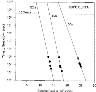
longer than that of films that were subjected to RTA processing for 30 min in oxygen gas for temperatures of 700° or 800°C. Higher temperature and longer RTA processing times lead to more grain growth (Fig. 2) and higher silicon diffusion into the grain and the grain-boundary region (Fig. 3), which results in increased leakage current density; these factors are considered to be responsible for the shorter TDDB lifetimes. TDDB life-time characteristics for the Ta2O5films that were subjected to RTA processing for a very short time (30–120 s) in oxygen gas are shown in Fig. 11. The Ta2O5film capacitor that was sub-jected to RTA processing for 30 s in oxygen gas seems to have a longer lifetime than films that were subjected to RTA pro-cessing for 30 min in oxygen gas. The extrapolated long-term lifetime indicates that Ta2O5MIM capacitors that are subjected to RTA processing for 30 s at a temperature of 800°C in oxy-gen gas can survive 10 years at a stress field of 1.5 MV/cm.
Fig. 9. Plot of effective dielectric constant of Ta2O5film versus RTA processing time.
Fig. 10. TDDB lifetime, as a function of electric field, for Ta2O5
films processed via RTA in oxygen gas for 30 min at different temperatures.
Fig. 11. TDDB lifetime, as a function of electric field, for Ta2O5
films processed via RTA in oxygen gas at 800°C for 30–120 s.
IV. Conclusions
We have investigated the electrical characteristics of tanta-lum oxide (Ta2O5) thin films that have been deposited on Pt/ SiO2/n-Si substrates (forming a metal–insulator–metal (MIM) planar capacitor structure) and their improvement via very-short-duration high-temperature rapid thermal annealing (RTA) processing, from the standpoint of application to ultra-large-scale integrated (ULSI) circuits. Present results demon-strate that a longer processing time (∼30 min) results in in-creased leakage current density, whereas a shorter processing time (30 s) leads to lower leakage characteristics. Very-short-duration RTA processing is sufficient for the complete crys-tallization of the films; yet, it minimizes the interface reactions through the grain boundaries. The decrease in leakage current density is attributed to the reduction of oxygen vacancies and the suppression of silicon diffusion from the SiO2/n-Si sub-strate into the Ta2O5grain and the grain boundary, because of the shorter annealing time. Time-dependent dielectric break-down characteristics indicate that Ta2O5MIM film capacitors that are subjected to RTA processing for 30 s in oxygen gas can survive 10 years at a stress field of 1.5 MV/cm. It can be concluded in the present experiment that RTA processing at a temperature of 800°C for 30 s in an ambient oxygen-gas at-mosphere is the most effective method for simultaneously maintaining a large dielectric constant and a lower leakage current density.
References
1M. Saitoh, T. Mori, and H. Tamura, “Electrical Properties of Thin Ta
2O5
Films Grown by Chemical Vapor Deposition,” Tech. Dig.—Int. Electron De-vices Mater., 680–83 (1996).
2W. R. Hitchens, W. C. Krusell, and D. B. Dobkin, “Tantalum Oxide Thin
Films for Dielectric Applications by Low Pressure Chemical Vapor Deposi-tion,” J. Electrochem. Soc., 140 [9] 2615–21 (1993).
3Y. Numasawa, S. Kamiyama, M. Zenke, and M. Sakamoto, “Ta
2O5Plasma
CVD Technology for DRAM Stacked Capacitors,” Tech. Dig.—Int. Electron Devices Mater., 43–48 (1989).
4S. Zaima, T.. Furuta, Y. Yasuda, and M. Iida, “Preparation and Properties of
Ta2O5Films by LPCVD for ULSI Application,” J. Electrochem. Soc., 137 [4]
1297–300 (1990).
5E. Kaplan, M. Balog, and D. Frohman-Bentchkowsky, “CVD of Ta
2O5
Films for Monolithic Capacitor Applications,” J. Electrochem. Soc., 123 [10] 1570–73 (1976).
6M. Matsui, S. Oka, K. Yamagishi, K. Kuroiwa, and Y. Tarui, “Photo-process
of Tantalum Oxide Films and Their Characteristics,” Jpn. J. Appl. Phys., 27 [4] 506–11 (1988).
7C. Isobe and M. Saitoh, “Effect of Ozone Annealing on the Dielectric
Properties of Tantalum Oxide Thin Films Grown by Chemical Vapor Deposi-tion,” Appl. Phys. Lett., 56 [10] 907–909 (1990).
8S. Tanimoto, M. Matsui, K. Kamisako, K. Kuroiwa, and Y. Tarui,
“Inves-tigation of Leakage Current Reduction of Photo-CVD Tantalum Oxide Films Accomplished by Active Oxygen Annealing,” J. Electrochem. Soc., 139 [1] 320–28 (1992).
9H. Shinriki, M. Nakata, Y. Nishioka, and K. Mukai, “Two Step Annealing
Technique for Leakage Current Reduction in Chemical Vapor Deposited Ta2O5
Films,” IEEE Electron Device Lett., 10, 514–16 (1989).
10H. S. Park, Y. K. Baek, J. C. Kim, S. H. Choi, and K. H. Oh, “Effect of Post
Deposition Annealing and Electrode Materials on the Characteristics of Tanta-lum Oxide Films Deposited by Plasma Enhanced Chemical Vapor Deposition”; pp. 524–29 in Extended Abstracts of the International Conference on Solid State Devices and Materials. Semiconductor Research and Development Laboratory, Hyundai Electronics, Ichon-ku, Kyoungki-Do, South Korea, 1992.
11S. Kamiyama, H. Suzuki, H. Watanabe, A. Sakai, M. Oshida, T. Tatsumi,
T. Tanigawa, N. Kasai, and A. Ishitani, “Ultra-thin TiN/Ta2O5/W Capacitor
Technology for 1 Gbit DRAM,” Tech. Dig.—Int. Electron Devices Mater., 49–54 (1993).
12H. Shinriki and M. Nakata, “UV-O
3and Dry O2: Two Step Annealed
Chemical Vapor Deposited Ta2O5Films for Storage Dielectrics of 64-Mb
DRAMs,” IEEE Trans. Electron Devices, 38 [3] 455–62 (1991).
13S. Shinriki, Y. Nishioka, Y. Ohji, and K. Mukai, “Oxidized Ta
2O5/Si3N4
Dielectric Films on Poly-crystalline Si for DRAMs,” IEEE Trans. Electron Devices, 36 [2] 328–32 (1989).
14R. Singh, “Rapid Isothermal Processing,” J. Appl. Phys., 63 [8] R59–R114
(1988).
15H. Hu, C. J. Peng, and S. B. Krupanidhi, “Effect of Heating Rate on the
Crystallization Behaviour of Amorphous PZT Thin Films,” Thin Solid Films,
223, 327–33 (1993).
16S. C. Sun and T. F. Chen, “Leakage Current Reduction in Chemical Vapor
Deposited Ta2O5Films by Rapid Thermal Annealing in H2O,” IEEE Electron.
Devices, 17 [7] 355–57 (1996).
17S. C. Sun and T. F. Chen, “A Novel Approach for Leakage Current
Re-duction of LPCVD Ta2O5and TiO2Films by Rapid Thermal N2O Annealing,”
Tech. Dig.—Int. Electron Devices Mater., 333–36 (1994).
18W. S. Lau, P. W. Qian, N. P. Sandler, K. A. Makinley, and P. K. Chu,
“Evidence that N2O is a Stronger Oxidizing Agent than O2for the Post
Depo-sition Annealing of Ta2O5on Si Capacitors,” Jpn. J. Appl. Phys., 36 [2] 661–66
(1997).
19A. Pignolet, G. Mohan Rao, and S. B. Krupanidhi, “Rapid Thermal
Pro-cessed Thin Films of Reactively Sputtered Ta2O5,” Thin Solid Films, 258,
230–35 (1995).
20S. Kamiyama, T. Saeki, H. Mori, and Y. Numasawa, “Highly Reliable
Technology for 256 Mbit DRAMs,” Tech. Dig.—Int. Electron Devices Mater., 827–30 (1991).
21G. Lo, D. L. Kwong, P. C. Fazan, V. K. Mathews, and N. P. Sandler,
“Highly Reliable, High-C DRAM Storage Capacitors with CVD Ta2O5Films
on Rugged Polysilicon,” IEEE Electron Devices Lett., 14 [5] 216–18 (1993).
22F. C. Chiu, J. J. Wang, J. Y. Lee, and S. C. Wu, “Leakage Currents in
Amorphous Ta2O5Thin Films,” J. Appl. Phys., 81 [10] 6911–15 (1997).
23S. Ezhilvalavan and T. Y. Tseng, “Conduction Mechanisms in Amorphous
and Crystalline Ta2O5Thin Films,” J. Appl. Phys., 83 [9] 4797–801 (1998).
24G. Oehrlein, F. d’Heurle, and A. Reisman, “Some Properties of Crystallized
Tantalum Pentoxide Films on Silicon,” J. Appl. Phys., 55 [10] 3715–25 (1984).
25G. W. Dietz, M. Schumacher, R. Waser, S. K. Streiffer, C. Basceri, and
A. I. Kingon, “Leakage Currents in Ba0.7Sr0.3TiO3Thin Films for Ultra
High-Density Dynamic Random Access Memories,” J. Appl. Phys., 82 [5] 2359–64 (1997).
26A. S. Pavlovic, “Some Dielectric Properties of Tantalum Pentoxide,” J.
Chem. Phys., 40 [4] 951–56 (1964).
27A. Reisman, F. Holtzburg, M. Berkenblit, and M. Berry, “Reactions of the
Group VB Pentoxides with Alkali Oxides and Carbonates. III, Thermal and X-ray Phase Diagrams of the System K2O or K2CO3with Ta2O5,” J. Am. Chem.
Soc., 78, 4514–20 (1956).
28S. Ezhilvalavan and T. R. N. Kutty, “High-Frequency Capacitance
Reso-nance of ZnO-based Varistor Ceramics,” Appl. Phys. Lett., 69 [23] 3540–43 (1996).
29W. S. Lau, K. K. Khaw, P. W. Qian, N. P. Sandler, and K. P. Chu, “Defect
States Responsible for Leakage Current in Ta2O5Films on Si due to Si
Con-tamination from the Substrate,” J. Appl. Phys., 79 [11] 8841–43 (1996).
30X. M. Wu, S. R. Soss, E. J. Rymaszewski, and T. M. Lu, “Dielectric
Con-stant Dependence of Poole–Frenkel Potential in Tantalum Oxide Thin Films,” Mater. Chem. Phys., 38 [3] 297–300 (1994).
31H. Treichel, A. Mitwalsky, N. P. Sandler, D. Tribula, W. Kern, and A. P.
Lane, “Low Pressure Chemical Vapor Deposition of Tantalum Pentoxide Films for ULSI Devices Using Tantalum Pentaethoxide as Precursor,” Adv. Mater. Opt. Electron., 1 [6] 299–308 (1992).
32M. S. Tsai and T.-Y. Tseng, “Effect of Oxygen to Argon Ratio on the
Properties of (Ba,Sr)TiO3Thin Films Prepared by rf Magnetron Sputtering,” J.
Appl. Phys., 82 [7] 3482–87 (1997).
33R. Waser, T. Baiatu, and K.-H. Ha¨rdtl, “dc Electrical Degradation of
Perovskite-Type Titanates: I, Ceramics,” J. Am. Ceram. Soc., 73 [6] 1645–53