0-7803-8436-9/04/$20.00 ©2004 IEEE 51 9th Int’l Symposium on Advanced Packaging Materials
Packaging of Cu/Low-k IC Devices: a Novel
Surface Passivation and Direct Fine-Pitched Gold
Wirebond Ball Interconnects Analysis
Surasit Chungpaiboonpatana
1,2, Frank G. Shi
1, G. P. Li
11The Henry Samueli School of Engineering, University of California, Irvine, CA 92697 2Mindspeed (Conexant) Inc., 4300 MacArthur Blvd., Newport Beach, CA 92660
Abstract—The trend towards finer pitch and higher
performance devices has driven the semiconductor industry to incorporate copper and low-k dielectric materials. Compared to the commonly used aluminum metallization scheme on the traditional silicon dioxide and/or silicon nitride passivation, a Cu/low-k combination offers higher on-chip communication speed and a lower overall device cost. But the process of packaging Cu/low-k devices has been proven to be difficult, relying either on additional lithography and deposition steps or on costly new process tools. Thus, this work presents a novel methodology to bond fine pitch Au wire directly onto the Cu/low-k pad structure using the industry standard tool set. A Cu/k test vehicle is designed with the required slotted low-k fillings for dual damascene CMP process need. In addition, a thin organic passivation film is developed for coating the exposed Cu/low-k pad temporarily from copper oxidation and to provide a wirebondable surface to form the proper interconnects. A design of experiment is performed to optimize wirebonding parameters (power, time, and USG bleed), along with key physical contributors from wafer sawing and die attaching steps that impact the interconnect shear strength and quality. In addition, electrical and optical characterization and surface failure analysis are performed to confirm the feasibility of the technology. Finally, reliability results of the pad structure design and recommendations for further process optimization are presented.
I. INTRODUCTION
Copper has better electrical conductivities (resistivity of 1.7µΩ-cm) and electromigration resistance (107 A/cm2 electromigration limit) than aluminum (resistivity of 3.0µΩ-cm and 106 A/cm2 electromigration limit). In fact, in the latest generation of aluminum interconnects copper is the prevalent doping and implantation material applied to improve electromigration properties to the overall interconnect scheme [1]. However, the challenge to integrate copper lies in its inability to form interconnects in a normal wirebond operating condition since it is readily oxidized [2]. Though typically having a lower heat of formation than most materials used in semiconductor manufacturing, copper thermodynamically forms superlattice structure with gold material. Under the liquidus temperature range, Cu-Au readily forms ordered-disordered solid solution and relatively few metastable intermetallic phases. The reasons are that both Cu and Au are face cubic centered (FCC) and have similar lattice size, valence, and electronegativity, as opposed to the Au-Al system where
many complex intermetallic phases are formed [3]. The equilibrium phases for typical wirebonding condition are noted as either AuCu or Au3Cu type, and both phases imposed reliability concerns because of their ductile and brittle nature to Au wire material [4].
This study introduces a novel method to wirebond the most widely accepted gold ball bond interconnects directly onto the Cu/low-k terminal pad. Both the copper and the low-k structure utilized here are derived from the standard fabrication schemes offered by leading foundries and IDMs (Integrated Device Manufacturer). Contributing factors and parameters adjustments to the front- and the back-end processes post CMP (Chemical Mechanical Polishing) passivation and fine pitch wirebonding processes are described and experimented. Furthermore, formed interconnects are analyzed by shear testing, pad cratering identification, detailed surface analysis, and electrical and thermo-mechanical study. As a reference, industry JEDEC requirements for ball bond strength and package level reliability are used. Lastly, experimental findings are discussed and improved process implementations are recommended.
II. PROCESS SET UPS AND EXPERIMENTS A. Cu/Low-k Test Vehicle’s Structure and Critical Surface Preparations
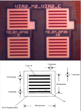
A daisy chained test vehicle is designed using the 0.15um Cu technology node as the standard fabrication process. Specifically, the 1.5mm x 0.5mm test die has been gang arrayed with two signal copper layers connected through interlayer tungsten vias. In addition, the test wafer is backgrinded to the standard 14mils thickness so that the test die can be configured into the encapsulated 5x5mm 24 leads PQFP ceramic package. Fig. 1 shows the pad layout structure in the test die that incorporates both copper metallization and low-k material. Each pad layout is fabricated in a combed pattern filled with the Applied Material’s Black Diamond low-k material. The pad opening from silicon oxy-nitride passivation is 90um x 90um and each slotted low-k material is 5um wide with the edge-to-edge distance of 10um. A thin film of Ti/TiN/Al deposited between each low-k structure and the copper metallization serves as an adhesion and diffusion layer. As specified by the industry’s recommended dual damascene design rules,
52 9th Int’l Symposium on Advanced Packaging Materials this slotted pattern helps minimize the recession and dishing
effects during the CMP step [5]. However, this required low-k CMP pattern reduces the metallization and interdiffusion area for wirebonding. Typically, a bonded interconnect requires a fully metallized surface for adhesion and intermetallic formation. Thus, this reduced Cu surface demands wirebond tool adjustment and surface optimization for reliable bonds to form. These two approaches are discussed more in the next section.
Fig. 1. Cu/low-k bonding pad pattern and its corresponding features’ dimensions.
Prior to sawing and wirebonding, the wafer is processed by the Synergy post-CMP cleaning tool to remove copper’s native oxides. Next, an organic preservative material is added to the cleaning chemistry to form an inherent thin-film structure on the exposed copper pad. This protective coating uses Benzotriazole (BTA) preservatives and is deposited through employing parameters adjustment on the solution pH, the cleaning concentration, and the scrub type [6]. Based on many studies about BTA organic coating as a corrosion inhibitor, its self-limiting reaction in thin film thickness, and the capability of the post CMP tool to uniformly coat the full 8-inch wafer surface within three sigma control, a 100 Angstrom coating is applied. This experiment serves to confirm if such thickness can helps reduce exposed Cu metal oxidation so that wirebonding is feasible. Specifically, the thin organic film needs to have the capability to withstand sawing, cleaning, and curing processes temporarily and maintain a surface condition for bond parameters to be applicable during the subsequent wirebond step. In addition, after wirebonding, residual films should not be present as a new interface between the die and the encapsulated mold compound due to potential reliability concerns. This is noted in BTA’s vaporization
temperature at around 204°C. A detailed analysis of the surface analysis and the direct wirebonding reliability using this pad passivation approach is reviewed in the discussion section.
B. Die Attach Curing and Wirebonding Design of Experiment
Though the copper surface is coated with a thin film passivation layer, curing temperature and duration still need to be minimized to lower the oxidation growth rate beneath the coating [7]. Both conventional (135 minutes at 155ºC) and snap cure (15 minutes at 175ºC) conductive materials are compared in the die attach process. These die attach materials are chosen for their flexibility and compatibility to the wirebonding experiment needs. In addition, they are capable to withstand high temperature processes with very low moisture absorption
The snap cure material (Ablebond 2300) is selected to die attach the Cu/low-k test vehicle due to its relatively much shorter thermal exposure time. Apparent from the diagram, this material application results in less oxidation growth on the thin-film passivated area even at a higher curing temperature. Moreover, Ablebond 2300 material possesses other favorable properties for this experiment such as high temperature tolerance (up to 260ºC), low stress, and ultra-low moisture absorption (0.22%) post cured [8]. Furthermore, published studies indicate that there is an initial incubation period where oxidation on copper is purely the brittle Cu2O. This starting stage is reaction-controlled and dependent on time, thermal activation energy, and environment of the exposure. As the heating time extends, the mass-controlled process begins with Cu2O growth which gradually self-limits its thickness pending the Cu deposition processes. However, it further oxidizes into a darkened CuO type with a maximum thickness depending on the diffusion condition and the surface properties [9]. Since the thermal activation energy of the 155 versus 175ºC is relatively similar, the difference of 120 minutes between the two die attach materials is the key to promote oxidation growth of the matured CuO type. The experiment on the die attach materials helps confirm these findings and is thus used as the basis for the snap cure material choice.
After the die attach process, the configured test vehicle is submitted to the Kulicke and Soffa’s (K&S) 8000 series wirebond tool. This wirebonder is chosen for its long wire (7.6 mm), fine pitch (45um), flexible loop height (up to 100 um), and tight bond placement (+/- 3.5 um) capabilities. Although this tool is well-calibrated to bond down to 45 um fine pitch, the standard 1.0 mil AW-99 wire on the 60 um bond pad pitch parameters operating at 150ºC/100KHz is used here to mimic the current industry’s high volume production experience. Ultra fine pitch wirebond applications and study will be introduced in the near future. Moreover, AW-99 wire (i.e., 99.99% pure Au wire in the 4N modulus category) is appropriate for high strength fine pitch wirebonding purposes. It has very high ductility and minimal hardening properties suitable for thinner and
53 9th Int’l Symposium on Advanced Packaging Materials mechanical-damage prone pad structure. Furthermore, K&S
8000 series wirebonder is optimized for the AW-99 wire type utilization [10]. To perform wirebonding, key parameters obtained from publicized experiments with bond formation potential (e.g., USG bleed, bond power, and bond time) are used to fine-tune welding parameters. Furthermore, ranges for each parameter are based on pre-experimental findings and tool suppliers’ recommendations. In addition, these settings are initially selected from production experience to minimize pad or the silicon structure damage underneath.
III. RESULTS AND DISCUSSION A. Surface Passivation Analysis
Thermo-desorption gas chromatography mass spectrometer (TD-GCMS) and sequential electrochemical reduction analysis (SERA) tools are utilized to examine the passivated Cu/low-k pad surface and its oxidation formation during the key assembly process. TD-GCMS characterization method helps detect BTA organic species using relative mass calculation while SERA tool detects accurate Cu oxide types and their corresponding thicknesses through the electrochemical reduction method [11].
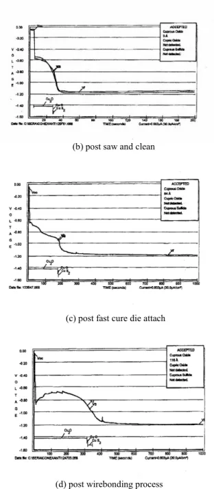
The four SERA results of a passivated Cu/low-k pad in Fig. 2 vary in copper oxide types and thicknesses after the passivation, the saw cleaning, the fast cure die attaching, and the wirebonding steps. Categorically, the pad surface has only 4 Angstroms of pre-matured cuprous oxide (Cu2O) after passivation. Then, the cuprous oxide thickens slightly to 9 Angstroms after the sawing and cleaning steps. It appears that copper oxidation under the thin-film of BTA is not significantly affected by either humidity or mechanical processes here. Yet, the cuprous oxide grows exponentially to 64 Angstroms following the first thermal exposure in the fast curing die attach step. This confirms that temperature does impact copper oxide growth even with organic preservative present. With many models attempting to simulate copper oxide growth on bare metallized surface, this study is the first to witness this fundamental phenomena with low-k dielectric present under organic passivation. Lastly, after wirebonding step, the cuprous oxide grows further to 116 Angstroms.
(a) post passivation
(b) post saw and clean
(c) post fast cure die attach
(d) post wirebonding process
Fig. 2. SERA results of passivated Cu/low-k after each key assembly step. In clock-wise direction, results are after passivation process in Figure 2(a), after saw cleaning in 2(b), post fast cure die attaching in 2(c), and after wirebonding step in 2(d).
BTA film presence after wirebonding is a concern to the overall reliability performance since it is an additional interface between the die and the mold encapsulant compounds. Its adhesion properties during stress testing in the reliability chambers and at the customer board level surface mount are still unknown. Therefore, it is necessary not to introduce this new interface during the evaluation stage. To confirm this, the unbonded pads of post wirebonding test vehicle are subjected to the thermal desorption GC-MS tool to detect if thin BTA film still present. This study uses the tool’s common profile library
54 9th Int’l Symposium on Advanced Packaging Materials for BTA organic compound comparison and detection. The
total ion and the extracted ion chromatographs from the pad surfaces are plotted and compared with the mass spectrums from the reference. From the library profile, BTA peaks at 20:26 minutes and mass (m/z) at 119. The chromatograph result indicates no BTA trace found after wirebonding. This implies that the assembly processes and thermal exposures until the wirebonding step have the pad surfaces protected from mature cupric oxide formation.
However, without BTA’s presence after wirebond step, the copper surface is then exposed fully to the environment leading to drastic copper oxide growth that eventually will interact to the mold compound post encapsulation. Thus, a fundamental understanding of bare copper oxide growth rate and types is then applicable here. The impact of the oxidation level without inhibitor film on long term package reliability is tested in the following section.
B. Reliability and Failure Mode Analysis
Both electrical and thermo-mechanical reliability tests in this study help evaluate the quality of the bonding to the passivated Cu/low-k pad structure. Preliminary electrical testing delineates the device level EM characterization procedures and specifications. Ten devices are subjected to the interconnect EM testing of 40mA for 200 hours at 125°C device operating environment. All ten vehicles do not exhibit any package level openings, shorts, or leakages. However, failure occurs when there are open vias at the die interconnect level confirmed using cross-sectional analysis. Though this initial test result shows migration-resisting bonds being formed, it does not truly represent the bonding interface EM characteristic. Accordingly, a future study is in plan to incorporate higher driving current and operating temperature to simulate welded interfacial conditions.
The thermo-mechanical testing involves reliability stressing a set of test vehicles that have gone through the experimental process and set-up. Essentially, the preconditioning, high temperature storage (HTS), thermal cycling (TC), and unbiased highly accelerated stress testing (HAST) are performed. The results of the electromigration and thermo-mechanical reliability stressing listed in Table I are intended to uncover the weakest link in this technology implementation.
Table I
Electromigration and Reliability Stressing Results of Direct Cu/low-k Wirebond Vehicles
Test Descriptions Conditions Failing Units Preconditioning Level 3 (30ºC/60%RH
192 hours)
0/66 Electromigration 40mA at 125ºC for 200
hours 0/10
High Temperature
Storage 150ºC for 1000 hours 0/22 Thermal Cycling -55 to 125ºC at 1000
cycles 0/22
Unbiased HAST 85ºC/85% at 136 hours 0/22
The test vehicles pass both the device level EM test and the thermo-mechanical stress tests imposed by the TC, HTS, and unbiased HAST. The initial concern of the exposed copper pad surface interacting with the mold encapsulant compound seems to be reduce by the high temperature selected, the minimum stress/warpage, and the very low moisture absorption material utilized. In addition, since copper metallization has been used for many decades in the assembly package area (e.g., extensive interaction with OSP, soldermasks, and other organic-based compounds), several baseline material properties have been developed to accommodate the copper material.
The interconnect is analyzed further by subjecting the sampling units from each reliability testing to decapping (with sulfuric/nitric acid) and ball shearing. Though significant reduction in shear values resulted, all parts sheared with greater than 15g minimum baseline force. Noted that these bonds are sampled sheared prior to stressing with a range of 25-28gf. The analysis note that many of the welded bonds show ‘skid’ and ‘squash’ phenomena even with shear strength in the 16-18gf range post stressings. This is attributed to the exposed low-K surface. In addition, although the BTA is confirmed by GC-MS that no principle composition remained, minor constitutes from decomposed BTA material post wirebonding step may present an inherent low-K or Cu surface interaction that causes difficult bond welding. Further analysis of this phenomenon and wirebond fine-tuning are required to develop this process technology for a robust manufacturing environment.
The EDX surface analysis reveals a widespread presence of Au-Cu superlattice on the bonded pad area and no IM or metallic phase formation in the low-k slotted area. This indicates that the bond formed over the low-k surface is not of chemical bonding, but a physical wire adhering to the pad. As a result, the shear mode mechanism is different from the typically formed Al-Au alloy phase IM structures. Additionally, traces of Ti and Al in the deposited Cu/low-k adhesion and diffusion barrier layer can be seen in low-k area EDX shots. This is visible in the EDX analysis since the shear mechanism is likely to cause anti-CMP dishing low-k structure and the thin film barrier layer to residual on other pad areas. This study can further extend to evaluate different shear settings (height, speed, and tip type) of Dage tool and their differences in the Au-Cu shear value.
The prevalent material detected in the low-k area is silicon. This is the backbone structure of Black Diamond low-k material. It is also interesting that TC and HTS stressed bonds tend to shear through the Au-Cu solid solution and/or the superlattice to Au wire interface region more than the EM or the unbiased HAST tested parts do. The latter is sheared prevalently more toward the Au wire and the Cu/low-k pad interface since the relatively higher and longer thermal exposure time in the TC and the HTS reliability tests will induce more superlattice formation. Evidently, studies have shown that longer aging and thermal
55 9th Int’l Symposium on Advanced Packaging Materials exposure time tends to increase the IM/superlattice phase
thickness. Also, interconnect’s brittleness is often the result of this newly formed interface to Au wire despite being a superlattice solid solution [2,4,12,13].
Another contributing factor may be that the amount of humidity exposure during the unbiased HAST stressing does not affect significantly with the material set and the final bond reliability. Therefore, using a high temperature tolerant and very low moisture absorption material set can make parts resistant to moisture-induced stress and/or delamination even with the exposed Cu/low-k pad. Furthermore, with the copper’s tensile strength higher than that of Au and the minimum IM/superlattice formation, the bond shear failure mode for EM and unbiased HAST tests tends to occur more on the weaker interface, namely the Au wire and Cu/low-k pad interface. Future extension of this study is to analyze the IM/superlattice growth mechanism and various phase transformations with incremental thermal exposure time on the exposed Cu/low-k pad structure.
Since the surface area that generally allows the IM/superlattice structure formation is reduced by the slotted low-k material, alternate options to increase the contact surface area and still maintain the CMP dishing/recession requirements are being investigated. As indicated in both pad structure designs in Fig. 3, the bonding pad area is dedicated with pure copper metallization. The slotted low-k structure also has gone through extensive simulation to limit it from the bonding area yet maintain its CMP process manufacturability. This investigation intends to help further improve this novel process technology implementation.
Fig. 3. Potential improved Cu/low-k pad structure designs
undergoing investigation. The partial slotted and combed areas are low-k material embedded in the Cu pad. Top figure displays part of the pad structure with slotted low-k on the side, and bottom figure shows adifferent combed low-k structure allocated on all pad sides
V. CONCLUSION AND RECOMMENDATION This study presents a novel methodology to wirebond Au wire directly onto the exposed Cu/low-k pad. The method calls for industry standard wafer and assembly tool set utilization to ensure the manufacturability of the process. In addition, a thin organic passivation coating is developed to help reduce the exposed Cu/low-k pad oxidation level so that the matured black CuO formation is limited until the wirebonding step is completed. Next, test vehicle is designed, fabricated, and assembled using industry-selected material set that accommodate high temperature and low moisture/warpage requirements. Then, these test vehicles are subjected to the JEDEC level of reliability and electromigration tests. Through this study, appropriate CUSH saw blade, extra cleaning cycles, fast/snap cure die attach, and relatively higher wirebond parameter settings are recommended to achieve proper strength and reliable interconnects. Results on the viable process implementation of this technology in a production mode are revealed in the surface and failure analysis. They indicate that the Au-Cu superlattice formation is related directly to the available surface area of the exposed metallization, operating environment, and the length of thermal exposure time. In particular, the extended temperature exposure time significantly impacts the IM/superlattice growth and eventually the shear failure mode mechanism. There are several directions this study can be extended further. Specifically, future analyses of passivation properties on extended Cu/low-k thermal exposure, detail DOE and shear optimization through response model regression analysis, and the IM/superlattice phase transformation along with its impact on the overall reliability of interconnect can be researched. These studies can help improve this technology’s manufacturability further and enhance the
56 9th Int’l Symposium on Advanced Packaging Materials understandings of the fundamental mechanism inherent in
this developed process.
ACKNOWLEDGMENTS
The authors would like to thank Carlos Macias of Conexant, Dr. Craig Davidson of Flextronics, Dr. Hugh Li and Dr. Diane Hymes of Lams Research, and Dr. Nikhil Murdeshwar of K&S for their contributions in the experiment and several technical discussions.
REFERENCES
[1] S. P. Murarka and S. W. Hymes, “Copper Metallization for ULSI and Beyond,” Critical Reviews in Solid and Material
Sciences, vol. 20, no. 2, pp. 87-95, 1995.
[2] G. Harman, Wirebonding in Microelectronics: Materials,
Processes, Reliability, and Yield, 2nd ed., NY: McGraw Hill, 1997.
[3] H. Okamoto and T. B. Massalski, Eds., Binary Alloy Phase
Diagrams. Metal Park, OH: ASM International, pp. 358-362,
1990.
[4] Lee, Tran, et. al. “Thermal Aging Study on Both Au-Cu and Al-Al Wire Bond Interfaces,” Proc. of 53rd Elec. Component
and Tech. Conf. (ECTC), New Orleans, LA, May 2003, pp.
1761-1766.
[5] B. Zhao and F.G. Shi, “Chemical Mechanical Polishing in IC Processes: New Fundamental Insights,” Proc. of 4th Int.
Chem. Mech. Planarization for ULSI Multi-Level Intercon. Conf. (CMP-MIC), Santa Clara, CA, pp. 13-22, 1999.
[6] Diane Hymes, Hugh Li, Eugene Zhao, and John De Larios, “The Challenges of the Copper CMP Clean,” Semiconductor
Inter., New York, pp. 117-122, 1998.
[7] V. Brusic, M. A. Frisch, B. N. Eldridge, F. P. Novak, F. B. Kaufman, B. M. Rush, and G. S. Frankel, “Copper Corrosion With and Without Inhibitors,” J. Electrochem. Soc., vol. (138), no. 8, pp. 2253-2259, August 1991.
[8] Ablebond 2300 is the trademarked product of Ablestik (National Starch & Chemical Company) Inc., http://www.ablestik.com, 2003.
[9] H. A. Miller, “Copper Oxide Films,” J. of American Chem.
Soc., vol. 56, pp. 2626-2629, 1937.
[10] K&S 8000 series, AW-99 wire, and CUSH saw blade are the trademarked products of Kulicke & Soffa Industries Inc., http://www.kns.com, 2003.
[11] P. Bratin, M. Pavlov, G. Chalyt, and R. Gluzman, “New Application of the SERA Method – Assessment of the Protective Effectiveness of Organic Solderability Preservatives,” Proc. of Technical Conf. on Surf. Finish. ’95, pp. 538-589, 1995.
[12] Richard Ulrich, Jay Im, Phil Garrou, and Dan Scheck, “Thermosonic Gold Wirebonding to Electroless-ly Metallized Copper Bondpads over Benzocyclobutene,” Proc.
Int. Conf. on High Density Packag. and MCMs, pp. 260-265,
1999.
[13] G. Harman, “Wirebonding to Multichip Modules and Other Soft Substrates,” Pro. Int. MCM Conf., Denver, pp. 292-298, 1995.