Catalytic Growth of Silicon Nanowires Assisted by Laser Ablation
Yi-Han Yang, Sheng-Jia Wu, Hui-Shan Chiu, Ping-I Lin, and Yit-Tsong Chen* Department of Chemistry, National Taiwan UniVersity, Taipei 106, Taiwan, ROC, and Institute of Atomic and Molecular Sciences, Academia Sinica, P.O. Box 23-166, Taipei 106, Taiwan, ROC ReceiVed: May 28, 2003; In Final Form: October 23, 2003
Silicon nanowires (SiNWs, diameter g 5 nm, and length ∼ µm) have been fabricated with metal- and SiO2-catalyses assisted by laser ablation. In the catalytic growth of single-crystalline SiNWs by pure metal catalysts
(Fe, Ru, and Pr), Si{111}is found to be the most stable plane and wire growth axis is along〈111〉. The
growth mechanism follows a vapor-liquid-solid process, and the synthesized SiNWs typically have metal-tips composed of metal and Si, such as FeSi2, RuSi3, and PrSi4, respectively. In sharp contrast, a crystalline
growth axis of〈111〉and a wire growth axis of〈112〉are the result in the SiNWs catalyzed by SiO2. Besides,
the SiO2-catalytic SiNWs generally have no tips at the wire ends. Distinctive growth mechanisms resulting
from metal- and SiO2-catalyses will be discussed. Pressure effect on the longitudinal and transverse growing
rates in the fabrication of SiNWs has been examined.
1. Introduction
The optical and electrical properties of semiconductor-based nanostructures have recently stimulated tremendous research interest. A distinctive feature for semiconductor-based nano-structures relative to bulky material is the well-known quantum confinement effect owing to the reduced size and/or
dimen-sionality.1-3Silicon (Si) is an important semiconductor material
with its contemporary microelectronic technology being one of the greatest successes for the past century. Nevertheless, there is still room for improvement in the applications of Si-based optoelectronic devices. For instance, Si is an indirect band-gap (∼1.1 eV) material with a small exciton binding energy (∼15 meV), and does not emit visible light. For this reason, a great deal of effort has been made lately to fabricate lower
dimen-sional nanostructures,4-6such as quantum wells, nanowires, and
quantum dots,2,3 in which the motion of charge carriers is
confined, causing an increase of the band gap7and/or a
trans-formation of the electronic band structure from an indirect band gap to a direct one.
The advance of nanotechnology has led to a way to fabricate semiconductor materials from micro- to nanometers in size. Among other developments, more and more syntheses for one-dimensional nanowires have been accomplished. For Si, in particular, intensive research of one-dimensional nanowires and their corresponding optical and electrical properties has been
done by several groups, such as Lee,8-20 Lieber,21-26 and
Yu.12,13,27-37In the research studies approached by these groups, the wirelike crystalline nanostructures of Si were often fabricated
via vapor-liquid-solid (VLS) growth,38,39in which a liquid
cluster of metal-catalyst provides energetically favored sites for the absorption/adsorption of gas-phase reactants. The sizes of the catalysts are considered to be responsible for diameters of the resultant silicon nanowires (SiNWs). Based on this cor-respondence, the application of laser ablation to vaporize a target sample of bulky Si, mixed with metal catalyst, and to form small
sizes of nanoclusters in the initial VLS process is a unique and quite powerful method in the fabrication of one-dimensional SiNWs.
Different from the SiNWs catalyzed by metal nanoclusters via the VLS mechanism, another process for the nucleation and growth of SiNWs, catalyzed by silicon dioxide (SiO2), has been
reported by Lee and co-workers in laser ablation8,12-16as well
as in thermal evaporation.9-10,17-20 In this work, we will
investigate the catalytic roles of different metal catalysts (Fe,
Ru, Pr, RuCl3, and Pr6O11) and SiO2in the syntheses of SiNWs
assisted by laser ablation. From these comparisons, we have tried to discern the growth mechanism via SiO2-catalysis from that via the VLS in traditional metal-catalytic processes. Differences in the crystalline and wire growth axes of SiNWs have been examined for the SiO2- and metal-catalytic SiNWs. 2. Experiment
The apparatus used in our catalytic-growth experiments assisted by laser ablation is depicted in Figure 1. An evacuated alumina tube, placed inside a furnace, contains a target sample of Si powder (Acros, 325 mesh, 99+%) and metal catalyst. We have used iron (Fe) powder (Prochem, 325 mesh, 99.9%), ruthenium (Ru) powder (Strem, 99.9%), praseodymium (Pr) powder (Strem, 40 mesh, 99.9% REO), ruthenium chloride (RuCl3) powder (Strem, anhydrous, 47.44% Ru), and praseody-mium oxide (Pr6O11) powder (Strem, 99.9% Pr), respectively,
as metal catalysts. Alternatively, SiO2 (Aldrich, 325 mesh,
99.6%) was regarded as another supplying source for Si, and had also been introduced in the target sample. Totally, we have carried out six experiments, including Si + Fe, Si + Ru, Si +
Pr, Si + SiO2+ Fe, Si + SiO2 + RuCl3, and Si + SiO2+
Pr6O11, respectively, as reacting ingredients. In the experiments
without SiO2in the target sample, Si powder and metal catalyst
(Fe, Pr, or Ru) were mixed with a weight ratio of 90:10%. When
SiO2 was used in the growth of SiNWs, the weight ratio of
Si/SiO2/metal compound (Fe, Pr6O11, or RuCl3) was typically 45:45:10%.
The sample mixture was pressed into a pellet, placed in a crucible/quartz holder, and located in the center of the alumina * Author to whom all correspondence should be addressed at Institute
of Atomic and Molecular Sciences, Academia Sinica, P.O. Box 23-166, Taipei 106, Taiwan. Fax: +886-2-2362-0200. E-mail: [email protected]. sinica.edu.tw.
10.1021/jp030663d CCC: $27.50 © 2004 American Chemical Society
Published on Web 12/19/2003
Downloaded by NATIONAL TAIWAN UNIV on September 3, 2009 | http://pubs.acs.org
tube across the heating furnace (Figure 1). At one end of the alumina tube, an S1-UV window was attached for the pass of the laser beam; at the other, a water-cooling copper-finger and a Si-substrate were prepared for the collection of synthesized SiNWs. Before elevating the temperature, the alumina tube was
evacuated, and then heated to 850°C for the tube-wall degassing
for 2 h. As such, impurities coated on the target sample can also be removed. After degassing, temperature was elevated gradually to reach a point depending on the catalyst used, e.g.,
a eutectic temperature of FeSi2at 1207°C if Fe was employed
as a catalyst, or 1212°C when Pr was used. Argon (Ar) as a
carrier gas with a typical total pressure of ∼500 Torr and a
flow rate of 50 sccm was maintained throughout the experiment. When the gas flow reaches steady, a pulsed Nd:YAG laser (Spectra Physics, GCR-190) with 1064 nm wavelength, 30 Hz
repetition rate, and∼70 mJ/pulse was ignited to ablate the target
sample. The laser beam passing through a lens of 100-cm focal length was confined into 1.5 mm in diameter on the target sample. A computer programmed alignment-control for the mirror-mount has been designed to guide the laser beam moving from one spot on the target sample to another during the ablation process. As such, the laser could ablate fresh sample-spots in the course of experiment. The reaction time ranges from a half to a few hours. Finally, a dark yellow-colored spongelike product was collected from the cold surface of the copper-finger, the Si-substrate, and the inside wall of the alumina tube as well. Morphologies of as-synthesized SiNWs have been taken from a scanning electron microscope (SEM) and a transmission electron microscope (TEM). The SEM morphologies of SiNWs were performed in (1) JEOL JSM-6300 SEM with Link EXL II EDX, (2) Hitachi S-800 Field Emission SEM, and (3) LEO l530 Field Emission Gun SEM, and Energy Dispersive Spec-trometer (FEG-SEM + EDS). The TEM images of SiNWs were carried out by JEOL JEM-1200EX II TEM at 80 kV and Hitachi H-7100 TEM at 75 kV. High-resolution transmission electron microscope (HRTEM) images of SiNWs were obtained by a Philips Tecnai F30 Field Emission Gun TEM (FEG-TEM) with an EDAX Energy Dispersive X-ray Spectrometer at 300 kV, JEOL 2010 Analytical TEM at 200 kV, and JEOL JEM-4000EX HRTEM at 400 kV.
3. Results and Discussion
3.1. Nanowire Synthesis. Catalyses by Fe and SiO2. In the fabrication of SiNWs using Fe as a catalyst, the target sample for laser ablation is composed of Si/Fe ) 90:10% (weight ratio).
Alternatively, SiO2was supposed to be another supplying source
for Si. We also used samples of Si/SiO2/Fe ) 45:45:10% as reactants. The morphological contrasts in SEM, TEM, and
HRTEM between the SiNWs synthesized by Si + SiO2+ Fe
and those by Si + Fe are shown, respectively, in the left and right sides of Figure 2.
Figure 2a shows the SEM image of SiNWs resulting from
the reaction of Si + SiO2 + Fe at 500 Torr of Ar carrier
pressure, where the diameters of SiNWs range from 50 to 300 nm and the lengths are expressed in micrometers. By
compari-son, Fe-catalytic SiNWs fabricated without SiO2in the target
sample are shown in Figure 2b. Without SiO2, the synthesized SiNWs possess a sharper distribution in wire-diameter. Metal-tips have also been found at the fabricated SiNWs, marked in part by arrows in Figure 2b, indicating a catalytic growth following the VLS mechanism.
TEM morphology in Figure 2c shows that the majority of
the SiNWs, fabricated from Si + SiO2 + Fe, contain
bead-(marked by arrows in Figure 2c) and wire-like nanostructures where the beadlike nanoparticles/nanoclusters are embedded in Figure 1. Apparatus for the catalytic-growth experiments of SiNWs
assisted by laser ablation.
Figure 2. (a) SEM morphology of the SiNWs fabricated from Si + SiO2+ Fe, where the diameters of SiNWs range from 50 to 300 nm and the lengths are micrometers. (b) SEM morphology of the SiNWs catalyzed by Fe only, where the SiNWs are quite uniform. Parts of metal-tips at the SiNWs are marked by arrows. (c) TEM image for the SiO2-catalytic SiNWs of∼25 nm diameter. The beadlike nanoparticles/ nanoclusters (marked by arrows) comprise Si, O, (molar ratio, Si/O ) 1:2), Cu (background of the Cu grid for TEM measurement), and a negligible amount of Fe as revealed by an EDS analysis (inset). (d) TEM image of an Fe-catalytic SiNW. The composition of the tip attached to the wire is FeSi2as determined by EDS (inset). (e) HRTEM image shows the (11h1) crystalline plane with d-spacing of 0.32 nm in a SiO2-catalytic SiNW. The [11h1] crystalline growth axis is perpen-dicular to the wire growth axis of [1h12]. The crystalline Si core and amorphous SiOxsheath are also visualized. (f) HRTEM morphology for Fe-catalytic SiNW. From the ED pattern (upper-left inset) recorded along the [110] zone axis, the wire grows along the [1h11h] direction and (1h11h) lattice planes are of 0.32-nm d-spacing (upper-right inset).
Downloaded by NATIONAL TAIWAN UNIV on September 3, 2009 | http://pubs.acs.org
the nanowires or bridging sequential wire-sections. To under-stand details about the growth mechanism, energy dispersive spectroscopy (EDS) was taken to analyze the chemical com-position of the fabricated SiNWs. The inset of Figure 2c shows an EDS for the beadlike nanoparticles/nanoclusters, which comprise Si, O, (molar ratio, Si/O ) 1:2), Cu (background of the Cu grid for TEM measurement), and a negligible amount of Fe. The absence of Fe in the beadlike nanoparticles/ nanoclusters indicates that the growing is unlike a general process complying with an ordinary VLS mechanism, where metal-catalyst is often found to appear at the tip, root, or middle of synthesized nanowires. In sharp contrast, SiNWs synthesized from Si + Fe have distinct Fe-head and Si-wire-body as shown in Figure 2d. An EDS analysis (inset of Figure 2d) reveals that the tip of the SiNW is mainly composed of FeSi2. This composition agrees very well with the phase diagram of Si-Fe binary elements under the present experimental condition. In addition to the distinctive structures resulting from the pres-ence/absence of SiO2, diverse morphologies such as belt-, whisker-, and fishbone-like nanostructures are also found in the Fe-catalytic SiNWs (not shown).
An HRTEM image gives the microstructures about the inner core and outer sheath of the SiNWs fabricated from Si + SiO2 + Fe (Figure 2e), which depicts an outer sheath of ∼9 nm
thickness and a crystalline core of∼8 nm diameter. From the
HRTEM image in Figure 2e, the crystalline growth axis of the
SiNWs is along the [11h1] direction with d-spacing of 0.32 nm.
The wire growth axis directs to [1h12], which is determined by
an electron diffraction (ED) measurement (not shown). The (11h1) crystalline planes of SiNWs are parallel to the [1h12] wire growth axis, as can be seen in Figure 2e and tabulated in Table 1. It is noted that the majority (92%) of the SiNWs fabricated
from Si + SiO2+ Fe (weight ratio ) 45:45:10%) contain wire
growth axis along [1h12] and the minority (8%) of them orient
at [11h1] (Table 1). On the other hand, wire growth axis of the
SiNWs fabricated from Si + Fe is all along [1h11h](Figure 2f),
indicating that the (1h11h) crystalline planes are perpendicular to
the wire growth axis.
The distinctive wire growth axes of [1h12] and [1h11h] in the
fabricated SiNWs (Figures 2e and 2f), respectively, from Si + SiO2+ Fe and Si + Fe, indicate that different mechanisms have
been followed with or without SiO2in the reactant ingredients.
In an earlier study by Lee and co-workers,8,9 SiO2 was put
forward as a catalyst, and the SiO2-containing reaction to fabricate SiNWs does not comply with an ordinary VLS
mechanism. While the catalytic role of SiO2will be discussed
later in section 3.2, competition between SiO2and Fe as catalysts
in the fabrication of SiNWs has been observed in the present
experiment. In the fabrication from Si + SiO2+ Fe, the yield
ratio of 92:8% (Table 1) for the SiNWs of〈112〉and〈111〉wire
growth axes resulting from the catalyses of SiO2 and Fe,
respectively, is out of proportion to the weight ratio of SiO2/Fe ) 45:10% in the initial target-sample. This abnormal product/ reactant ratio may suggest an easier reaction, either
thermody-namically or kinetically, for Si + SiO2than for Si + Fe in the
fabrications of SiNWs.
Despite the different wire growth axes, the SiNWs catalyzed
by pure Fe (Figure 2f) have the same Si-core and SiOx-sheath
nanostructure as those catalyzed by SiO2 (Figure 2e). The
oxygen could be due to the relatively low vacuum (∼1 mTorr)
in the reaction tube. The Fe-catalytic SiNW (Figure 2f) has a
crystalline Si core of∼36 nm in diameter and an amorphous
SiOxouter-layer of∼5 nm in thickness. The 0.32 nm crystalline
spacing observed in the inner core of Fe-catalytic SiNWs
(upper-right inset of Figure 2f) corresponds to the d-spacing of Si{111}
lattice planes. In the Fe-catalytic growth of SiNWs, the Si{111}
crystalline planes are reported to be most stable.27 The ED
pattern from the inner core of SiNW (upper-left inset of Figure
2f) indicates that the SiNW has a [1h11h] wire growth axis
perpendicular to the (1h11h) lattice planes (Table 1). The wire
extruding from the FeSi2-tip and growing along the 〈111〉
direction (Figures 2d and 2f) provides clear evidence for the VLS mechanism in the SiNW synthesis. This result is consistent
with previous studies by Wagner39and Lieber and co-workers21
that the crystalline growth axis of〈111〉is most favorable in
the metal-catalytic fabrication of SiNWs via VLS processes. The crystalline growth axis, wire growth axis, tip composition,
wire crystallization, Si core diameter, and SiOxsheath thickness
for the Fe- and SiO2-catalytic SiNWs are listed in Table 1 for comparison.
Catalyses by Ru and SiO2. We have also synthesized SiNWs
with samples of Si + SiO2+ RuCl3(45:45:10%) and Si + Ru
(90:10%), respectively, and conveyed the SEM, TEM, HRTEM, ED, and EDS of these fabricated SiNWs in the upper and lower parts of Figure 3. Like what we discussed earlier, when both
RuCl3 and SiO2 coexist as catalysts, SiO2 plays a dominant
catalytic role over RuCl3 that could partly result from its
prevailing abundance in the reacting sample. In general, the
SiNWs fabricated from the mixture of Si + SiO2+ RuCl3have
∼10-50 nm diameters, appreciable wire-length, and no apparent metal-tips were found to attach at the ends of SiNWs (Figure 3a). For detailed investigation, the TEM image of the SiO2-catalytic SiNWs shown in Figure 3b further demonstrates uniformity in the diameters (12-15 nm) of as-grown SiNWs. The SiO2-catalytic SiNWs, again, have core-sheath micro-structure, as can be seen in HRTEM morphology (Figure 3c),
TABLE 1: Growth Direction, Composition, Crystallization, and Dimension of Catalytically Synthesized SiNWs
reacting ingredients
Si + Fe Si + Ru Si + Pr S i+ SiO2+ Fea Si + SiO2+ RuCl3b Si+SiO2+ Pr6O11c
crystalline growth axis [1h11h] [11h1] [1h11h] [11h1] [11h1] [11h1]
wire growth axis [1h11h] [11h1] [1h11h] [1h12] [1h12] [1h12]
tip composition FeSi2 RuSi3 PrSi4 SiOx SiOx SiOx
wire crystallization single single single + poly single single single
Si core diameter ∼36 nm ∼5 nm ∼16 nm ∼8 nm ∼5 nm ∼15 nm
SiOxsheath thickness ∼5 nm ∼9 nm ∼3 nm ∼9 nm ∼10 nm ∼5 nm
aRatio of 92:8% is found for the fabricated SiNWs with [11h1] crystalline growth axis and [1h12] wire growth axis catalyzed by SiO
2to those with [1h11h] crystalline growth axis and [1h11h] wire growth axis catalyzed by Fe. This column represents the major product of SiO2-catalytic SiNWs. bRatio of 92.3:7.7% is found for the fabricated SiNWs with [11h1] crystalline growth axis and [1h12] wire growth axis catalyzed by SiO
2to those with [11h1] crystalline growth axis and [11h1] wire growth axis catalyzed by RuCl3. This column represents the major product of SiO2-catalytic SiNWs.cRatio of 95.5:4.5% is found for the fabricated SiNWs with [11h1] crystalline growth axis and [1h12] wire growth axis catalyzed by SiO
2 to those with [1h11h] crystalline growth axis and [1h11h] wire growth axis catalyzed by Pr6O11. This column represents the major product of SiO2 -catalytic SiNWs.
Downloaded by NATIONAL TAIWAN UNIV on September 3, 2009 | http://pubs.acs.org
where the Si core (∼5 nm in diameter) is distinctly smaller than
the outer amorphous SiOxsheath (∼10 nm). The small diameter
of the Si core is comparable to those SiNWs fabricated from
zeolite.20 From the HRTEM in Figure 3c, the (11h1) lattice
fringes with d-spacing of 0.32 nm is observed. The wire growth
axis, along the [1h12] direction, can be identified from the ED
pattern as depicted in the inset of Figure 3c. These SiNWs
catalyzed by SiO2 have almost no contamination from the
metallic catalyst according to EDS analysis (not shown); neither has any metallic tip been found in the wires. This outcome again
suggests that SiO2plays a dominant catalytic role in the growth
of SiNWs from Si + SiO2+ RuCl3similar to the previous case
of Si + SiO2+ Fe. The fabricated SiNWs also have〈112〉and
〈111〉 wire growth axes at a ratio of 92.3:7.7%, once more,
indicating the competition of catalytic roles between SiO2and
RuCl3in the reaction. It is noteworthy that RuCl3decomposes
into Ru and Cl2at high temperature,40and the reduced Ru, as
a catalyst subsequently, is responsible for the fabricated SiNWs
of〈111〉wire growth axis.
For Ru-catalytic SiNWs, the SEM morphology is quite similar to that of SiO2-catalytic SiNWs (Figure 3a). Figure 3e shows a typical HRTEM image for the wire-body of a Ru-catalytic SiNW
with a [11h1] wire growth axis perpendicular to the Si (11h1)
crystalline planes (d ) 0.32 nm). The SiNW contains a metal-tip as depicted in the upper-right inset of Figure 3e. The metal-tip is
composed of RuSi3revealed from an EDS measurement (Figure
3f). It is interesting to note that the Ru-catalytic SiNWs contain
a heavy amorphous SiOxouter-shell around the RuSi3-tip. The
SiNWs have a very thin crystalline Si core (only ∼5 nm in
diameter) and relatively thick amorphous outer-sheath (∼9 nm
in thickness) (Figure 3e and Table 1). The thick SiOxsheath is
owing to the higher oxidation potential for Ru than that for Si
(despite the quite easy oxidation ability for Si itself).41Moreover,
an ED pattern for the wire-tip recorded along the [110] zone axis (lower-left inset of Figure 3e) provides information about the tip-composition of Si and Ru. The growth direction, composition, crystallization, and dimension of Ru- and SiO2-catalytic SiNWs are also tabulated in Table 1.
In addition to the filamentary nanowires, some interesting coil-like structure is also present in the products fabricated from
Si + SiO2+ RuCl3(Figure 3d). The TEM image in Figure 3d
shows that the coiled SiNW is of∼30 helical pitches, ∼30 nm
wire-diameter, ∼32 nm pitch-length, and ∼50 nm
coil-diam-eter. From HRTEM (inset of Figure 3d), the coiled SiNW is revealed to be single crystalline with a growing axis normal
to the Si {111} lattice planes (0.32 nm d-spacing). The Si
bonding in the helical SiNWs is an interesting subject to be studied in future. Referring to the very recently discovered bent SidSidSi structure in trisilaallene containing a formally
sp-hybridized Si atom,42the structural characterization of Si atoms
in the presently observed helical SiNWs will be very intriguing to be unraveled.
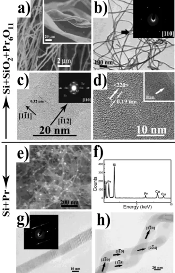
Catalyses by Pr and SiO2. Microscopic images, ED, and EDS
analyses for the SiNWs fabricated from Si + SiO2+ Pr6O11
and Si + Pr samples are shown in the upper and lower parts of Figure 4, respectively. Once more, the synthesized SiNWs from
Si + SiO2+ Pr6O11are catalyzed dominantly by SiO2(95.5%)
and lesser by Pr6O11(4.5%) (Table 1). In addition to the normal
SiNWs (SEM morphology in Figure 4a), helical belts (inset of
Figure 4a) have also been synthesized from Si + SiO2+ Pr6O11.
The dimensions for the helical belts are∼60 µm pitch-length,
∼40 µm belt-width, and ∼3 µm belt-thickness. TEM morphol-ogy of the SiO2-catalytic SiNWs (Figure 4b) shows a narrow
distribution of wire diameter at∼30 nm. The inset of Figure
4b gives a selected-area electron diffraction (SAED) pattern for the SiNW (marked by an arrow in Figure 4b) with the electron beam along the [110] zone axis. While the SAED in Figure 4b shows a single crystallite for the SiNW, plane defects could occasionally be observed in TEM images (not shown). The crystalline structure of SiNWs can further be visualized in the HRTEM image of Figure 4c.
From the HRTEM lattice image of SiO2-catalytic SiNWs
(Figure 4c), crystalline Si (11h1) planes are observed with
d-spacing of 0.32 nm, and wire growth axis orients to the [1h12] direction. Moreover, this SiNW has the crystalline-core and amorphous-sheath structure similar to those SiNWs catalyzed
by SiO2discussed earlier. Analysis for the SAED pattern (inset
of Figure 4c), taken from a spot in the wire-core, shows the
coexistence of the {111}, {220}, and {311} lattice plane
Figure 3. (a) SEM morphology of the SiNWs fabricated from Si + SiO2+ RuCl3, where the SiNWs have a sharp diameter distribution at ∼35 nm and tens of micrometers in length. (b) TEM morphology of SiO2-catalytic SiNWs with diameters at 12-15 nm. (c) HRTEM image of the SiO2-catalytic SiNW shows the crystalline Si core of∼5 nm diameter, [11h1] crystalline growth axis with d-spacing of 0.32 nm, and [1h12] wire growth axis. (d) TEM morphology depicts a coil-like SiNW of∼30 helical pitches, ∼30 nm wire-diameter, ∼32 nm pitch-length, and∼50 nm coil-diameter. The coiled SiNW is single crystalline with the growing axis normal to the Si {111} lattice planes (0.32 nm
d-spacing in the inset). (e) HRTEM image of a Ru-catalytic SiNW
with an ultrathin Si core of∼5 nm diameter and a very thick SiOx amorphous outer-shell (upper-right inset). Crystalline Si (11h1) planes with 0.32 nm d-spacing are perpendicular to the [11h1] wire growth axis. An ED pattern (lower-left inset), recorded along the [110] zone axis, reveals the crystalline structures of Si and Ru for the tip of the wire. (f) EDS spectrum for the tip of the Ru-catalytic SiNW shown in the upper-right inset of 3e. Except for the O and Cu signals belonging to the background, the composition of the wire-tip is RuSi3.
Downloaded by NATIONAL TAIWAN UNIV on September 3, 2009 | http://pubs.acs.org
families. This observation was further confirmed by an XRD
measurement (not shown). The [11h1] crystalline growth axis is
perpendicular to the [1h12] wire growth axis as indicated by
HRTEM and the ED pattern along the [110] zone axis (Figure 4c).
In addition to the Si{111}crystalline planes,{220}planes
have also been constructed in SiNWs with d-spacing of 0.19
nm (Figure 4d). Such {220} planes, however, appear only
occasionally in the crystalline Si cores. Taking a closer look at the magnified HRTEM image (inset of Figure 4d), defects due to micro-twins exist. The micro-twins often locate at the turning section when the growth of SiNW changes direction, consistent with a previous report that micro-twins occur usually in the kinks
of SiNWs.30
By comparison, the Pr-catalytic SiNWs, as depicted in Figure 4e, are very different in morphology from those catalyzed by SiO2. The Pr-catalytic SiNWs have quite uniform diameters of ∼30 nm, and contain metal-tips (white spots in Figure 4e). These metal-tips again provide an evidence of complying with the VLS mechanism in the growing process. The SEM-EDS shown in Figure 4f indicates the compositions of Si-body and Pr-tip for the SiNWs except the background of O and Cu from the Cu grid used for SEM measurement. The growth direction in the Pr-catalytic SiNWs is the same as those catalyzed by Fe and
Ru that the crystalline growth{111}planes are perpendicular
to the wire growth axis of〈111〉as summarized in Table 1.
The twinning-defects, found in the SiO2-catalytic SiNWs (Figure 4d), also appear in Pr-catalytic SiNWs with similar imperfect packings (Figure 4g). The ED pattern in the inset of Figure 4g shows that the Pr-catalytic SiNW contains quite a
few defects of{111}twinning, in accordance with a report that
the {111} twinning is rather common in the synthesis of Si
nanomaterial.43Curved SiNWs in Figure 4h are noteworthy.
While the SiNWs change their growth directions (Figure 4h), twinning-defects also show up at the same time. If under an ordered alignment, the curved SiNWs could be a prelude for braided SiNWs, like the braided carbon nanofibers reported
previously.44
3.2. Growth Mechanisms. In our serial experiments for the formation of SiNWs using only pure metal (Fe, Ru, or Pr) as a catalyst, the growth mechanism that we have observed always follows the VLS process. The synthesized SiNW typically has a metal-tip composed of metal and Si, such as FeSi2, RuSi3, and PrSi4, respectively. The crystalline growth axis in all cases
is along the〈111〉direction (Table 1); namely, the most stable
{111}plane is perpendicular to the wire growth〈111〉axis. A
schematic for the orientations representing the crystallite and wire growths via VLS mechanism is illustrated in Figure 5a.
This result is consistent with the previous studies by Wagner39
and Lieber and co-workers21that a crystalline growth axis of
〈111〉is most favorable in the metal-catalytic fabrications of SiNWs through VLS processes.
In other experiments, we regarded SiO2as another possible
supplying source for Si, thus adding equal weights of Si and
SiO2as reacting samples in the presence of a small amount of
metal catalyst (Si/SiO2/metal ) 45:45:10%). From chemical
point of view, the reduction of SiO2as a supplier for Si can
proceed as Figure 4. (a) SEM morphology of the SiNWs fabricated from Si +
SiO2+ Pr6O11, where the diameters of SiNWs are∼20-30 µm. In addition to the normal SiNWs, helical belts (inset) have also been synthesized with∼60 µm pitch-length, ∼40 µm belt-width, and ∼3 µm belt-thickness. (b) TEM morphology of SiO2-catalytic SiNWs with a uniform diameter of∼30 nm. SAED pattern (inset), recorded along the [110] zone axis, for the SiNW (marked by an arrow) indicates that the SiNW is single crystalline. (c) HRTEM lattice image of SiO2-catalytic SiNWs shows the crystalline Si (11h1) planes with d-spacing of 0.32 nm. The [11h1] crystalline growth axis is perpendicular to the [1h12] wire growth axis. SAED pattern (inset), taken from a spot in the wire-core, shows the coexistence of the{111},{220}, and{311}lattice plane families. (d){220}planes have also been observed in SiNWs with d-spacing of 0.19 nm. Defects due to micro-twins exist as well. Arrow in the inset points a twin boundary. (e) Pr-catalytic SiNWs have quite uniform diameters of∼30 nm and contain metal-tips (white spots) which provide evidence of complying with VLS mechanism in the growing process. (f) EDS spectrum indicates the compositions of Si-body and Pr-tip for the SiNWs except the background of O and Cu from the Cu grid used for SEM measurement. (g) Imperfect packings appear in the TEM of Pr-catalytic SiNWs. ED pattern (inset) shows that the SiNW contains quite a few defects of{111}twinnings. (h) TEM morphology of curved SiNWs. The SiNWs change wire-growth directions as indicated, where twinning-defects also show up at the turning sections.
Figure 5. Schematic for the growth models of metal- and SiO2-catalytic SiNWs.
Downloaded by NATIONAL TAIWAN UNIV on September 3, 2009 | http://pubs.acs.org
Wire growth direction in the resultant SiNWs, however, is
dramatically dependent on whether SiO2 is included in the
reacting sample or not. In all of the cases where SiO2exists in
the reactants, the [11h1] crystalline growth axis in the synthesized
SiNWs is perpendicular to the wire axis of [1h12], i.e., the Si
(11h1) planes are parallel to the wire axis of [1h12] (Table 1 and Figure 5b). Besides, the fabricated SiNWs generally have no tips at the wire ends from the reactions containing SiO2, in sharp contrast to those SiNWs synthesized via VLS mechanism without SiO2. Occasionally, beadlike nanoparticles/nanoclusters in SiNWs were observed in the SiO2-containing synthesis (e.g., Figure 2c). The composition for the beadlike nanostructures, however, is mainly SiO2, opposite to the metal-dominant tips in the SiNWs fabricated without SiO2. Furthermore, the
fabrica-tion reacfabrica-tion with SiO2was observed to be able to proceed at
a temperature lower than that only using metal and Si as reactants.
SiO2has been argued to play a crucial role in the formation
of SiNWs by Lee and co-workers,8,9who have put forward that
SiO2, acting as a catalyst, is an enhancement ingredient in the growth mechanism of SiNWs. In our serial attempts to examine
the effect of SiO2on the fabrication of SiNWs, we have also
observed the enhancement on the product yield of SiNWs by SiO2. For the wire crystallization in the SiO2-catalytic SiNWs
in this work, the observed (11h1) crystalline planes, parallel to
the [1h12] wire axis, can find support from the study by
Dimitriadis et al.45,46In the study of Si growth on SiO2substrate
by chemical-vapor deposition, Dimitriadis et al.45,46found that
an orientation filtering mechanism, due to the growth-velocity competition in the early stage of growth, is responsible for the preferred orientation of Si films. At the experimental condition of high-pressure silane reactant, the grown Si grains exhibit a
strong preferred orientation having Si {111} planes
perpen-dicular to the SiO2substrate, as illustrated symbolically in Figure
5b. This result agrees with our observation in the present study,
i.e., when SiO2acts as a catalyst in the formation of SiNWs,
the Si {111} planes extruding from the SiO2 substrate are
perpendicular to the SiO2surface (Figure 5b).
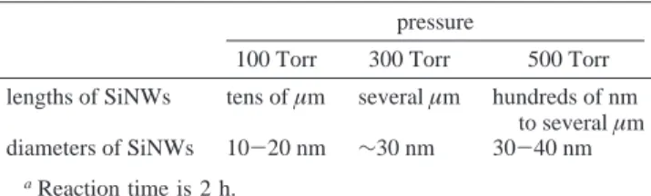
3.3. Pressure Effect. To study the size dependence of SiNWs on reacting pressure, three pressure sets of Ar carrier gas, 100, 300, and 500 Torr, have been selected in the synthesis of SiNWs
from Si + SiO2 + Pr6O11. Most of the fabricated nanowires
become shorter and wider with increasing Ar carrier pressure as listed in Table 2, indicating while the longitudinal (lengths of SiNWs) growing rate decreases with increasing pressure, the transversal (diameters of SiNWs) one increases.
If under the VLS mechanism, the size of initially formed nanoclusters/nanoparticles is responsible for the diameter of
nanowires, such as the FeSi2liquid-droplet in the Fe-catalytic
synthesis of SiNWs. The relation between the diameter of nanoclusters d and the ambient gas pressure p is governed by
the inertia fluid model of Yoshida et al.,47
From Yoshida’s experimental results, they found n ) 1/2.8 for
the production of Si nanoparticles by laser ablation with ambient He gas flowing at a constant pressure. Following this model,
Zhang et al.33also gave similar Ar pressure effect (n ) 1/2.5)
on the growth of SiNWs. Taking our results listed in Table 2 and fitting into eq 2, the dependence (n ) 1/1.72) of the diameter of SiNWs on the ambient Ar pressure has been determined.
Possible reasons could be found to explain the deviation of our abnormally large n ) 1/1.72 value from the inertia fluid
model by Yoshida et al.47 First, SiO2, rather than the metal
catalyst, plays a dominant catalytic role in our experiment for
the fabrication of SiNWs from Si + SiO2+ Pr6O11as discussed
in the preceding section. The deviation could stem from a reaction process not complying with the VLS mechanism. Second, a gas-flowing system was employed in our experiment. At higher ambient Ar carrier-gas pressure, the initially formed nanoclusters of Si-grain on SiO2-substrate are subject to more collisions with Ar atoms, thus slowing down the average drift-velocity of the nanoclusters. Accordingly, the traveling of the nanoclusters takes longer time before their landing on the copper coldfinger or the Si collection-substrate. During this longer period of flight time, bigger sizes of nanoclusters possibly grow, and wider SiNWs are produced consequently.
Meanwhile, the vaporization rate of Si was kept constant under the laser ablation. The absorption/adsorption rate of Si vapor on the nanoclusters of Si-grain on SiO2-substrate should roughly maintain the same. In a fixed period of time with a constant Si vapor supply, if the SiNW becomes wider, a shorter length of the fabricated SiNW is resulted.
4. Conclusion
We have investigated the growths of crystalline SiNWs with
the catalyses of pure metals (Fe, Ru, and Pr) and SiO2. Si{111}
planes have been found to be most stable in these catalytic
fabrications. While the wire growth axis is along〈111〉for the
metal-catalytic SiNWs complying with VLS mechanism, the
wire growth axis directs to〈112〉in the SiNWs catalyzed by
SiO2. Different growth mechanisms for metal- and SiO2-catalytic syntheses of SiNWs have been discussed. Pressure effect on the growing process has been examined. Possible reasons have been provided to explain the observations.
Acknowledgment. The SEM, TEM, HRTEM, ED, SAED, and EDS measurements for this study in Instrumentation Center of National Taiwan University and Instrumentation Center of National Tsing-Hua University, both sponsored by National Science Council of ROC, are acknowledged. This work is supported by CTCI Foundation and National Science Council of ROC (Grant Nos. 91-2113-M-002-035 and 91-2120-M-002-001).
References and Notes
(1) Alivisatos, A. P. Science 1996, 271, 933.
(2) Baron, T.; Martin, F.; Mur, P.; Wyon, C.; Dupuy, M.; Busseret, C.; Souifi, A.; Guillot, G. Appl. Surf. Sci. 2000, 164, 29.
Si + SiO2f 2SiO (1a)
2SiO f 2SiOx+ (1 - x)O2 (1b)
SiOxf Si1-x+ x(SiO) (1c)
2SiO f Si + SiO2 (1d)
d∞pn, n )1
3 (2)
TABLE 2: Size Dependence of SiNWs on the Pressure of Ar Carrier Gasa
pressure
100 Torr 300 Torr 500 Torr lengths of SiNWs tens ofµm severalµm hundreds of nm
to severalµm diameters of SiNWs 10-20 nm ∼30 nm 30-40 nm
aReaction time is 2 h.
Downloaded by NATIONAL TAIWAN UNIV on September 3, 2009 | http://pubs.acs.org
(3) Park, N.-M.; Kim, S. H.; Sung, G. Y.; Park, S.-J. Chem. Vap. Deposition 2000, 8, 254.
(4) Liu, H. I.; Biegeisen, D. K.; Ponce, F. A.; Johnson, N. M.; Pease, R. F. W. Appl. Phys. Lett. 1994, 64, 1383.
(5) Wakayama, Y.; Tanaka, S. J. Cryst. Growth 1997, 181, 304. (6) Ono, T.; Saitoh, H.; Esashi, M. Appl. Phys. Lett. 1997, 70, 1852. (7) Sanders, G. D.; Chang, Y. C. Phys. ReV. B 1992, 45, 9202. (8) Wang, N.; Zhang, Y. F.; Tang, Y. H.; Lee, C. S.; Lee, S. T. Appl. Phys. Lett. 1998, 73, 3902.
(9) Wang, N.; Tang, Y. H.; Zhang, Y. F.; Lee, C. S.; Lee, S. T. Phys. ReV. B 1998, 58, 16024.
(10) Wang, N.; Tang, Y. H.; Zhang, Y. F.; Lee, C. S.; Bello, I.; Lee, S. T. Chem. Phys. Lett. 1999, 299, 237.
(11) Tang, Y. H.; Zheng, Y. F.; Lee, C. S.; Lee, S. T. Chem. Phys. Lett.
2000, 328, 346.
(12) Zhang, Y. F.; Tang, Y. H.; Wang, N.; Yu, D. P.; Lee, C. S.; Bello, I.; Lee, S. T. Appl. Phys. Lett. 1998, 72, 1835.
(13) Wang, N.; Tang, Y. H.; Zhang, Y. F.; Yu, D. P.; Lee, C. S.; Bello, I.; Lee, S. T. Chem. Phys. Lett. 1998, 283, 368.
(14) Zhang, Y. F.; Tang, Y. H.; Wang, N.; Lee, C. S.; Bello, I.; Lee, S. T. J. Cryst. Growth 1999, 197, 136.
(15) Tang, Y. H.; Zhang, Y. F.; Wang, N.; Shi, W. S.; Lee, C. S.; Bello, I.; Lee, S. T. J. Vac. Sci. Technol. B 2001, 19, 317.
(16) Lee, S. T.; Zhang, Y. F.; Wang, N.; Tang, Y. H.; Bello, I.; Lee, C. S.; Chung, Y. W. J. Mater. Res. 1999, 14, 4503.
(17) Fan, X. H.; Xu, L.; Li, C. P.; Zheng, Y. F.; Lee, C. S.; Lee, S. T. Chem. Phys. Lett. 2001, 334, 229.
(18) Shi, W. S.; Peng, H. Y.; Zheng, Y. F.; Wang, N.; Shang, N. G.; Pan, Z. W.; Lee, C. S.; Lee, S. T. AdV. Mater. 2000, 12, 1343.
(19) Zhang, Y. F.; Tang, Y. H.; Lam, C.; Wang, N.; Lee, C. S.; Bello, I.; Lee, S. T. J. Cryst. Growth 2000, 212, 115.
(20) Li, C. P.; Sun, X. H.; Wong, N. B.; Lee, C. S.; Lee, S. T.; Teo, B. K. Chem. Phys. Lett. 2002, 365, 22.
(21) Morales, A. M.; Lieber, C. M. Science 1998, 279, 208. (22) Hu, J.; Odom, T. W.; Lieber, C. M. Acc. Chem. Res. 1999, 32, 435.
(23) Duan, X.; Lieber, C. M. J. Am. Chem. Soc. 2000, 122, 188. (24) Cui, Y.; Leiber, C. M. Science 2001, 291, 851.
(25) Hu, J.; Ouyang, M.; Yang, P.; Lieber, C. M. Nature 1999, 399, 48.
(26) Cui, Y.; Lauhon, L. J.; Gudiksen, M. S.; Wang, J.; Lieber, C. M. Appl. Phys. Lett. 2001, 78, 2214.
(27) Yu, D. P.; Lee, C. S.; Bello, I.; Sun, X. S.; Tang, Y. H.; Zhou, G. W.; Bai, Z. G.; Feng, S. Q. Solid State Commun. 1998, 105, 403.
(28) Yu, D. P.; Bai, Z. G.; Ding, Y.; Hang, Q. L.; Zhang, H. Z.; Wang, J. J.; Zou, Y. H.; Qian, W.; Xiong, G. C.; Zhou, H. T.; Feng, S. Q. Appl. Phys. Lett. 1998, 72, 3458.
(29) Feng, S. Q.; Yu, D. P.; Zhang, H. Z.; Bai, Z. G.; Ding, Y. J. Cryst. Growth 2000, 209, 513.
(30) Zhou, G.; Zhang, Z.; Yu, D. P. J. Cryst. Growth 1999, 197, 129. (31) Yu, D. P.; Bai, Z. G.; Wang, J. J.; Zou, Y. H.; Qian, W.; Fu, J. S.; Zhang, H. Z.; Ding, Y.; Xiong, G. C.; You, L. P.; Xu, J.; Feng, S. Q. Phys. ReV. B 1999, 59, 2498.
(32) Zhou, G. W.; Zhang, Z.; Bai, Z. G.; Feng, S. Q.; Yu, D. P. Appl. Phys. Lett. 1998, 73, 677.
(33) Zhang, H. Z.; Yu, D. P.; Ding, Y.; Bai, Z. G.; Hang, Q. L.; Feng, S. Q. Appl. Phys. Lett. 1998, 73, 3396.
(34) Bai, Z. G.; Yu, D. P.; Wang, J. J.; Zou, Y. H.; Qian, W.; Fu, J. S.; Feng, S. Q.; Xu, J.; Lou, L. P. Mater. Sci. Eng. B 2000, 72, 117.
(35) Xing, Y. J.; Yu, D. P.; Xi, Z. H.; Xue, Z. Q. Chin. Phys. 2002, 11, 1047.
(36) Xing, Y. J.; Xi, Z. H.; Yu, D. P.; Hang, Q. L.; Yan, H. F.; Feng, S. Q.; Xue, Z. Q. Chin. Phys. Lett. 2002, 19, 240.
(37) Yan, H. F.; Xing, Y. J.; Hang, Q. L.; Yu, D. P.; Wang, Y. P.; Xu, J.; Xi, Z. H.; Feng, S. Q. Chem. Phys. Lett. 2000, 323, 224.
(38) Wagner, R. S.; Ellis W. C. Appl. Phys. Lett. 1964, 4, 89. (39) In Whisker Technology; Levitt, A. P., Ed.; Wiley-Interscience: New York, 1970; pp 47-119.
(40) Seddon, E. A.; Seddon, K. R. The Chemistry of Ruthenium; Elsevier: Amsterdam, 1984.
(41) Harris, D. C. QuantitatiVe Chemical Analysis, 4th ed.; W. H. Freeman and Company: New York, 1995.
(42) Ishida, S.; Iwamoto, Y.; Kabuto, C.; Kira, M. Nature 2003, 421, 725.
(43) Ma, X. L.; Zhu, Y. L.; Zhang, Z. Philos. Mag. Lett. 2002, 82, 461. (44) Boehm, H. P. Carbon 1973, 11, 583.
(45) Dimitriadis, C. A.; Stoemenos, J.; Coxon, P. A.; Friligkos, S.; Antonopoulos, J.; Economou, N. A. J. Appl. Phys. 1993, 73, 8402.
(46) In Silicon-Based Materials and DeVices; Nalwa, H. S., Ed.; Academic Press: San Diego, 2001; Vol. 2, pp 193-223.
(47) Yoshida, T.; Takeyama, S.; Yamada, Y.; Mutoh, K. Appl. Phys. Lett. 1996, 68, 1772.
Downloaded by NATIONAL TAIWAN UNIV on September 3, 2009 | http://pubs.acs.org