國
立
交
通
大
學
電子工程學系 電子研究所
博 士 論 文
應用於多核心系統晶片之節能晶內資料傳輸
-以記憶儲存為重心
Energy-Efficient Memory-Centric On-Chip Data
Communication for Multi-Core SoCs
研 究 生:黃 柏 蒼
指導教授:黃 威 教授
應用於多核心系統晶片之節能晶內資料傳輸
-以記憶儲存為重心
Energy-Efficient Memory-Centric On-Chip Data
Communication for Multi-Core SoCs
研 究 生:黃 柏 蒼 Student:Po-Tsang Huang
指導教授:黃 威 教授 Advisor:Prof. Wei Hwang
國 立 交 通 大 學
電 子 工 程 學 系 電 子 研 究 所
博 士 論 文
A Dissertation
Submitted to Department of Electronics Engineering and Institute of Electronics
College of Electrical and Computer Engineering National Chiao Tung University
in partial Fulfillment of the Requirements for the Degree of
Doctor of Philosophy in
Electronics Engineering November 2010
Hsinchu, Taiwan, Republic of China
應用於多核心系統晶片之節能晶內資料傳輸
-以記憶儲存為重心
學生:黃 柏 蒼 指導教授:黃 威 教授
國立交通大學電子工程學系電子研究所
摘 要
隨著人們對於無所不在的無線高速資料傳輸多媒體影音需求逐年增加,多 核心系統晶片要能有效地提供大量的資料運算、資料傳輸以及資料儲存才有辦法 達到未來的系統需求。在本論文中,我們提出了適合於異質多核心系統晶片之晶 內資料傳輸平台-以記憶儲存為重心之節能晶內資料傳輸平台,此平台由兩部分 構 成 , 分 別 為 以 記 憶 體 為 重 心 之 晶 內 連 線 網 路(memory-centric on-chipinterconnection network)以及隨隨記憶體子系統(on-demand memory sub-system)。 此平台提供足夠的資料傳輸頻寬、記憶體存取頻寬以及記憶儲容量,並將其應用 在無線影像娛樂系統上。 以記憶體為重心之晶內連線網路提供微架構及構成要素給晶內資料傳輸平 台,構成要素包括了路由器(router)、連接導線(link wires)及網路介面(network interface)。在連接導線部分,我們提出了具能源效應及可靠度頻道設計,利用自 我修正節能編碼及自我補償電壓調整技術,能有效地減少導線間的耦合效應,並 且提供頻道錯誤更正及電壓調整機制。在路由器方面,我們設計了兩階層先進先 出資料暫存器,藉由提升集中式資料暫存器的使用率及降低線頭阻塞來提升晶內 網路效能。為了更進一步的提升網路效能,我們也提出了具堵塞感知之適應性路 由演算法,藉由偵測路由器附近的資料傳輸情況,可以避開雍塞的路線。此外,
我們提出了具能源效益的路由表設計給晶內連線網路及IPv6使用,此路由表是由 高速且低功率三元定址記憶體(TCAM)陣列構成,其中包含了互斥或邏輯閘的條 件式維持器、蝴蝶式比較線連接、階層式搜尋線及電源截段技術。 隨選記憶體子系統負責有效地管理異質多核心系統晶片中多執行程序的記 憶體存取,讓系統達到最佳的記憶體使用率。在所提出的隨選記憶體子系統中, 主要包含了私有式記憶體管理器以及集中式記憶體管理器。在私有式記憶體管理 器中,主要是負責控制第一層快取(L1 cache)存取;此外,我們也提出了一個借 取機制,此機制可以動態地分配快取中的記憶體資源給晶內網路封包的暫存使 用,以減少處理單元暫停的情況。而在集中式記憶體管理器中,主要是負責管理 第二層快取(L2 cache)及外部記憶體之資料存取,利用所提出的適應性快取控制 機制,我們可以根據不同處理單元的記憶體存取需求,動態地分配所需記憶體資 源。此外,在集中式記憶體管理器中也建構了一個外部記憶體存取介面來有效地 存取晶片外的動態記憶體(DRAM)。另外,針對應用於無線影像娛樂系統上的可 階式視訊編碼(scalable video coding),我們提出了跨層間預取資料(inter-layer pre-fetch)機制和有效率的動態記憶體位址轉換器來減少快取記憶體的失誤率以 及記憶體的能源消耗。
Energy-Efficient Memory-Centric On-Chip Data
Communication for Multi-Core SoCs
Student : Po-Tsang Huang Advisors : Prof. Wei Hwang
Department of Electronics Engineering & Institute of Electronics
National Chiao-Tung University
ABSTRACT
With increasing demands on ubiquitous wireless high-data-rate multimedia services, it is critical to have efficient capabilities of the data processing, data communication and data storage to sustain the growth in multi-core system-on-chips (SoCs). In this dissertation, an energy-efficient memory-centric on-chip data communication platform, consisting of a memory-centric on-chip interconnection network (OCIN) and an on-demand memory sub-system, is proposed to provide enough data communication bandwidth, memory bandwidth and memory capacity for heterogeneous multi-core SoCs in wireless video entertainment systems.
The memory-centric OCIN provides the micro-architecture and building blocks, including routers, link wires and network interfaces (NIs), for the on-chip data communication platform. Therefore, an energy-efficient and reliable channel desgn is presented via a self-corrected green coding scheme and a self-celibrated voltage scaling technique to reduce the couping effects of link wires and provide the error correction and voltage scaling mechanisms. Conseuqently, a two-level FIFO buffer router is proposed to enhance the on-chip network performance by increasing the utility of the centralized buffer and reducing the head-of-line blocking problems. Accordingly, an adaptive congestion-aware routing algorithm is also proposed to further increase the performance of mesh networks by detecting the traffic around a routing node. Moreover, energy-efficient routing tables are presented for OCINs and IPv6 applications via the high-performance and low-power ternary content addressable memory (TCAM), which is desinged by noise-tolerant XOR-based
conditional keepers, butterfly match-lines, don’t-care-based hierarchical search-lines and don’t-care-based power gating.
The on-demand memory sub-system is presented to efficiently manage memory accesses of multi tasks in heterogeneous multi-core SoCs via private memory management units (p-MMUs) and a centralized MMU (c-MMU). The p-MMUs control data accesses of L1 caches and dynamically allocate memory resources for network data buffering to reduce the stall of processor elements (PEs) based on the proposed borrowing mechanism. Furthermore, the c-MMU manages centralized on-chip memories (L2 cache) and off-chip memories. For different memory requirements of the PEs in multi tasks, adaptive memory resource allocation is realized to increasing the ovaerall performance using the proposed adaptive cache control. Additionally, an external memory interface (EMI) is develpoed in the c-MMU to access the off-chip DRAM efficiently. Furthermore, an inter-layer pre-fetch mechanism and an efficient address translator are proposed to reduce both the cache miss rate and memory energy consumption for scalable video coding (SVC) in the wireless video entertainment system.
Acknowledgements
我要感謝我的指導教授黃威教授這幾年對我的指導和鼓勵,在研究過程中提 供了很多方向和指引,才讓我的研究可以順利完成。特別感謝老師能讓我同時學 習到記憶體設計、記憶體系統、晶內資料傳輸及多媒體與系統整合的領域,使我 的研究雖然辛苦但是充滿了挑戰及樂趣。另外要感謝就是跟我同一個團隊的博士 班同學和學弟們,使我在研究的過程中激盪出許多想法,也在我研究所的生活 中,增添了許多的樂趣。在我的研究過程幫助了我很多也教導了我很多,從他們 身上得到很多寶貴的建議。特別感謝eHome 計畫團隊的黃威教授、黃經堯教授、 闕河鳴教授、張錫嘉教授、張添烜教授、許騰尹教授、劉志尉教授、桑梓賢教授、 陳宏明教授及黃俊達教授的指導,使我有系統整合的機會與經驗。在團隊工作期 間,與各個子計畫的同學也互有往來,感謝各位同學的配合與指教,更提供了很 多不同的方向的建議。 最後要感謝我的家人、幼幼社多年來的夥伴及電子系的家族學弟妹們,在研 究過程給我的打氣與鼓勵以及關心,並陪伴我渡過許多的挫折及難關,讓我的研 究過程能順利完成。Contents
Chapter 1: Introduction ... 1
1.1 Motivation... 2
1.2 Contributions of This Dissertation ... 7
1.2.1 Link Wires ... 8
1.2.2 Routers ... 8
1.2.3 Network Interfaces ... 10
1.2.4 On-Demand Memory Sub-system ... 10
1.3 Organization of This Dissertation ... 11
Chapter 2: Survey of On-Chip Data Communication ... 14
2.1 Why NoC and OCIN? ... 15
2.2 Design Abstraction Levels of NoC ... 18
2.3 Network Topologies of OCINs ... 22
2.4 Flow Control and Switching Technique for OCINs ... 27
2.4.1 Packet-Buffer Flow Control ... 29
2.4.2 Flit-Buffer Flow Control ... 30
2.4.3 Buffer Management and Backpressure ... 32
2.5 Link Wires for OCINs ... 34
2.6 Routers for OCINs ... 39
2.6.1 Routing Algorithm for Link Control ... 40
2.6.2 Switching Matrix (Crossbar) in Routers ... 45
2.6.3 Arbitration Unit in Routers ... 46
2.6.4 Queuing Buffer in Routers ... 46
2.7 Network Interfaces (NIs) for OCINs ... 47
2.8 Power Analysis for NoCs ... 49
2.9 Power Management for NoCs ... 51
2.10 Memory is Network!!! ... 57
2.10.1 Cache Partition Methods ... 59
2.10.2 Data Consistency in Reconfigurable Cache ... 62
2.10.3 Reconfiguration Policy and Detection ... 63
2.11 Summary ... 64
Chapter 3: Energy-Efficient and Reliable Channels for OCINs
... 66
3.1 Background ... 66
3.2 Self-Calibrated Low Power and Energy-Efficient Channel Design ... 70
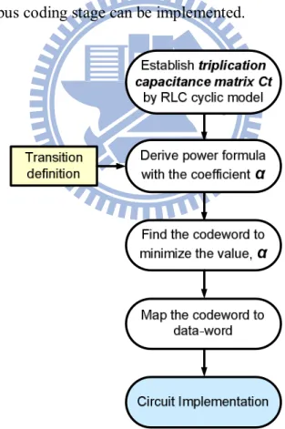
3.3 Self-Corrected Green (SGC) Coding Scheme ... 72
3.3.1 Triplication Error Correction Stage ... 72
3.3.2 Joint Triplication Bus Power Model ... 76
3.3.3 Green Bus Coding Stage for Crosstalk Avoidance ... 80
3.4 Self-Calibrated Voltage Scaling Technique ... 83
3.4.1. Crosstalk-Aware Test Error Detection Stage... 86
3.4.2. Run-Time Error Detection Stage ... 88
3.5 Simulation Results ... 92
3.6 Summary ...103
Chapter 4: Two-Level FIFO Buffer Design for Routers ... 105
4.1 Background ...105
4.2 Buffer Implementations and Architectures ...108
4.3 Concept of Two-Level FIFO Buffer Scheme... 113
4.4 Synchronous Two-Level FIFO Buffer Architecture ... 117
4.4.1 Header Decoder and Routing ... 118
4.4.2 Data-Link Scheduler and Centralized Level-2 FIFO ... 118
4.4.3 Distributed level-1 FIFO ...121
4.4.4 Arbiter ...121
4.5 Asynchronous Two-Level FIFO Buffer Architecture...122
4.6 Associated Two-Level FIFO Buffer Architecture ...127
4.7 Simulation Results ...128
4.7.1 Synchronous Two-Level FIFO Buffer ...128
4.7.2 Asynchronous Two-Level FIFO Buffer ...137
4.8 Summary ...139
Chapter 5: Adaptive Congestion-Aware Routing Algorithm for
Mesh On-Chip Interconnection Networks ... 141
5.1 Background ...141
5.2 Congestion-Aware Routing Concept ...144
5.3 Congestion-Aware Routing Algorithm ...147
5.3.1 Deadlock Avoidance by the Odd-Even Turn Model ...147
5.3.2 Score Calculator ...148
5.3.3 Adaptive Decision Unit ...150
5.4 QoS Guarantee Arbitration Mechanism ...151
5.5 QoS Guarantee Arbitration Mechanism ...153
5.6 Summary ...158
Chapter 6: Energy-efficient Routing Tables for OCINs and
IPv6 Applications ... 160
6.1 Background ...160
6.2 Routing Tables in OCINs...162
6.3 Architecture of TCAM Macro in Network Routers ...164
6.4 Energy-Efficient Match-Line ...167
6.4.1 Butterfly Match-line Scheme ...168
6.4.2 XOR-based Conditional Keeper for Match-Line ...171
6.5 Don’t-Care Based Hierarchy Search-Line Scheme ...174
6.6 Don’t-Care Based Hierarchy Power Gating Techniques ...177
6.6.1 Multi-Mode Data-Retention Power Gating ...178
6.6.2 Super Cut-Off Power Gating ...181
6.7 TCAM Macro Implementation and Measurements ...186
6.8 Summary ...195
Chapter 7: On-Demand Memory Sub-system for Multi-Task
Wireless Video Entertainment Systems ... 197
7.1 Background ...198
7.2 Wireless Video Entertainment System ...202
7.2.1 Wireless Processing Unit (WPU) ...205
7.2.2 Medium Access Control (MAC) ...206
7.2.3 Luby-Transform (LT) Coding ...208
7.2.4 Scalable Video Coding (SVC)...210
7.3 Architecture of On-Demand Memory Sub-System...212
7.4 Private Memory Management Unit (p-MMU) ...216
7.4.1 Buffer Borrowing Mechanism ...217
7.4.2 Borrowing Address Generator...218
7.4.3 Buffering Control ...220
7.4.4 Simulation Results of Buffer Borrowing Mechanism ...222
7.5 Centralized Memory Management Unit (c-MMU) ...222
7.5.1 Adaptive Cache Controller ...224
7.6 Pre-fetch Mechanism and Address Translator for SVC ...235
7.6.1 Inter-Layer Pre-Fetch Scheme ...235
7.6.2 Address Translator for SVC ...241
7.7 Analysis of On-Demand Memory Sub-System ...245
7.8 Summary ...256
Chapter 8: Conclusions and Future Works ... 259
8.1 Conclusions ...259 8.2 Futures Works ...261
Bibliography ... 263
References of Chapter 1 ...263 References of Chapter 2 ...264 References of Chapter 3 ...280 References of Chapter 4 ...283 References of Chapter 5 ...287 References of Chapter 6 ...288 References of Chapter 7 ...292Vita ... 296
List of Figures
Chapter 1
Fig. 1.1 A heterogeneous network environment for wireless video entertainment
systems. ... 1
Fig. 1.2 Vertical exploration of a multi-core system. [1.14] ... 4
Fig. 1.3 Comparison between memory bandwidth, computation capability and communication efficiency in multi-core SoCs. ... 5
Fig. 1.4 Relative complexity of a video system. [1.15] ... 5
Fig. 1.5 Energy-efficient on-chip data communication platform with a memory-centric OCIN and an on-demand memory sub-system. ... 6
Fig. 1.6 The contribution matrix of energy-efficient memory-centric on-chip data communication ... 7
Chapter 2
Fig. 2.1 The organization of Chapter 2. ... 15Fig. 2.2 A conventional on-chip bus platform. [2.10] ... 15
Fig. 2.3 Multi-layer bus architecture. [2.24] ... 17
Fig. 2.4 On-chip interconnection network, including routers, link wires and network interfaces. [2.9] ... 18
Fig. 2.5 The design abstraction layers of NoC [2.27] ... 19
Fig. 2.6 The reduced NoC protocol stack. [2.29] ... 19
Fig. 2.7 Data abstraction. [2.7] ... 21
Fig. 2.8 NoC research areas versus OSI model based on the flow of data. [2.31] .. 21
Fig. 2.9 NoC Research category based on design abstraction layers and flow of data abstraction. [2.31] ... 22
Fig. 2.10 Conventional network topologies of OCIN (a) SPIN (b) Mesh (c) Torus (d) Folded tours (e) Octagon (f) Butterfly Fat tree. [2.35] ... 23
Fig. 2. 11 Xipies Architecture. [2.42] ... 24
Fig. 2.12 A Hierarchical OCIN architecture. [2.43] ... 25
Fig. 2.13 (a) Energy consumption (b) network area according to a number of PEs. [2.48] ... 26
Fig. 2.14 Buffered flow control methods can be classified based on their granularity of channel bandwidth allocation and buffer allocation. [2.54] ... 28
Fig. 2.15 Virtual channels. [2.8] ... 31
Fig. 2.16 A robust self-calibrating transmission scheme for OCIN links. [2.62] .... 34
Fig. 2.18 Implementation of boundary-shift codes (BSC). [2.72] ... 37
Fig. 2.19 A unified coding framework for link wires. [2.71] ... 37
Fig. 2.20 A bi-direction channels to optimize the utilization of link wires. [2.74] . 38 Fig. 2.21 Lookahead-based adaptive voltage scheme. [2.77] ... 39
Fig. 2.22 Micro-architecture of a router for mesh-based OCINs. [2.9]... 40
Fig. 2.23 A category of Routing Algorithms Grouping. [2.91] ... 41
Fig. 2.24 An example of deadlock. [2.92] ... 42
Fig. 2.25 A dynamic routing algorithm for avoiding hot spots. [2.90] ... 43
Fig. 2.26 Example for neighbors-on-path algorithm. [2.94] ... 44
Fig. 2.27 Crossbar partial activation technique. [2.48] ... 46
Fig. 2.28 Network interfaces connecting cores to the NoC and possible message dependencies in (a) shared-memory and (b) message-passing communication paradigms. [2.121] ... 48
Fig. 2.29 Block diagram of network interface supporting the CTC protocol. [2.121] ... 48
Fig. 2.30 Four levels for power analysis of OCINs... 50
Fig. 2.31 Power model database development flow in system. [2.131] ... 51
Fig. 2.32 Design Flow of NoC Synthesis. [2.134] ... 51
Fig. 2.33 A methodology for managing power consumption of NOCs via the estimator. [2.136] ... 52
Fig. 2.34 Point-to-point GALS architecture. [2.142] ... 53
Fig. 2.35 GALS systems based on plausible clocking. [2.143] ... 54
Fig. 2.36 GALS systems based on clock gating. [2.143] ... 54
Fig. 2.37 Locally delayed latching (LDL) synchronization. [2.145] ... 55
Fig. 2.38 Bypass architecture of the self-timed ring. [2.154] ... 56
Fig. 2.39 Architecture of GALS NoC unit in a voltage island. [2.157] ... 57
Fig. 2.40 Memory is network. [2.161] ... 58
Fig. 2.41 Associativity-based partitioning organization for reconfigurable caches. [2.165] ... 59
Fig. 2.42 A selective-ways organization and a selective-sets organization. [2.169] 60 Fig. 2.43 Cache access method in Molecules. [2.171] ... 61
Fig. 2.44 An example of typical CMP cache partitioning. [2.172] ... 62
Chapter 3
Fig. 3.1 A unified framework for joint crosstalk avoidance code and error correction code. ... 68 Fig. 3.2 Self-calibrated energy-efficient and reliable channels for on-chipand self-calibrated voltage scaling technique. ... 70
Fig. 3.3 Triplication error correction stage of SCG coding scheme. ... 72
Fig. 3.4 The corresponding voltages of specific error correction coding versus different un-coded word-error- rate with (a) k = 8 (b) k = 32. ... 76
Fig. 3.5 (a) Bus Model for 4 bits (b) The approximate bus power model. ... 77
Fig. 3.6 Five transition types for two adjacent wires. ... 78
Fig. 3.7 The design flow of the green bus coding stage. ... 80
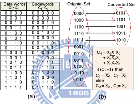
Fig. 3.8 (a) The mapping table between 4-bit dataword and 5-bit codeword of the green bus coding stage (b) The two sets and Boolean expression of the green bus coding stage... 81
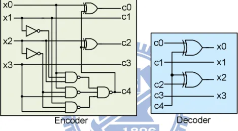
Fig. 3.9 The encoder and decoder of green bus coding stage. ... 82
Fig. 3.10 The block diagrams of self-calibrated voltage scaling technique with crosstalk-aware test error detection stage and run-time error detection stage. 83 Fig. 3.11 (a) Low swing voltages (b) Low swing driver (c) Level converter. ... 85
Fig. 3.12 The control policy of self-calibrated voltage scaling technique. ... 85
Fig. 3.13 MAF based test pattern generator (a) 8 states complete 6 faults test of MAF model (b) Hardware implementation. ... 87
Fig.3.14 Modified double sampling data checking circuit and Wwaveforms (a) error-free (b) delay error (c) glitch error. ... 90
Fig. 3.15 The energy-delay product (EDP) reduction to un-coded code under different values of λ with (a) full swing signal (b) the lowest swing signal. .. 95
Fig. 3.16 Simulation environment setup with different number of routers (N) and different lengths (M) of link wires. ... 96
Fig. 3.17 Energy reduction under different lengths of link wires and different number of routers. ... 97
Fig. 3.18 Energy dissipation of an 8x8 mesh-NoC with different joint CAC and ECC coding schemes. ... 97
Fig. 3.19 The data path delay(td) distributions of rising speed-up, falling speed-up, rising delay, falling delay, normal rising and normal falling cases under (a) high voltage (1.0v) (b) medium voltage (0.85v) (c) low voltage (0.7v). ... 99
Fig. 3.20 Voltage levels of the self-calibrated voltage scaling technique under six phases with different noise distributions and timing variations. ...100
Fig. 3.21 Energy analysis of the self-calibrated energy-efficient and reliable interconnection architecture. ...101
Chapter 4
Fig. 4.1 A generic router architecture. ...106Fig. 4.3 Head-of-line blocking problem induced by insufficient buffer. ...108
Fig. 4.4 Different buffer implementation (a) Shift Register (b) Bus-In Shift-Out Register (c) Bus-In Bus-Out Register (d) Bus-In MUX-Out Register. ...109
Fig. 4.5 Diagram of input buffer, middle buffer and output buffer. ... 111
Fig. 4.6 Concepts of (a) dynamic virtual channel allocation (b) centralized shared buffer. ... 112
Fig. 4.7 Data flow of two-level FIFO buffer scheme. ... 114
Fig. 4.8 Concept of the data-link-based FIFO. ... 115
Fig. 4.9 An example of two-level FIFO buffer scheme. ... 116
Fig. 4.10 Two-level FIFO buffer architecture in routers. ... 117
Fig. 4.11 Data-linked based centralized level-2 FIFO and data-link scheduler. .... 119
Fig. 4.12 Implementation of the centralized level-2 FIFO. ...120
Fig. 4.13 Example of the arbitration policy in deterministic routing algorithms. ..122
Fig. 4.14 Asynchronous two-level FIFO buffer architecture. ...123
Fig. 4.15 Data-link scheduler and centralized level-2 FIFO for asynchronous two-level FIFO buffer. ...125
Fig. 4.16 STG specification for the read operation and write operation of the centralized level-2 FIFO. ...126
Fig. 4.17 Different associations between the distributed level-1 FIFO and the centralized level-2 FIFO for 8 output channels. ...127
Fig. 4.18 Pipeline stages of the generic router, DSB router and two-level FIFO buffer router. ...129
Fig. 4.19 Normalized performance versus FIFO sizes with different buffer organizations in (a) low injection load (b) medium injection load (c) high injection load. ...130
Fig. 4.20 Average latencies of different buffer architectures in (a) uniform patterns (b) hotspot patterns. ...132
Fig. 4.21 Average latencies of XY, DyXY and adaptive routing algorithms in (a) uniform patterns (b) hotspot patterns. ...133
Fig. 4.22 Power and area analysis of the different associated two-level FIFO buffers in an 8input/8output router. ...136
Fig. 4.23 The demonstrated 8x8 DCT system for an asynchronous router...137
Fig. 4.24 Latencies, area and energy dissipations for an 8x8 DCT with different buffers. ...138
Chapter 5
Fig. 5.1 The architecture of the congestion-aware router. ...144Fig. 5.3 The architecture of adaptive congestion-aware routing algorithm. ...147
Fig. 5.4 An example of the score calculation ...148
Fig. 5.5 An example of the adaptive decision. ...150
Fig. 5.6 QoS guarantee arbitrator. ...152
Fig. 5.7 The average latencies versus the specific switching values under the uniform patterns (a) without hotspots (b) with 6 hotspots. ...153
Fig. 5.8 Hotspots setting for the 8x8 mesh network. ...154
Fig. 5.9 The average latencies versus the specific switching values under the transpose patterns (a) without hotspots (b) with 6 hotspots. ...155
Fig. 5.10 The comparisons under the uniform patterns (a) without hotspots (b) with 6 hot spots. ...156
Fig. 5.11 The comparisons under the transpose patterns. ...157
Chapter 6
Fig. 6.1 Binary CAM (BCAM) cell and ternary CAM (TCAM) cell. ...161Fig. 6.2 A routing table organized with source routes. ...163
Fig. 6.3 A simplified block diagram of a TCAM macro and packet forwarding by an address-lookup table in network routers...164
Fig. 6.4 PF-CDPD And-type match-line scheme. ...166
Fig. 6.5 Transfer dynamic logic into clock-and-data pre-charge dynamic (CDPD) circuits. ...166
Fig. 6.6 Butterfly match-line scheme. ...168
Fig. 6.7 AND-type match-line with XOR-based conditional keeper. ...171
Fig. 6.8 (a) Search time (b) Power consumption versus UNG margin for different keepers. ...172
Fig. 6.9 Butterfly connection style with XOR-based conditional keeper and don’t-care based power gating scheme. ...174
Fig. 6.10 Packet routing based on longest prefix matching mechanism. ...175
Fig. 6.11 (a) A simplified architecture (b) Circuit implementation of don’t-care based hierarchical search-line scheme. ...175
Fig. 6.12 Timing analysis of don’t-care based hierarchical search-line scheme. ...177
Fig. 6.13 The architecture of super cut-off power gating and multi-mode data-retention power gating techniques. ...178
Fig. 6.14 Multi-mode data-retention power gating technique. ...179
Fig. 6.15 Relation between noise margin, leakage saving and scale factor. ...180
Fig. 6.16 Super cut-off power gating technique. ...181
Fig. 6.17 Control circuits for (a) PMOS (b) NMOS cut-off switch. ...183 Fig. 6.18 (a) VBB generator (b) Voltage doubler for super cut-off power gating. .184
Fig. 6.19 Analysis of voltage generators for different number of match-lines. ...185
Fig. 6.20 Analysis of the search time under different energy-efficient schemes. ..186
Fig. 6.21 Analysis of the energy consumption under different energy-efficient schemes. ...187
Fig. 6.22 Standby power analysis under different power gating techniques. ...188
Fig. 6.23 Search time of one stage under 3σ process variations. ...188
Fig. 6.24 Layout view of 1-bit TCAM cell and a TCAM segment with 6-bit TCAM cells. ...189
Fig. 6.25 Layout view of 256x144 TCAM array and test chip micrograph. ...191
Fig. 6.26 Measurement setup. ...191
Fig. 6.27 (a) Block diagram of the test chip (b) Test strategy. ...192
Fig. 6.28 Energy consumption under different don’t care patterns. ...193
Fig. 6.29 Network address prefix distribution of IPv6. ...193
Fig. 6.30 Average standby power with different power gating modes. ...195
Chapter 7
Fig. 7.1 Memory hierarchy. ...198Fig. 7.2 Simplified architecture of a DRAM. ...200
Fig. 7.3 Configurations of different layers of the proposed memory controller. ...201
Fig. 7.4 Multi-Task wireless video entertainment system. ...203
Fig. 7.5 Block diagram of the wireless video entertainment system. ...204
Fig. 7.6 Single-FFT Architecture for MIMO Modem. ...205
Fig. 7.7 Architecture of FD boundary detector. ...206
Fig. 7.8 MAC Layer Architecture. ...207
Fig. 7.9 An example of decidable codewords which BP decoding fails to decode.209 Fig. 7.10 Architecture of an SVC encoder. ... 211
Fig. 7.11 Memory hierarchy in on-demand memory sub-system. ...213
Fig. 7.12 The data stream of wireless video entertainment systems. ...214
Fig. 7.13 Architecture of on-demand memory sub-system in eH-II platform. ...215
Fig. 7.14 Block diagram of a local node. ...216
Fig. 7.15 p-MMU and efficient network interface. ...217
Fig. 7.16 Buffer borrowing interface between NI and p-MMU ...218
Fig. 7.17 Borrowing mechanism in p-MMU. ...218
Fig. 7.18 Architecture of the empty memory block searching. ...219
Fig. 7.19 Searching flow chart of the borrowing mechanism in p-MMU. ...220
Fig. 7.20 Block diagrams of borrowing mechanism in network interface. ...220
Fig. 7.21 Borrowing control policy of the buffering control. ...221 Fig. 7.22 (a) Execution time under various injection loads and queue sizes (b)
Transferred packets under various injection loads and queue sizes. ...222
Fig. 7.23 Block diagram of the c-MMU. ...223
Fig. 7.24 oncept of the adaptive memory resource allocation. ...224
Fig. 7.25 Illustration of the memory partition. ...224
Fig. 7.26 Cache table checking by a bank assiginment table. ...225
Fig. 7.27 Illustration of checking multiple requests. ...226
Fig. 7.28 Flow chart of adaptive cache control. ...227
Fig. 7.29 The overall architecture of the c-MMU. ...228
Fig. 7.30 Connection between the external memory interface (EMI) and DRAM.229 Fig. 7.31 Architecture of the external memory interfaces. ...231
Fig. 7.32 State diagram of EMI Finite State Machines. ...231
Fig. 7.33 Bank-miss rescheduling. ...233
Fig. 7.34 Read/Write rescheduling. ...233
Fig. 7.35 Row-conflict rescheduling. ...234
Fig. 7.36 inter-layer motion prediction [7.29]...237
Fig. 7.37 Illustration of inter-layer residual prediction [7.29]. ...237
Fig. 7.38 Illustration of inter-layer intra prediction [7.29]. ...238
Fig. 7.39 Data relations of three spatial layers for inter-layer prediction. ...238
Fig. 7.40 Inter-layer pre-fetch scheme (IPS). ...239
Fig. 7.41 p-MMU architecture with the pre-fetch command generator...240
Fig. 7.42 Conventional mapping scheme for DRAM...242
Fig. 7.43 DRAM organization in the wireless video entertainment system. ...242
Fig. 7.44 Video frame arrangement of a GOP. ...243
Fig. 7.45 Memory mapping for a QCIF frame. ...244
Fig. 7.46 Task-level parallel organization and flow of data stream. ...245
Fig. 7.47 Total execution cycles and memory energy consumption. ...246
Fig. 7.48 Video quality versus channel bit-rate [7.34] ...247
Fig. 7.49 SVC memory requirements of different scalable layers for a GOP. ...248
Fig. 7.50 Memory energy consumption for different SVC levels. ...249
Fig. 7.51 Execution cycles for different SVC levels. ...250
Fig. 7.52 Various bit-rates in the wireless channel and the corresponding SVC quality levels. ...250
Fig. 7.53 Total execution cycles and memory energy consumption. ...250
Fig. 7.54 Miss rate of the L1 cache versus L1 cache size with/without inter-layer pre-fetch scheme. ...251
Fig. 7.55 Memory accesses of L2 cache with/without inter-layer pre-fetch scheme. ...251 Fig. 7.56 Memory accesses of DRAM with/without inter-layer pre-fetch scheme.252
Fig. 7.57 Energy measurement of L1 cache in p-MMU. ...252
Fig. 7.58 DRAM row-miss rate. ...253
Fig. 7.59 Number of DRAM row-conflict. ...253
Fig. 7.60 DRAM activate power. ...254
Fig. 7.61 DRAM bandwidth utilization. ...254
Fig. 7.62 DRAM energy consumption. ...255
Fig. 7.63 On-chip cache energy consumption. ...255
Fig. 7.64 Total memory energy consumption. ...256
Chapter 8
Fig. 8.1 A femtocell home multimedia center. ...261List of Tables
Chapter 2
Table 2.1 Related work of reconfigurable caches ... 64
Chapter 3
Table 3.1 Comparisons between green bus coding and increasing wire spacing. ... 82Table 3.2 Different combinations of joint coding schemes ... 93
Table 3.3 Summaries of different joint coding schemes for 8-bit link wires. ... 93
Table 3.4 Summaries of SCG coding and self-calibrated voltage scaling ...103
Chapter 4
Table 4.1 Area and power comparisons between different buffer architectures in the same buffer size. ...134Table 4.2 Area and power comparisons between different buffer architectures with similar performance. ...137
Chapter 5
Table 5.1 The modified score calculator. ...149Table 5.2 Area overhead of the proposed routing ...158
Chapter 6
Table 6.1 Control organism of XOR-based conditional keeper. ...171Table 6.2 The corresponding control signals under different operations...182
Table 6.3 Features Summary and Comparisons. ...194
Chapter 7
Table 7.1 Cost-performance for various memory technologies ...199Table 7.2 System Specification (Receiver) ...204
Table 7.3 Micron DDR3 configurations ...230
Table 7.4 Simulation environment. ...235
Table 7.5 Memory requirement assumption and corresponding bank assignment for c-MMU ...246
Table 7.6 Summaries of SVC parameters ...248
Table 7.7 c-MMU bank assignment for wireless video entertainment systems ...249
Chapter 1
:
Introduction
With the advancement of the wireless communication and multimedia techniques, great amount of digital electronic devices are developed in human life. These modern electronic products provide a convenient entertainment environment. Fig. 1.1 presents a heterogeneous network environment in our life that provides wireless video entertainment systems anytime and anywhere. In recent years, merging different networks, electronic appliances and media devices into a heterogeneous integrated platform becomes a trend that provides a friendly and energy-efficient digital environment for people enjoying their life [1.1]. Therefore, heterogeneous multi-core system-on-Chip (SoC) designs provide an integrated solution for merging processor elements (PEs) or intellectual properties (IPs) in communications, multimedia and consumer electronics. A successful SoC design depends on the availability of methodologies that allow designers to meet two major challenges—the miniaturization of interconnecting features, and the requirement of memory capacity/memory bandwidth.
1.1 Motivation
Modern multi-core SoC designs face a number of problems caused by the data communication among PEs and memory accesses. In addition to shrinking processing technologies, the ratio of interconnection delay to gate delay will increase in advanced technologies [1.2], indicating that on-chip interconnection architectures will dominate performance in future SoC designs. Furthermore, in current multi-core SoC designs, reducing power consumption is the primary challenge for advanced technologies. Thus, using an on-chip bus to create a platform is a solution for multi-core SoC designs. This on-chip bus platform provides interfaces between multiple processor elements and verification environments [1.3], [1.4]. However, the requirements for on-chip communication bandwidth and PEs are growing continually beyond that which can accommodate standard on-chip buses. Moreover, advanced SoC designs using nano-scale technologies face a number of challenges. First, the shared bus architecture will become a development-critical factor for integration with an increasing number of processor elements. Existing bus architectures and techniques are not scalable, and cannot meet the specific requirements associated with low power and high performance [1.5]. Second, the interconnect delay across the chip exceeds the average clock period of IP blocks. Thus, the ratio of global interconnect delay to average clock period will continue increasing according to the International Technology Roadmap for Semiconductors (ITRS) [1.2]. Third, advanced technologies increase the coupling effect for interconnects, such as capacitive and inductive crosstalk noise. The increasing coupling effect aggravates power-delay metrics and degrades signal integrity [1.6]. Fourth, system design and performance are limited by the complexity of the interconnection between the different modules and blocks with a single clock design [1.7].
As design complexity of multi-core SoC continues to increase, a global approach is needed to effectively transport and manage on-chip communication traffic, and to optimize wire efficiency. Therefore, process-independent network-on-chip (NoC) has been considered an effective solution for integrating a multi-core system. NoC was investigated for dealing with the challenges of on-chip data communication caused by the increasing scale of next generation SoC designs [1.8], [1.9]. The most important characteristics of NoC can be considered as a packet switched approach [1.10] and a flexible and user-defined topology [1.11]. Furthermore, on-chip interconnection networks (OCINs) provide the micro-architecture and the building blocks for NoCs, including network interfaces, routers and link wires [1.12], [1.13]. The generic OCIN is based on a scalable network, which considers all requirements associated with on-chip data communication and traffic. OCINs have a few beneficial characteristics, namely, low communication latency, low energy consumption constraints, and design-time specialization. The motivation in establishing OCINs is to achieve performance using a system communication perspective.
Multi-core SoCs have become a major trend of architecture in modern data computing systems. The multiple PEs are integrated on a single chip or package to exploit the parallelism of applications and achieve superior performance as well as energy efficiency. Because these systems are highly integrated, their designs and trade-offs are tightly coupled; a single design decision can impose significant impact on multiple design layers. Thus, for optimal results, designers have to consider multiple design layers (vertical exploration) and multiple architecture options (horizontal exploration) when mapping an application to an underlying multi-core system as shown in Fig. 1.2 [1.14]. In multi-core SoC designs, the processes of data streaming can be divided into three parts, including data computation, data storage
and data communication. With the increasing PEs in multi-core SoCs, the capability of data computation increases rapidly to satisfy the increasing demands of mobile multimedia services [1.5]. Additionally, multi-task processing is also provided via multi-core SoCs based on parallel programming and task scheduling as shown in Fig. 1.2. According to the task scheduling, the on-chip data communication platform builds the backbone of the parallel hardware architecture and provides data communication and data storage via the OCIN and memory sub-system, respectively. Furthermore, memory accesses and on-chip data communication dominate the overall performance of multi-core SoCs as shown in Fig. 1.3. Therefore, the development of memory sub-system in multi-cure systems will affect the overall performance dramatically. Moreover, the relative complexity of a video system increases year by year as presented in Fig. 1.4 that indicates great amount of memory capacity and memory bandwidth are required for high quality or multiple scalable level video processing [1.15]. Therefore, the memory sub-system should provide large memory
Parallel Applications Parallel Programming Multi-Task & Multi-Thread Task Scheduling & Distribution
D$ I$ Core D$ I$ Core D$ I$ Core
On-Chip Interconnection Network Shared
Memory D$ D$ IP Core IP Core V/F V/F V/F
V/F V/F
Multi-Core SoC with On-Chip Data Communication Platform
Parallel Application System Software Parallel Hardware Architecture
space and high memory-access bandwidth for satisfying the video real-time requirement. Accordingly, large amounts of high speed and low power memories are indispensable for multi-task and multi-system emerging. These memories should be able to support diverse memory requirement of different PEs in a wireless video entertainment system using a memory sub-system.
When process technologies shrink to nano-scale, the ever-increasing on-chip integrations in recent years have led to a dramatic increase in system performance and system scale. Unfortunately, as performance and area are improved, power dissipation and heat density are substantially increased [1.16]. Accordingly, power dissipation in multi-core SoC designs has become a critical design issue. In multi-core SoC implementations of mobile systems, especially for handheld audio and video applications, low power considerations dominate the overall performance since the
Fig. 1.3 Comparison between memory bandwidth, computation capability and communication efficiency in multi-core SoCs.
battery life and geometry of mobile systems are limited [1.17], [1.18]. The demand for reliability design will require designers to find new technologies and circuit to ensure high performance and long operating lifetimes, owing to the high cost of packaging and cooling in nano-scale CMOS technologies. Therefore, energy-efficient circuitry becomes one of the critical issues in multi-core SoC designs.
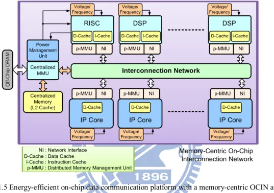
RISC Centralized Memory (L2 Cache) D-Cache I-Cache Centralized
MMU Interconnection Network
Voltage/ Frequency DSP D-Cache I-Cache Voltage/ Frequency D-Cache IP Core Power Management Unit DSP D-Cache I-Cache Voltage/ Frequency IP Core IP Core Memory-Centric On-Chip Interconnection Network Voltage/
Frequency FrequencyVoltage/ FrequencyVoltage/
p-MMU : Distributed Memory Management Unit NI : Network Interface
D-Cache : Data Cache I-Cache : Instruction Cache
D-Cache D-Cache p-MMU NI p-MMU NI p-MMU NI p-MMU NI p-MMU NI p-MMU NI
Fig. 1.5 Energy-efficient on-chip data communication platform with a memory-centric OCIN and an on-demand memory sub-system.
Based on the above crucial issues in multi-core SoCs, including the energy bound and the increasing requirements of data communication and data storage, an energy-efficient on-chip data communication platform is proposed in this dissertation as shown in Fig. 1.5. This on-chip data communication platform consists of a memory-centric OCIN and an on-demand memory sub-system. The memory-centric OCIN provides building blocks with on-demand memory sub-systems, including energy-efficient and reliable channels, congestion-aware routing algorithm, energy-efficient routing table, two-level FIFO buffer and buffer-efficient NIs. In addition, the on-demand memory sub-system provides high bandwidth and low power memory accesses for multi-core SoCs via a centralized memory management unit
(c-MMU) and private memory management units (p-MMUs). The on-demand memory sub-system can support variety memory resources for different PEs based on the memory behaviors. Moreover, when decoding the video frames, memory access characteristics of video decoders are generally regular and repeat. Therefore, the on-demand memory sub-system can improve the decoding performance via efficient memory management. Memory-Centric On-Chip Data Communication Memory-Centric On-Chip Interconnection Network Routers Network Interfaces
Two-Level FIFO Buffer (Chap 4) 1. Synchronous two-level FIFO buffer 2. Asynchronous two-level FIFO buffer Congestion-Aware Routing (Chap 5) 1. Adaptive routing for mesh-network Implementation of Routing Table (Chap 6) 1. Routing table in OCINs
2. Extended Routing Table in IPv6 Applications Energy-Efficient Reliable Channels (Chap 3) 1. Self-corrected green coding
2. Self-calibrated voltage scaling
Efficient Network Interface (Chap 7) 1. Borrowing mechanism for network interface
Link Wires
On-Demand Memory Sub-System
Distributed Memory Management Unit (Chap 7) 1. Borrowing mechanism network interface 2. Inter-layer pre-fetch for scalable video coding
Centralized Memory Management Unit (Chap 7) 1. Adaptive cache control
2. Efficient external memory interface for DDR3 3. Efficient address translator
p-MMUs c-MMU Data Storage Multi Processor Elements Data Computation Multi-Core SoC Data Communication
Network Interface provides a bridge between data computation, data storage and data communication.
Energy-Efficient Multi-Core SoC Designs
Fig. 1.6 The contribution matrix of energy-efficient memory-centric on-chip data communication
1.2 Contributions of This Dissertation
In this dissertation, an energy-efficient memory-centric on-chip data communication platform is proposed to deal with the increasing data communication and data storage for heterogeneous multi-core SoC designs. Fig. 1.6 presents the contribution matrix of energy-efficient memory-centric on-chip data communication which consists of a memory-centric OCIN and an on-demand memory sub-system. The memory-centric OCIN provides the micro-architecture for data communication
based on the building blocks, including link wires, routers and NIs. In this dissertation, all building blocks are analyzed and developed to realize energy-efficient multi-core SoCs. Additionally, the on-demand memory sub-system enhances memory bandwidth and reduces the total execution time of the whole system via the centralized MMU and private MMUs. Moreover, the NI provides a bridge between the on-demand memory sub-system, memory-centric OCIN and heterogeneous PEs. The contributions of each block are described as follows.
1.2.1 Link Wires
For link wires, a novel self-calibrated energy-efficient and reliable channel design is proposed for OCINs. The proposed channels reduce the energy consumption while maintaining reliability. The channels are developed using the self-calibrated voltage scaling technique with the self-corrected green (SCG) coding scheme. The SCG coding is a joint bus and error correction coding scheme that provides a reliable mechanism for channels. In addition, it achieves a significant reduction in energy consumption via a joint triplication bus power model for crosstalk avoidance. Based on SCG coding scheme, the proposed self-calibrated voltage scaling technique adjusts voltage swing for energy reduction. Furthermore, this technique tolerates timing variations.
1.2.2 Routers
Routers are the essential components of OCINs. The router architecture depends on the topology and flow control of OCINs. A generic router architecture consists of a set of input buffers, an interconnect matrix, a set of output buffers and control circuitries, including a routing controller, an arbiter and an error detector. In this thesis, a data-link two-level FIFO (first-in first-out) buffer architecture with the centralized
shared buffer is proposed in this paper. The proposed two-level FIFO buffer architecture has a shared buffer mechanism allowing the output channels to share the centralized FIFO with sufficient buffer space. Additionally, the proposed architecture reduces the area and power consumption to achieve the same performance.
In addition to the proposed two-level FIFO buffer, an adaptive congestion-aware routing algorithm with a quality-of-service guarantee arbitration mechanism is proposed for mesh OCINs. Depending on the traffic around the routed node, the proposed routing algorithm provides not only minimum paths but also non-minimum paths for routing packets. Both minimum and non-minimum paths are based on the odd-even turn model to avoid deadlock and livelock problems. The decision of the minimum paths or non-minimum paths depends on the utilities of buffers in neighbor nodes and the specific switching value. In this adaptive algorithm, the congestion conditions and distributed hotspots will be avoided. It has the advantages of getting higher performance and also reducing the latency.
The implementation of routing tables is also proposed via content addressable memories (CAM). Moreover, the implementation of routing tables is extended for IPv6 network routers, which is the next generation of network routers, using ternary content addressable memories (TCAM). As routing tables become larger, energy consumption and leakage current become increasingly important issues in the design of TCAM in nano-scale technologies. Therefore, a novel energy-efficient TCAM macro design is proposed for IPv6 applications. The proposed TCAM employs the concept of architecture and circuit co-design. To achieve an energy-efficient TCAM architecture, a butterfly match-line scheme and a hierarchy search-line scheme are developed to reduce significantly both the search time and power consumption. The match-lines are also implemented using noise-tolerant XOR-based conditional
keepers to reduce not only the search time but also the power consumption. To reduce the increasing leakage power in advanced technologies, the proposed TCAM design utilizes two power gating techniques, namely super cut-off power gating and multi-mode data-retention power gating.
1.2.3 Network Interfaces
NIs, one of the building blocks in OCINs, is a major factor in the performance. In this dissertation, an efficient NI is proposed for the memory-centric OCIN to reduce the data blocking by a borrowing mechanism. By considering the borrowed memory blocks and p-MMU, the size of the output queue in NI can be dynamically scheduled. Additionally, the p-MMU can dynamically allocate the memory resources for buffering the blocking network data. Therefore, the proposed efficient NI can increase the performance of the memory-centric OCIN.
1.2.4 On-Demand Memory Sub-system
In this dissertation, a memory-centric on-chip data communication platform is presented for merging heterogeneous PEs, and applied to wireless video entertainment systems. In this platform, on-demand memory sub-system is developed for dynamically allocating memory resources and efficiently managing memory accesses. The contributions of on-demand memory sub-system are described as follows.
A. Buffer borrowing mechanism for NIs
In order to reduce the stall of PEs caused by network data blocking, a novel buffer borrowing mechanism is proposed to borrow the memory resources for buffering the blocking packets.
For multi-task applications, different processor elements (PEs) may have different memory requirements during runtime. Therefore, the proposed c-MMU can support memory resource re-allocation by adaptive cache control scheme. Accordingly, the memory utilization of the system can be improved.
C. External Memory Interface for DDR3 DRAM
DDR3 DRAM devices are utilized for supporting huge data storage recently. Therefore, an efficient external memory interface (EMI) is also designed to reschedule read/write commands for DDR3 DRAM that reduces both execution time and energy consumption.
D. Inter-Layer Pre-Fetch Scheme for Scalable Video Coding
For wireless video entertainment systems, a scalable video coding (SVC) is utilized to adapt variations of wireless channels. Based on the data stream of SVC, an inter-layer pre-fetch scheme (IPS) is proposed to reduce the miss rate during frame decoding of SVC.
E. Efficient Address Translator (AT) for SVC
The SVC data allocation in DDR3 DRAM is proposed using an efficient address translator. The translated addresses can improve the DRAM access efficiency while processing SVC.
1.3 Organization of This Dissertation
The organization of this dissertation is depicted as follows. The related works of on-chip data communication are introduced in Chapter 2. In this chapter, the concept of on-chip data communication and previous works of the NoC/ OCIN are described. After presenting the related works of on-chip data communication, Chapter 3 presents
the self-calibrated energy-efficient and reliable channel design for OCINs using a self-calibrated voltage scaling technique with a SCG coding scheme. In the beginning of this chapter, previous reliable and low power coding schemes are analyzed. Then, the self-calibrated low power coding and voltage scaling channels are presented in the following sections.
Chapter 4 presents the synchronous and asynchronous two-level FIFO buffers in routers for OCINs. The proposed two-level FIFO buffer architecture has a shared buffer mechanism allowing the output channels to share the centralized FIFO with sufficient buffer space. Different buffer architectures and different circuit implementations are analyzed and compared in the beginning of this chapter. Then, the concept of the proposed two-level FIFO buffer architecture is presented. The next section describes the behavior and circuit implementation of the data-link two-level FIFO buffer for the router. Consequently, the asynchronous and associated two-level FIFO buffer architectures are described in the following sections.
An adaptive congestion-aware routing algorithm is described in Chapter 5. In the first section of this chapter, the related works of routing algorithms are introduced and compared. The concept of the proposed routing algorithm for a router is presented in the following section. Then, the detail of the proposed adaptive congestion-aware routing algorithm and its implementation are both described. In addition, the quality-of-service arbitration mechanism is also be presented in next section.
And then, the implementation of routing tables in OCINs is presented in the first section of Chapter 6. Moreover, the implementation of routing tables is extended for network routers in IPv6 applications via a TCAM macro. In this chapter, the overall architecture of the TCAM macro design is introduced. Then, the following section introduces the proposed energy-efficient match-line schemes, which involve the
butterfly match-line and XOR-based conditional keeper. Next, the proposed don’t-care-based hierarchy search-line scheme will be presented. Furthermore, the next section elucidates two power gating techniques for reducing leakage current.
Subsequently, Chapter 7 presents the design of the on-demand memory sub-system, including p-MMUs and a c-MMU. Buffer borrowing mechanism in p-MMUs and adaptive cache scheme in the c-MMU are proposed for optimizing the memory resources utilization dynamically. Additionally, for accessing the external memory, an efficient external memory interface is presented. Subsequently, a pre-fetch and DRAM data allocation schemes are described to improve the memory energy efficiency in wireless video entertainment systems. Therefore, a pre-fetch command generator and an address translator are applied in p-MMUs and c-MMU, respectively. Finally, conclusions are finally drawn in Chapter 8, along with recommendations for future research.
Chapter 2:
Survey of On-Chip Data Communication
With development of System-on-Chip (SoC) and multimedia communication technologies, a great amount of data computing requirement increases rapidly. In addition, the communication bandwidth requirement between processor elements (PEs) and the memory bandwidth requirement are also increasing to maintain the system performance. Therefore, the aggregate communication bandwidth between the processing cores is in the GBytes/s range for many video applications. In the future, with the integration of many applications onto a single device and with increased processing speed of cores, the bandwidth demands will scale up to much larger values. Multi-core SoC architectures are emerging as appealing solutions for embedded multimedia applications [2.1]-[2.5]. In general, multi-core SoCs are composed of core processors, memories and some application-specific cores. Additionally, data communication among PEs is provided by advanced interconnect fabrics, such as high performance and efficient networks-on-chip (NoCs) [2.6]. NoC was investigated for dealing with the challenges of on-chip data communication caused by the increasing scale of next generation SoC designs. Furthermore, on-chip interconnection networks (OCINs) provide the micro-architecture and the building blocks for NoCs, including network interfaces (NIs), routers and link wires [2.7], [2.8]. In OCINs, PEs (including memory modules) communicate by sending packet to one another over the network instead of by sending wires over ad-hoc wiring structures [2.9]. In this chapter, the related works of on-chip data communication are given, including NoCs, OCINs and memory sub-systems. The organization of this chapter is as shown in Fig. 2.1.
Fig. 2.1 The organization of Chapter 2.
2.1 Why NoC and OCIN?
Multi-core SoC designs provide the integrated solution in the communications, multimedia and consumer electronics. Moreover, SoC designs become increasingly complex, while the associated numbers of transistors grows exponentially. Most SoC will find their application within embedded systems, traditional figures of merit, such as performance, energy consumption and cost. However, modern SoC design is faced with a number of problems caused by the scale and complexity of the designs although on-chip bus platforms provide interfaces between PEs and a good verification environment as shown in Fig. 2.2.
Fig. 2.2 A conventional on-chip bus platform. [2.10]
First, the complexity of on-chip bus platforms increases exponentially while the number of PEs increases linearly [2.10]. The shared bus architectures limit the
development factor for integration with increasing PEs. Existing bus architectures and techniques are proving to be non-scalable, unable to meet leading edge complexity and performance requirements. Second, the interconnect delay across the chip exceeds the average clock period of the IP blocks, especially in nano-scale technologies [2.11]. The ratio of global interconnect delay to average clock period will continue to grow. An interconnect channel design methodology for high performance ICs has proposed in [2.11], it devised a methodology to size the FIFOs in an interconnect channel containing one or more FIFOs connected in series and shows that the sizing of the FIFOs in the channel is a function of system parameters such as data production rate and communication rate, number of channel stages etc.
Third, in nano-scale technologies, increased coupling effect for interconnects not only aggravates the power-delay metrics but also deteriorates the signal integrity due to capacitive and inductive crosstalk noises [2.11].Several options were proposed to reduce the inter-wire capacitances. The first option is to widen the pitch between bus lines. The second option is using P&R (place & route) tools to avoid routing of the bus lines side by side. However, the interconnect complexity and the routing time do not allow designers trying it to minimize the coupling capacitances. The third option is to change the geometrical shape of bus lines. But the disadvantage of this method is that the frank area will increase since the cross-sectional area of a bus line is fixed. The fourth technique is to add a shielding line (VDD/Ground) between two adjacent signal lines. The fifth option reduces the coupling power consumption via bus encoding schemes [2.12]-[2.16]. However, on-chip physical interconnections will present a limited factor for performance, reliability and energy consumption due to advanced technologies [2.17], [2.18]. Therefore, the encoding schemes for low power and reliability issues were proposed in [2.19], [2.20]. The designers must overcome
the challenge of noises to provide the function correct, reliable operation of the interacting components. A robust self-calibrating transmission scheme for interconnections is proposed in [2.21] and it examines some physical properties of on-chip interconnects, with the goal of achieving fast, reliable and low-energy communication.
Forth, both the system design and performance are limited by the complexity of the interconnection between the different modules and blocks into single clocked design. Different data transfer speeds are required, as well as parallel transmission. The traditional system buses may not be suitable for such a system since only one module can transmit at a time. Additionally, modern multi-core SoC designers assemble the system using ready virtual components which might not be easily adaptable to different clocking situations. The solution to above problems is a segmented bus design combined with the concept of the globally asynchronous locally synchronous (GALS) system architecture [2.22]-[2.24]. Asynchronous design can make the circuits resilient to delay variation.
Fig. 2.3 Multi-layer bus architecture. [2.24]
For the above mentioned problems, new architectures for on-chip data communications were proposed to adapt the next multi-core SoC era. A multi-layer on-chip shared bus, as shown in Fig. 2.3, was proposed as an advised version of the
Master #1 Master #2 Master #3 Bus Matrix Slave #1 Slave #2 Slave #3
conventional on-chip bus platform to reduce the shared-medium channels [2.24]-[2.26]. Multi-layer on-chip buses enable parallel access paths between multiple masters and slaves by a bus matrix. However, multi-layer bus architectures are confused with complex wire routings inducing larger power consumption and interconnect delay associated with the increasing number of PEs.
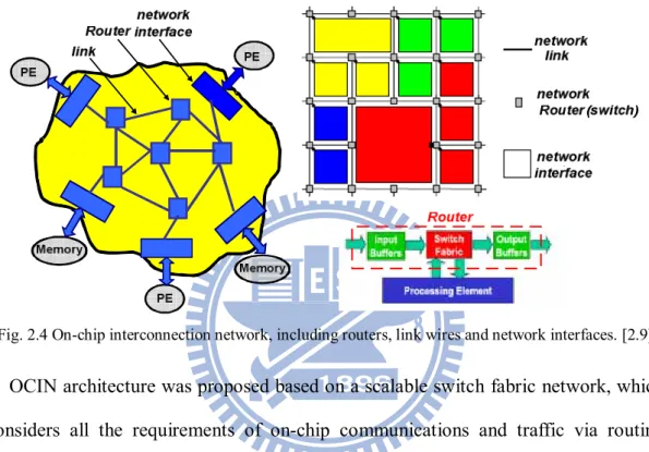
Fig. 2.4 On-chip interconnection network, including routers, link wires and network interfaces. [2.9]
OCIN architecture was proposed based on a scalable switch fabric network, which considers all the requirements of on-chip communications and traffic via routing packets [2.9]. Moreover, OCINs have a few distinctive characteristics, namely low communication latency, energy consumption constraints and design-time specialization. Fig. 2.4 presents the OCIN architecture that provides the building blocks and backbone for NoC platform. The motivation of establishing NoC platform is to achieve performance using a system perspective of communication. The core of NoC technology is the active switching fabric that manages multi-purpose data packets within complex, IP laden designs.
2.2 Design Abstraction Levels of NoC
communication and the abstraction of NoC as a micro-network and analyzing the various levels of this micro-network stack bottom to up is as shown in. NoC models are typical organized starting from physical layer to software layer, in a fashion that resembles the Open Systems Interconnection (OSI) model as shown in Fig. 2.5 [2.27]-[2.28]. However, the OSI model stacks is resembled for a marco-network. For a micro-network, the model stack will be reduced to four layers, namely physical layer, data-link layer, network and transport layer (transaction layer) and software layer [2.29]. Fig. 2.6 shows the reduced NoC protocol stack, and the physical layer, data-link layer, and transaction layer present the design models for OCIN, which constructs the micro-architecture for NoC. Moreover, the research of OCIN can further be divided into micro-architectural innovations within the major components
Fig. 2.5 The design abstraction layers of NoC [2.27]
and macro-architectural choices aiming to seamlessly merge the interconnection backbone with the remaining system modules [2.30].
NoC protocols are described bottom-up, starting from the physical layer up to the application layer. In the physical layer, link wires are the physical implementation of the communication channels. It is important to realize that a well-balanced design should not over design wires so that their behavior approaches an ideal one, because that the corresponding cost in performance, energy-efficiency and modularity may be too high. Physical layer design should find a compromise between competing quality metrics and provide a clean and complete abstraction of channel characteristics to layers above.
NoC design entails the specification of network architectures and control protocols. The data-link layer abstracts the physical layer as an unreliable digital link, where the probability of bit upsets is non null. Furthermore, reliability can be traded off for energy. The main purpose of data-link protocols is to increase the reliability of the link up to a minimum required level, under the assumption that the physical layer by itself is not sufficiently reliable. At the data link layer, error correction can be complemented by several packet-based error detection and recovery protocols. Several parameters in the protocols can be adjusted depending on the goal to achieve maximum performance at a specified residual error probability within given energy consumption bounds.
At the network and transport (transaction) layer, packet data transmission can be customized by the choice of switching and routing algorithms. The NoC designers establish the type of connection to its final destination. Switching and routing affect heavily performance and energy consumption. Robustness and fault tolerance will also be highly desirable. Algorithms deal with the decomposition of messages into
packets at the source and their assembly at destination. Packetization granularity is a critical design decision because the behavior of most network control algorithm is very sensitive to packet size. Packet size can be application specific in SoCs, as opposed to general network.
Software (application) layers comprise system and application software which includes PEs and network operating systems. The system software provides us with an abstraction of the underlying hardware platform. Moreover, policies implemented at the system software layer request either specific protocols or parameters at the lower layers to achieve the appropriate information flow. The hardware abstraction is coupled to the design of wrappers for processor cores which perform as network interfaces between PEs and NoC architecture.
Fig. 2.7 Data abstraction. [2.7]
Fig. 2.8 NoC research areas versus OSI model based on the flow of data. [2.31]
2.7, which are message, packet, flit and phit (physical transfer unit) [2.7]. Therefore, in addition to the reduced design abstraction layers, the spectrum of NoC research is also divided into four areas based on the flow of data, including system, network adapter, network and link [2.31]. The correspondence between these four areas and OSI models is as shown in Fig. 2.8. The network adapter provides a bridge between high-level services and communication primitives using core interfaces (CIs) and NIs.
Fig. 2.9 NoC Research category based on design abstraction layers and flow of data abstraction. [2.31]
According to the design abstraction layers and flow of data, the NoC research topics can be categorized as shown in Fig. 2.9 [2.31], [2.32]. In the following sections, the research topics associated with OCINs are introduced, including both macro-architectural exploration (topology) and micro-architectural exploration (building blocks). Moreover, the research related to power analysis, voltage scaling and GALS of NoC is also described.
2.3 Network Topologies of OCINs
NoC platforms enable designing parallel systems resembling cellular structures including thousands of PEs. Such systems combined with multi-threaded computing can increase system efficiency for fine-grain parallel programs [2.33], [2.34]. Therefore, the OCIN architecture of NoC should be efficient for a huge amount of
PEs. A number of different OCINs have been proposed as shown in Fig. 2.10. Their origins can be traced back to the field of parallel computing. However, a different set of constraints exists when adapting these architectures to the muli-core SoC design paradigm. (c) (b) (a) (f) (e) (d)
Fig. 2.10 Conventional network topologies of OCIN (a) SPIN (b) Mesh (c) Torus (d) Folded tours (e) Octagon (f) Butterfly Fat tree. [2.35]
A generic interconnect template was proposed which is called SPIN (Scalable, Programmable, Integrated Network) for on-chip packet switched interconnections as shown in Fig. 2.10(a), where a fat-tree architecture is used to interconnect PEs [2.35]. In this fat tree, every node has four children and the parent is replicated four times at any level of the tree. The functional PEs reside at the leaves and the switches reside at the vertices. A mesh-based (tile-based) OCIN architecture consists of an m x n mesh of switches interconnecting computational resources (PEs) placed along with the switches, as shown in Fig. 2.10(b). Every switch (router), except those at the edges, is connected to four neighboring switches and one PE.
architecture is basically the same as a regular mesh. The only difference is that the switches at the edges are connected to the switches at the opposite edge through wrap-around channels. Every switch has five ports, one connected to the local resource and the others connected to the closest neighboring switches. The long end-around connections can yield excessive delays. However, this can be avoided by folding the torus as Fig. 2.10(d) [2.37]. This renders to a more suitable VLSI. The OCTAGON MP-SoC architecture was proposed in [2.38]. Fig. 2.10(e) shows a basic octagon unit consisting of eight nodes and 12 bidirectional links. Each node is associated with a processing element and a switch. Communication between any pair of nodes takes at most two hops within the basic octagonal unit. For a system consisting of more than eight nodes, the octagon is extended to multidimensional space. This type of interconnection mechanism may significantly increase the wiring complexity. In a Butterfly Fat-Tree (BFT) architecture which is shown as Fig. 2.10(f), PEs are placed at the leaves and switches placed at the vertices [2.39]. A pair of coordinates is used to label each node. The number of switches in the butterfly fat tree architecture converges to a constant independent of the number of levels. Other high-radix topologies were also studied as OCIN architectures [2.40], [2.41]. However, the complexity of the switching circuits in high-radix topologies induces huge amount of area and power consumption.
A popular network topology of OCIN implementations is the two-dimensional mesh architecture as mentioned above, providing a regular topology and communications. Therefore, many advanced OCIN topologies are designed based on this mesh network. An advanced OCIN, called Xpipes as shown in Fig. 2. 11, targeting high performance and reliable communication for on-chip multi-processors was presented in [2.42]. Data links can be pipelined with a flexible number of stages to decouple link throughput from its length and to get arbitrary topologies. The I/O ports of each switch can be parameterized, and Xpipes is optimized from mesh-based OCIN architecture.
Fig. 2.12 A Hierarchical OCIN architecture. [2.43]
A hierarchical OCIN architecture was presented and constructed via local network and global network as shown in Fig. 2.12 [2.43]. The local network preserves the features of 2-D links network on chip, and the global network is designed as centralized crossbar. Other hierarchical OCIN or hybrid OCIN topologies were also proposed to adopt multiple PEs and heterogeneous systems [2.44]-[2.47]. Energy consumption and area of hierarchical OCIN architectures were analyzed as shown in Fig. 2.13 [2.48]. Fig. 2.13(a) shows the comparison result of the energy consumption under the uniform traffic. Although the mesh has short and regular length of links, it has more hop counts than the star thus the energy cost of the mesh is 40%-50% higher
![Fig. 2.20 A bi-direction channels to optimize the utilization of link wires. [2.74]](https://thumb-ap.123doks.com/thumbv2/9libinfo/8466174.183357/59.892.162.733.524.960/fig-bi-direction-channels-optimize-utilization-link-wires.webp)
![Fig. 2.29 Block diagram of network interface supporting the CTC protocol. [2.121]](https://thumb-ap.123doks.com/thumbv2/9libinfo/8466174.183357/69.892.234.663.529.797/fig-block-diagram-network-interface-supporting-ctc-protocol.webp)
![Fig. 2.33 A methodology for managing power consumption of NOCs via the estimator. [2.136]](https://thumb-ap.123doks.com/thumbv2/9libinfo/8466174.183357/73.892.136.756.474.893/fig-methodology-managing-power-consumption-nocs-estimator.webp)