國 立 交 通 大 學
光電工程學系碩士班
碩士論文
有機無機電晶體應用於氣體感測之研究
Organic and Inorganic Transistors for Gas Sensing
研究生:余治寬
指導教授:冉曉雯 教授
蔡娟娟 教授
有機無機電晶體應用於氣體感測之研究
Organic and Inorganic Transistors for Gas Sensing
研 究 生:余治寬 Student:Chih-Kuan Yu
指導教授:冉曉雯 教授 Advisor:Prof. Hsiao-Wen Zan
蔡娟娟 教授 Prof. Chuang-Chuang Tsai
國 立 交 通 大 學
光電工程學系碩士班
碩 士 論 文
A Thesis
Submitted to Institute of Electro-Optical Engineering
College of Electrical Engineering and Computer Science
National Chiao Tung University
in Partial Fulfillment of the Requirements
for the Degree of Master
in
Electro-Optical Engineering
July 2012
Hsinchu, Taiwan, Republic of China
i
有機無機電晶體應用於氣體感測之研究
研究生:余治寬 指導教授: 冉曉雯 教授 蔡娟娟 教授 國立交通大學光電工程學系碩士班摘要
在本研究中,我們首先將介紹一個有機垂直通道空間電荷限制電晶體的氣體感測器。 透過具備氧化或還原特性的氣體對電晶體的主動層造成電子摻雜或電子解摻雜的效應, 進而改變垂直通道中的電位分佈,導致輸出電流密度的改變。藉由對於氨氣具備 30 ppb 的感測極限,此氣體感測器將可以應用在被非侵入式呼氣監控的定點照護檢驗。 此外,一個無機非晶銦鎵鋅氧化物薄膜電晶體混合式氣體感測器也將被介紹。我們 將金屬氧化物半導體覆蓋在電晶體的背通道上面,作為氣體感測層以及第二個閘極。透 過接觸具備氧化或還原特性的氣體分子,電荷將會在感測層和氣體分子間傳遞,造成感 測層的位能改變,使得第二個閘極的電位改變,導致輸出電流改變。此無機混合式氣體 感測器對於氨氣和一氧化氮的感測極限分別為 50 ppb 和 3ppm。 最後,我們將在附錄中介紹提升非晶銦鎵鋅氧化物薄膜電晶體載子遷移率的初步結 果。透過使用飛秒雷射照射非晶銦鎵鋅氧化物薄膜表面,我們可以得到一個高載子遷移 率(~84 cm2 /Vs)的電晶體。其可能原因為,飛秒雷射照射非晶銦鎵鋅氧化物薄膜後,會 造成通道導電率的提升,進而使得載子遷移率提升。ii
Organic and Inorganic Transistors for Gas Sensing
Student : Chih-Kuan Yu Advisor: Prof. Hsiao-Wen Zan Prof. Chuang-Chuang Tsai
Department of Electro-Optical Engineering National Chiao Tung University
Abstract
In this thesis, we report a very sensitive gas sensor embedded in a vertical polymer
space-charge-limited transistor at first. The oxidizing and reducing gases act as electron dedoping and electron doping agents on the transistor active layer to change the potential
distribution in the vertical channel and hence to change the output current density. With a 30-ppb detection limit to ammonia, the sensor can be used for non-invasive breath monitor in
point-of-care applications.
In addition, a metal-oxide sensing layer is capped onto an amorphous indium gallium
zinc oxide (a-IGZO) thin-film transistor (TFT) to form a hybrid sensor. The metal-oxide layer, served as a second gate, forms a p-n junction with a-IGZO film. Oxidizing or reducing vapor
molecules act like electron acceptors or electron donors to change the potential of the metal-oxide layer and the current of a-IGZO TFT. A sensitive response to 50 ppb ammonia
and 3 ppm nitric oxide is obtained.
In the end, a preliminary result of femtosecond laser irradiation (FLI) on a-IGZO TFTs is
demonstrated in appendix. A high mobility (~84 cm2/Vs) top-gate (TG) a-IGZO TFT is
proposed. It is supposed that FLI on a-IGZO film induces an increase in channel conductivity
iii
誌謝
時光匆匆,碩班生活就這樣結束了。不同於一般的碩士生,我選擇了五年學碩這一 條路,這是一條生活非常充的路。在別人眼裡悠哉的大四這年,身兼大四生和碩一生的 我,背負著二十四個碩班學分和修學完的專選學分。為了能夠再碩二能全心做實驗,雨 大二生沒有兩樣。回首過去的二十三年,非常感謝我的爸媽無私的照顧。還記得在那腸 胃炎,發燒,及打球扭傷的時刻,老爸老媽總是及時的伸出援手。此外,在經濟上全力 的支持,讓我不用為了吃和生活去打工,可以全心投入學業。對於老爸和老媽,我有說 不完的感謝和感激。 打從專題研究開始,冉老師的細心指導以及不離不棄,讓我感到格外的溫暖和感激。 在這和冉老師相處的兩年半時光裡,很慶幸沒有讓老師為了我而大動肝火。非常感謝老 師在研究上的指導和建議,沒有這兩年的磨練,或許就不會有今天比較有耐心,比較細 心,和比較有點專業知識的我。此外我也要感謝孟老師和洪老師的適時指導。 感謝每一位學長姐,同學和學弟妹真誠的對待。在我們實驗室裡,我沒有感受到別 人傳言中的研究所的冷淡和自私,相反的卻是慢慢的人情味。或許大家的實驗都很忙碌, 但是在需要幫忙時總是可以找到幫助。首先我想感謝銘志學長從專題生到現在不時的建 議和幫助,讓我在最無助的時候找到方向。感謝長紘一起度過大半的碩二生活,如果沒 有你的陪伴、幫忙和建議,我的碩班生涯應該會是悲慘世界。感謝所有幫我量過膜厚的 大家:浩文、宇帆、郁茜、俊閔、永軒、和郁馨。感謝良豪和峻宏,換檔板、清腔和蝕 刻如果沒有你們的互相照應,這些日子應該會是很難熬。感謝電晶體、Sensor、LED、 IGZO、Solar 組以的各位以及助理們。最後,要特別感謝洪銓!謝謝你在我碩二的後半 段回歸做 IGZO 時,陪伴幫忙量測以及接下採購量測機台的工作,辛苦你了加油!碩班的這些日子裡,做過 Sensor,SCLT solar cell,SCLT sensor,和 IGZO TFT , 可以說除了 LED 以外,其他各組的東西都摸索過一點皮毛。真的很感謝有機實驗室的
iv
Contents
摘要 ... i Abstract ... ii 誌謝 ... iii Contents ... ivFigures Captions ... viii
Table Captions ... xiii
Chapter1 - Introduction ... 1
1.1 Organic Semiconductor Materials ... 1
1.1.1 Hole Transport Material – Poly(3-hexylthiophene) ... 2
1.1.2 Insulator Layer – Poly(4-vinyphenol) ... 3
1.2 Vertical Organic Semiconductors... 3
1.3 Application of Metal Oxide Semiconductor for Sensing ... 4
1.4 Metal Oxide Semiconductor Thin Film Transistors ... 5
1.5 Motivation ... 6
1.5.1 Space Charge Limited Transistor (SCLT) Sensor ... 6
1.5.2 Amorphous IGZO TFT Hybrid Sensor ... 7
Figures of Chapter 1 ... 8
Chapter2 - Theoretical Background ... 10
2.1 Metal-Semiconductor Junction ... 10
2.2 Charge Transportation of Organic Conjugated Polymer ... 11
2.2.1 Bulk Limited and Space Charge Limited Current Theories ... 12
2.2.2 Thermionic Emission Theory and Tunneling Effect ... 13
v
2.4 Carrier Transport Mechanism of Metal-Oxide Semiconductors ... 16
2.5 Methods of Device Parameters Extraction ... 18
2.5.1 Mobility (μ) ... 18
2.5.2 Turn-On Voltage (Von) ... 19
2.5.3 Threshold Voltage (VTH) ... 19
2.5.4 Ion/Ioff Current Ratio ... 20
2.5.5 Sub-Threshold Swing (S.S.) ... 20
Figures of Chapter 2 ... 21
Chapter3 - Device Structure, Fabrication, and Experiment Setup ... 25
3.1 Introduction ... 25
3.2 Methods of Device Parameters Extraction ... 25
3.2.1 Glass Substrate Cleaning ... 25
3.2.2 ITO Patterning ... 26
3.2.3 ITO Surface Planarization ... 27
3.2.4 Insulator Layer ... 27
3.2.5 Sacrificing Layer ... 27
3.2.6 Spin-Rinse ... 28
3.2.7 Adherence of Polystyrene ... 28
3.2.8 Porous Base Electrode ... 28
3.2.9 Vertical Channel ... 28
vi
3.2.11 Porous Collector Electrode ... 29
3.3 Amorphous IGZO TFT Hybrid Sensor ... 29
3.3.1 Gate Dielectric Layer ... 30
3.3.2 Substrate Cleaning ... 30
3.3.3 a-IGZO Film Deposition... 31
3.3.4 Post-Annealing ... 31
3.3.5 Source/Drain Deposition ... 31
3.3.6 Sensing Layer Capping ... 32
3.4 Micro-Fluid Gas Sensing Measurement System ... 32
3.5 Analysis Instruments ... 33
3.5.1 Current-Voltage Measurement Instruments ... 33
3.5.2 Radio Frequency Magnetron Sputter ... 33
Figures of Chapter 3 ... 34
Chapter4 - Results and Discussion ... 37
4.1 Space Charge Limited Transistor (SCLT) Sensor ... 37
4.1.1 Characteristics of Porous SCLT ... 37
4.1.2 Ammonia Sensing Results ... 38
4.1.3 Nitric Oxide Sensing Results ... 42
4.1.4 TCAD SILVACO ATLAS Simulation ... 43
4.2 Amorphous IGZO TFT Hybrid Sensor ... 46
4.2.1 Ammonia Sensing Results ... 47
vii
Figures of Chapter 4 ... 49
Chapter5 - Conclusion and Future work ... 63
5.1 Conclusion ... 63
5.2 Future Work ... 64
Appendix ... 65
A.1 Effective Mobility Enhancement Induced by Femtosecond Laser Irradiation in a-IGZO TFT ... 65
A.1.1 Abstract ... 65
A.1.2 Motivation ... 65
A.1.3 Device Fabrication ... 66
A.1.4 Results and Discussion ... 67
A.1.5 Conclusion and Future Work ... 67
Figures of Appendix ... 69
viii
Figures Captions
Fig. 1-1 Chemical structure polyacetylene (PA). ... 8
Fig. 1-2 Chemical structures of (a) P3HT monomer (b) P3HT polymer. ... 8
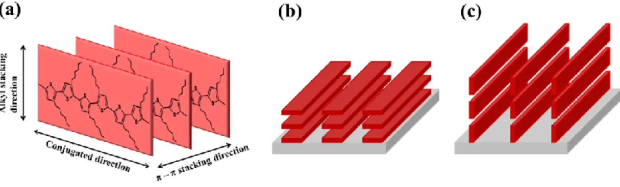
Fig. 1-3 (a) The Schematic diagram of P3HT conjugation direction, π-π stacking direction and alkyl stacking direction (b) Plane-on stacking of P3HT. (c) Edge-on stacking of P3HT. ... 8
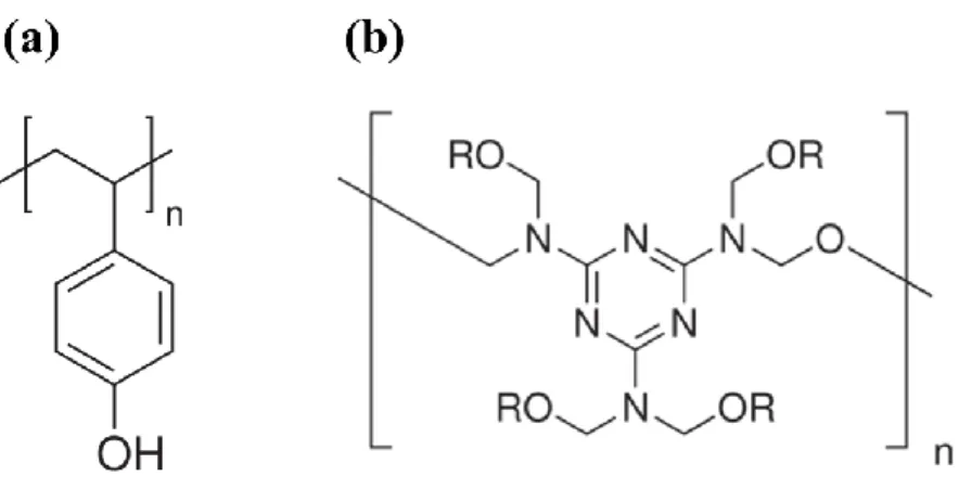
Fig. 1-4 Chemical structures of PVP and PMF. (a) PVP and (b) PMF. ... 9
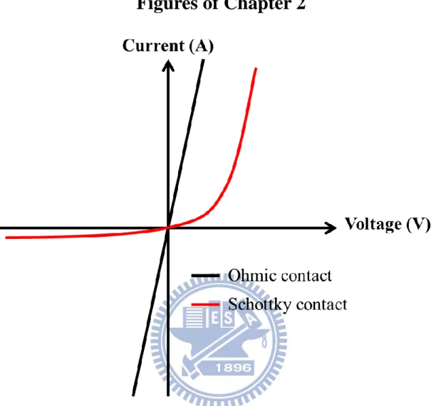
Fig. 2-1 The characteristics of current as a function of voltage. Both ohmic contact and schottky contact are shown. ... 21
Fig. 2-2 Band diagram of schottky contact... 21
Fig. 2-3 Band diagram of ohmic contact... 22
Fig. 2-4 Schematic diagram of thermionic emission theory. ... 22
Fig. 2-5 Schematic diagram of tunneling effect. ... 22
Fig. 2-6 Development of space charge limited transistor (SCLT) from field effect transistor. ... 23
Fig. 2-7 Structures of bottom-injection and top-injection SCLTs. (a) Bottom-injection SCLT, emitter is ITO and Al is collector. (b) Top-injection SCLT, emitter is MoO3/Al and collector is ITO. ... 23
ix
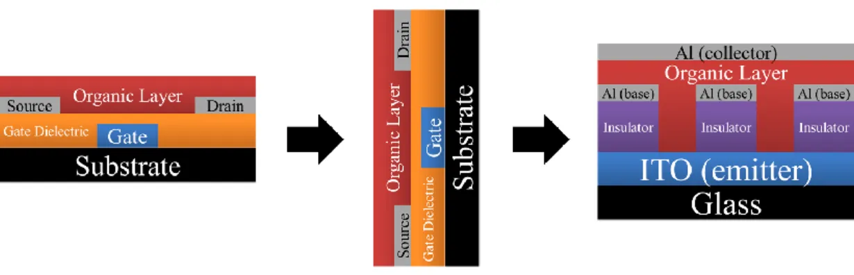
Fig. 2-8 The relationship between operation of SCLT and band diagrams. (a) On state of
SCLT. (b) Off state of SCLT. ... 24
Fig. 2-9 (a) The relationship between log(Ne) and activation energy (Ea). The straight line is the result fitted to the exponential tail density of state model. (b) Schematic energy diagram near the conduction band edge and the density of state for sc-IGZO [34]. ... 24
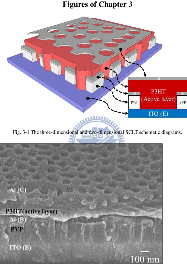
Fig. 3-1 The three-dimensional and two-dimensional SCLT schematic diagrams. ... 34
Fig. 3-2 The SEM cross-section image of SCLT. ... 34
Fig. 3-3 The flowchart of the fabrication processes of SCLT sensor. ... 35
Fig. 3-4 Two-dimensional a-IGZO TFT hybrid sensor schematic diagram. ... 35
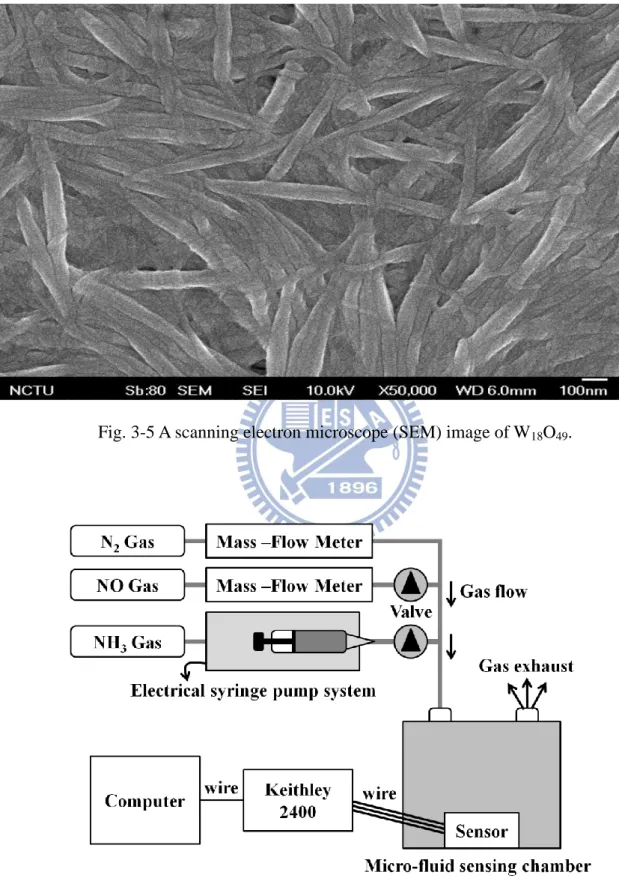
Fig. 3-5 A scanning electron microscope (SEM) image of W18O49 ... 36
Fig. 3-6 Micro-fluid gas sensing measurement system. ... 36
Fig. 4-1 The diode characteristics of porous SCLT, including EC, EB and BC diode. (a) EC diode characteristics between emitter and collector where emitter is biased and collector is grounded. (b) EB diode characteristics between emitter and base where emitter is biased and base is grounded. (c) BC diode characteristics between base and collector where base is biased and collector is grounded. ... 49
Fig.4-2 Output characteristics, the collector current density (JCE) as a function of the
x
and -1.2 V, porous SCLT exhibits an on/off current ratio as 4750 and 890, and a
switching swing as 140 mV/dec. and 122 mV/dec., respectively. ... 50
Fig.4-3 Transfer characteristics, the collector current density (JCE) as a function of the
base voltage (VBE), of the porous SCLT. ... 50
Fig. 4-4 A plot of sensitivity-NH3 concentration with different VCE bias conditions. The
NH3 concentrations were ranged from 30 ppb to 1000 ppb; the VCE bias
conditions are -1.2 V, -1.8 V and -2.4 V. ... 51
Fig. 4-5 A plot of sensitivity as a function of NH3 concentration with different injection of
holes. ... 51
Fig. 4-6 Porous SCLT with different injection of holes. (a) Bottom injection of holes
where ITO acts as emitter and Al acts as collector. (b) Top injection of holes
where MoO3/Al acts as emitter and ITO acts collector. ... 52
Fig. 4-7(a) A plot of JCE-VBE, representing the porous SCLT’s sensing response to NH3.
VCE was fixed as -1.2 V and the NH3 concentrations were ranged from 30 ppb to
1000 ppb; (b) the response of the switching region (VBE = -0.4 V to 0 V) of
JCE-VBE. ... 53
Fig. 4-8 The sensing sensitivities △ J/J0 as a function of VBE for various NH3
concentrations; (b) Maximum sensitivity as a function of NH3 concentration of
xi
Fig. 4-9(a) Effects of bias stress and sensing response on JEC-VBE curve. Porous SCLT is
bias as VBE = -0.2 V and VCE = -1.2 V and NH3 concentration is 100ppb for 200
seconds. (b) Maximum sensitivity as function of the time after finishing of bias
stress and NH3 concentration is 100 ppb. ... 55
Fig. 4-10 The switching function of the porous SCLT under NH3 sensing. ... 56
Fig. 4-11 The real-time NH3 recovering response at VBE = -0.9 V, 0 V and 0.9 V. ... 56
Fig. 4-12 The real-time sensing response of JCE to nitric oxide (NO). ... 57
Fig. 4-13 2-dimensional potential profiles of the vertical SCLT channel for e-doping concentrations. (a) e-doping concentrations of 1015. (b) e-doping concentrations of 1016. SCLT is biased in off state with VCE = -1.2 V and VBE = 1.5 V. ... 57
Fig. 4-14 The potential distributions along the central vertical channel with various e-doping concentrations. (a) Top injection: from top Al (C) to bottom ITO (E); (b) bottom injection: from top Al/MoO3 (E) to bottom ITO (C)…. ... 58
Fig.4-15 The corresponding ideal JCE - VBE curves. ... 58
Fig. 4-16 The current density variation ratios (△J/J0) as a function of VBE for various doping concentrations. ... 59
Fig. 4-17 2-dimensional potential profiles of the vertical SCLT channel for e-dedoping
xii
concentrations of 1016. SCLT is biased in off state with VCE = -1.2 V and
VBE = 0 V. ... 59
Fig. 4-18 The potential distributions along the central vertical channel from top Al (C) to
bottom ITO (E) with various e-dedoping concentrations. ... 60
Fig.4-19 The ideal JCE - VBE curves. ... 60
Fig.4-20 Transfer characteristic of STD a-IGZO TFT and W18O49-capped a-IGZO TFT.
The channel length and width are 200 μm and 1000 μm respectively.
Parameters of a-IGZO TFT are shown in the inset of Fig. 4-20. ... 61
Fig. 4-21 Drain current as a function of time. The ammonia concentration here is
50-1000 ppm and the device is biased at VDS = VGS = 3V. Besides, the W18O49 is
capped by spin coating. ... 61
Fig. 4-22 Drain current as a function of time is plotted in and W18O49 sensing layer here
is formed by drop. The NO concentration is 3 to 10 ppm, the operating
temperature is 80℃, and the device is biased at VDS = VGS = 0.5 V. ... 62
Fig. A-1 Two-dimensional performance enhanced DG a-IGZO TFT. ... 69
Fig. A-2 The flowchart of the fabrication processes. ... 69
Fig. A-3 The transfer characteristics of a-IGZO TFT with FLI. (a) Bottom gate. (b) Top
xiii
Tables Captions
1
Chapter 1 Introduction
1.1 Organic Semiconductor Materials
Organic material has wildly been used in electronic devices due to advantages of low
cost, light weight, solution-processed, and the compatibility to flexible applications. Organic
materials are mainly composed of carbon, hydrogen, and oxygen atoms. The basic chemical
structure of molecules is called monomer. In general, polymers consist of 105~106 monomers.
The so-called conductive polymers refer to the conjugated polymer. The conductive
mechanism of conjugated polymers is utilizing the delocalized orbital so that electrons cannot
be bound in a single atom and can move in orbital. In other words, there are unsaturated
bonding on carbon atoms in the main chain of conjugated polymer resulting in a main chain
with alternating single and double bonds. The conjugated condition of alternating single and
double bonds is called conjugated bonding. Polyacetylene (PA) is a common conjugated
polymers as shown in Fig.1-1. There are conductive mechanisms of conjugated polymer
including intrachain move and interchain move. Polyacetylene as example, there are four
valence electrons of carbon of which three valence electrons form the coplanar sp2 orbital and
one valence electron forms the Pz orbital perpendicular to the sp2orbital. In the formed
coplanar sp2 orbital, two valance electrons forms σ bonding with adjacent two carbons and
one bonds with hydrogen. The formed Pz orbital will overlap with Pz orbital electron cloud of
2
bonding are fulfilled, ionization energy is large. As a result, σ bonding in main chain
dominates the mechanical properties of polymer. Besides, the delocalized π bonding makes
electrons easily move in the long chain of polymer which is called intrachain move. When
there is multiple molecules stack, electrons can also move through orbitals of adjacent
molecules by the overlapped electron clouds. In this situation, it is called interchain move.
We will introduce materials as hole transport layer and the insulator layer as follows.
1.1.1 Hole Transport Material – Poly(3-hexylthiophene)
In organic materials, the hole mobility (μh) is higher than the electron mobility (μe) [1].
Therefore, high hole mobility(μh) organic materials is chosen as the active layer.
Poly(3-hexylthiophene) (P3HT) is a hole-transporting organic semiconductor. As shown
in Fig. 1-2(a), the main chain of P3HT is thiophene and the side chain is hexyl. There are
three types of the connections between main chain and side chain: head to tail (HT), head to
head (HH) and tail to tail (TT) as shown in Fig. 1-2(b) [1]. There are two common P3HT,
regionregular-P3HT (rr-P3HT) and regionrandom-P3HT (rd-P3HT). The difference between
them is the ratio of HT to HH. For rr-P3HT, ratio of HT to HH is about 66:1, while the ratio is
1:1 for rd-P3HT. The higher proportion of HT side chain in P3HT, the greater mobility in field
effect transistor (FET) [2,3]. The rr-P3HT which we use is purchased from Sigma Aldrich
Chemical Cooperation. The average molecular weight is 87000, melting point is 238℃, the
3
As the formation of P3HT film, it tends to self assemble and forms a 2-dimentional
planar conjugated structure. The way that P3HT packs is affected by surface of substrate and
annealing condition. As shown in Fig. 1-3, there are two stacking directions, π-π stacking and
alkyl stacking. In general, the alkyl chains will impede charge transport so that mobility in
this direction is the lower. On the other hand, the partial overlap of adjacent π-orbitals will
enhance the mobility [4]. Because of the anisotropic of mobility, it is common that plane-on
stacking is expected for vertical channel devices and edge-on stacking is expected in
horizontal channel devices. Therefore, for our vertical space charge limited transistor (SCLT),
plane-on stacking is expected.
1.1.2 Insulator Layer – Poly(4-vinylphenol)
Poly(4-vinylphenol) (PVP) has melting point at about 360℃ and average molecule
weight 25000. To prevent the damage of the insulator property of PVP during fabrication
processes, poly(melamine-co-formaldehyde) methylated (PMF, average weight = 511) is
added, and cross-link is formed after annealing . Fig. 1-4 shows the chemical structure of PVP
and PMF.
1.2 Vertical Organic Semiconductors
In general, the reduction of channel length in horizontal transistors needs
photolithography which will increase the cost. Therefore, transistors with vertical channel can
4
(SCLT) demonstrated here has vertical channel and is not field effect transistor. The channel
length is the thickness of the organic layer. Like Static-Induction Transistor (SIT), another
vertical channel transistor, there are some advantages such as high output current, low
operation voltage, high work frequency and high output on/off ratio [5]. Current of SCLT is
controlled by space-charge-limited current (SCLC) like vacuum tube triode.
Metal-insulator-metal (MIM) diode is a simple way to test semiconductor characteristics
for not only insulator but organic material. Through the MIM diode, we can check control of
leakage current, polymer morphology and carrier injection ability.
1.3 Application of Metal Oxide Semiconductor for Sensing
Recently, metal oxide semiconductors, such as SnO2, WOx, ZnO, MoO3, and TiO2, have
been widely used in detection of toxic gases [6-9]. Toxic gases such as NOx, NH3, CO, H2S
and SOx do harm to the environmental and human health. The sensing mechanism is utilizing
the change in conductivity of metal oxide semiconductors. When the metal oxides is exposed
to the toxic gases, reduction or oxidation reactions occurs at the surface of metal oxides and
changes the conductivity of it [10,11]. Among the metal oxide semiconductors, tungsten oxide,
as a n-type semiconductors, is considered as a promising material for toxic gases detection
5
1.4 Metal Oxide Semiconductor Thin Film Transistors
Metal oxide semiconductor is considered as a promising candidate for next generation
thin film transistors [14]. Application of metal oxide TFTs on active-matrix organic
light-emitting diode displays (AMOLEDs) has attract much attention in recent years.
Particularly, high performance of amorphous In-Ga-Zn oxide (a-IGZO) as active layer of
TFTs exhibited a high mobility (>10 cm2/Vs) and a good sub-threshold swing (S.S.) (0.2
V/decade) in a-IGZO TFTs [15,16]. In addition, a-IGZO TFTs have advantages such as the
capability of low process temperature, high transparency in visible light region (λ = 400
nm~700 nm), high uniformity over large area, and large band gap (>3 eV) resulting in
insensitivity to natural light [17]. Besides, the carrier concentration of a-IGZO film is
controllable by modulating the ratio of argon to oxygen, power, and operating pressure during
sputter. The a-IGZO film can be deposited by radio-frequency sputter which enables to
deposit thin films of high-melting-temperature materials over large areas at low substrate
temperatures [18]. However, H. Hosono et al. proposed that the chemical species and/or a
structure in a thin film are unstable when thin films are deposited at low temperatures [18,19].
Oppositely, they are stable while thin films are deposited at high temperatures. The chemical
species and/or a structure are frozen in the as-deposited thin film which relax to a more stable
state and give the atoms more energy to rearrange upon thermal annealing, leading to an
6
a-IGZO TFTs, are fabricated using physical vapor deposition (PVD) technique at room
temperature and often require a high temperature (>300℃) post-deposition thermal annealing
process to get high-performance and high-stability TFTs [18-24]. Among the post-deposition
thermal annealing techniques, rapid thermal annealing (RTA) or furnace annealing are usually
utilized to anneal the metal-oxide TFT devices [22,23,24]. For the application of a-IGZO
TFTs on the flexible substrate, high temperature thermal annealing may damage the substrates.
Development of the low annealing temperature technique is necessary for flexible substrates
and other temperature-limited substrates.
1.5 Motivation
1.5.1 Space Charge Limited Transistor (SCLT) Sensor
Organic semiconductor materials (OSMs) have been investigated and applied to thin-film
transistors because of the low-cost and large-area fabrication on flexible substrates [25]. The
gas-sensing ability of OSMs is an unique property that allows the integration of vapor sensors
with organic thin-film transistors (OTFTs), which has been extensively studied recently [26,27].
However, high operation voltage (> 10 V) is usually required in these OTFT-based gas sensor.
Sensitivity may be limited because the gas molecules mostly contact with bulk area (the
exposing area) rather than channel area (buried under bulk region) [28,29]. In this work, we
propose a gas sensor based on a vertical polymer transistor. The current flows in the bulk region
7
interaction between channel and gas molecules and hence a high gas sensitivity. The high
sensitivity to ammonia enables the development of non-invasive breath ammonia analysis for
monitoring dysfunction of the human body [30].For such applications, a portable and real-time
ammonia sensor with a detection limit of 50 ppb is critical, but is still challenging [30]. Our
results may facilitate the development of low-cost point-of-care technology.
1.5.2 Amorphous IGZO TFT Hybrid Sensor
Basing on the aforementioned sensing application of metal oxide semiconductor, our
a-IGZO TFT hybrid sensor combines the advantages of high mobility (>10 cm2/Vs) of
a-IGZO TFT and the gas sensing ability of tungsten oxide (W18O49 in here). We expect the
sensing response can be enhanced by the high performance a-IGZO TFT. Tungsten oxide as
sensing layer is capped on the back channel of conventional bottom-gate top-contact a-IGZO
TFT. The capping layer is served as a floating second gate to influence of the characteristics
8
Figures of Chapter 1
Fig. 1-1 Chemical structure polyacetylene (PA).
Fig. 1-2 Chemical structures of (a) P3HT monomer (b) P3HT polymer
Fig. 1-3 (a) The Schematic diagram of P3HT conjugation direction, π-π stacking direction and
9
10
Chapter 2 Theoretical Background
2.1 Metal-Semiconductor Junction
Because of the different work functions of metal and semiconductor, two kinds of
contact are formed in the junction between metal and semiconductor interface. One is ohmic
contact and the other is schottky contact. The characteristics of current as a function of
voltage are shown in Fig. 2-1.
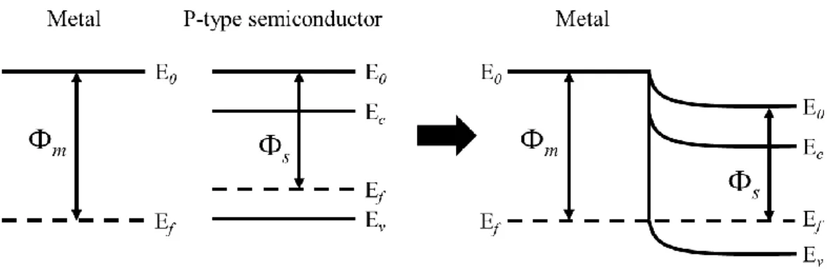
Take p-type semiconductor as example. When fermi-level (Ef) of metal is higher than
that of p-type semiconductor, indicating the work function of metal (Φm) is smaller than that
of p-type semiconductor (Φs). In thermal equilibrium, fermi-levels of both metal and
semiconductor are equal. To satisfy the continuity of vacuum energy (Eo), the energy band of
p-type semiconductor near junction should bend downward and forms a energy barrier. When
the additional forward bias voltage is applied on p-type semiconductor, the energy barrier
would decrease. As the applied forward voltage is large enough to overcome the energy
barrier, holes in semiconductor can transport to metal resulting in the increase of current.
Oppositely, the additional reverse bias voltage applied on semiconductor increases the energy
barrier which allows only little leakage current. In this case, the junction of metal and
semiconductor is called Schottky contact as shown in Fig. 2-2. On the other hand, when the
Fermi-level of metal is lower than Fermi-level of p-type semiconductor, work function of
11
in the junction of metal and semiconductor.Therefore, despite applying forward or reverse
bias voltage, the current is proportional to voltage and follows the Ohm’s law. As a result, this
situation is called ohmic contact as shown in Fig. 2-3.
The issue of the junction between organic materials and metal has been discussed for
decades. There are dipoles generated in the junction resulting in band bending. The
phenomenon of band bending can be reduced by using different organic materials. However,
there is still not a complete theorem to explain problems of the energy band between metals
and organic materials including small molecules and conjugated polymers. The band theorem
of inorganic semiconductors can be adopted to explain organic semiconductors. However, in
inorganic semiconductor, the electron affinity and ionic potential determine the conduction
band and valence band respectively, while, in organic semiconductors, lowest unoccupied
molecular orbital (LUMO) and highest occupied molecular orbital (HOMO) are used.
Furthermore, one organic semiconductor regarded as whether electron donor or electron
acceptor is depending on the distribution of LUMO and HOMO.
2.2 Charge Transportation of Organic Conjugated Polymer
As aforementioned, there isn’t a complete theory to demonstrate the carrier
transportation in conjugated polymers. In general, theories in electrical characteristics can be
12
2.2.1 Bulk Limited and Space Charge Limited Current Theories.
Bulk limited theory can be explained by space charge limited current. The space charge
limited current (SCLC) theory states the phenomenon that the current is controlled by the
semiconductor itself and there is no contact limited to affect the injection of carriers. For
adopting SCLC theory, the junction of metal and semiconductor should be ohmic contact, or
the junction barrier should be smaller than 0.2 eV due to the continuous increase of additional
bias.
The behavior of SCLC is found in the insulator by Rose and Lampert originally. They
also proved the Power-Law which states the current is proportional to voltage squared (I~V2).
The so-called SCLC indicates, in the devices, the injection rate of carriers is faster than the
transportation rate of carriers and the injected carriers would accumulate in semiconductor
forming space charges. The accumulated carriers then produce a built-in electric field to
prohibit carrier injection and reach a dynamic equilibrium. As a result, the SCLC refers to the
current dominated by space charges accumulated in organic semiconductor. This phenomenon
often occurs in materials with low carrier mobility. Therefore, organic materials are mostly
explained by SCLC theory. Actually, accumulation of carriers is a bad phenomenon in
light-emitting devices and solar cells. In light-emitting devices, carriers inject from electrode
to light-emitting layer. If the carrier-injecting rate is faster than carrier-transporting rate in
13
layer resulting in the decrease of efficiency. Besides, in solar cells, if carrier-dissociating rate
is so fast that carriers accumulate in dissociation region, it would also decrease the efficiency.
In general, the transporting length in organic material layer is longer than that in space
charge region. The diffusion current due to the difference of carrier concentration is negligible.
As a result only the drift current induced by electric field is considered. Under the
circumstance that there is no traps in semiconductor, for a single carrier transportation, the
current density and thickness (L) of devices follow Mott-Gurney square law [32]. The
following equation shows the relationship between current density and thickness where ε is
dielectric constant of semiconductor, L is thickness (or drift space between electrodes), V is
applied voltage across electrodes and μeff is effective carrier mobility (μeff is a function of
electric and temperature. In small electric field and fixed temperature, it can be regarded as a
constant.)
𝐽 =
9
8
𝜀 𝜇
𝑒𝑓𝑓𝑉
2𝐿
32.2.2 Thermionic Emission Theory and Tunneling Effect
The injecting amount of carriers suffers from junction limitation when the energy barrier
is larger than 0.3 eV. There are two theories to explain the phenomenon. One is thermionic
emission theory as the additional bias voltage is smaller than flat band voltage; the other is
14
(1) Thermionic emission theory
Thermionic emission theory states that carriers can overcome the energy barrier between
metal and organic semiconductor to transport due to the energy barrier between metal and
organic semiconductor is small enough or the additional bias voltage is small than the
flat-band voltage. The thermionic emission equation is as follows.
𝐽 = 𝐽
𝑆𝑇[ 𝑒𝑥𝑝 (
𝑒𝑉
𝑘𝑇
) – 1 ]
And
𝐽
𝑆𝑇= 𝐴
∗× 𝑇
2𝑒𝑥𝑝 (
−𝑒𝜙
𝐵𝑘𝑇
), 𝐴
∗≡
4𝜋𝑒𝑚
∗𝑘
2ℎ
3A* is Richardson constant, ϕB is the height of junction energy barrier, k is Boltzmann constant
and T is absolute temperature.
From above equations, we can find that JST ~ T2, indicating temperature has a great
impact on thermionic emission. Fig. 2-4 shows the schematic diagram of thermionic emission
theory.
(2) Tunneling effect
If the energy barrier near the junction of metal and semiconductor is too high, carriers
can hardly across the barriers. However, when the additional bias voltage is greater than flat
band voltage and reaches the conductive voltage, energy band of semiconductor layer can
therefore bend. As we can know, band width of energy barrier is proportional to band height
15
property, we can reduce the band width so that carriers can tunnel through the barrier and
enter semiconductor layer as shown in Fig. 2-5. In tunneling effect, there isn’t a specific
relationship between current and temperature. Besides, both of them are related to electric
field as below equation according to Fowler-Nordheim tunneling theory.
𝐽 ∝ 𝐸
2𝑒𝑥𝑝 ( −
𝐾
𝐸
) , 𝐾 = 8𝜋
√2𝑚
∗𝜙
𝐵33𝑞ℎ
E is intensity of electric field, m* is effective mass of carrier, ϕ
Bis height of
junction barrier energy, q is electron charge and h is Planck constant.
2.3 Operation of Space Charge Limited Transistor (SCLT)
Space charge limited transistor (SCLT) is developed from field effect transistor and this
concept is shown in Fig. 2-6. Because of the low carrier mobility of organic semiconductor,
enhancement of output current requires shortening the carrier channel length or raising the
operating voltage. However, the former requires expensive photolithograph techniques and
instruments, and the latter may lead to breakdown of devices. Both of them cannot fulfill our
requirement of operating at low voltage.
The channel length of a vertical SCLT depends on the thickness of semiconductor. The
thickness of semiconductor can be controlled by changing the solution concentration or the
speed of spin coater, indicating the channel length can be easily controlled. SCLT is a vertical
16
injected from emitter and are accepted in collector, while base is used to switch the current.
This device used ITO glass as substrate, organic materials are formed by spin-coating, and
electrodes are deposited by high vacuum thermal evaporator. Besides, the processes of porous
structures will be demonstrated in chapter 3.
SCLT, defined by the carrier injection direction, can be separated into bottom-injection
SCLT and top-injection SCLT. For bottom-injection SCLT, emitter is ITO and Al is collector;
for top-injection SCLT, emitter is MoO3/Al and collector is ITO as shown in Fig. 2-7.
Operation of SCLT is similar to vacuum tube theory. Additional bias at base forms
energy barriers in porous channel, and current can be controlled. In off state, there is a high
energy barrier in porous base, and carriers from emitter can hardly go through this barrier
resulting in little output current. In on state, the energy barrier in porous base is reduced or
even disappears, and carriers can reach collector leading to large output current. The
relationship between operation of SCLT and band diagrams is showed in Fig. 2-8.
2.4 Carrier Transport Mechanism of Metal-Oxide Semiconductors
In this section, the transport mechanism of amorphous indium gallium zinc oxide
(a-IGZO) is briefly demonstrated. The carrier transport mechanism and electronic structure in
an amorphous oxide semiconductor is similar to that of crystalline IGZO (sc-IGZO), and is
explained by percolation conduction through potential barriers in the vicinity of conduction
17
Zn2+ ions in the GaO+(ZnO)5 layer. The effective mass of a-IGZO was 0.34 me, which is almost
the same as that of crystalline IGZO. These results imply the electronic structure and carrier
transport mechanism in a- IGZO are similar to that in sc-IGZO, which would be associated with
the electronic structure of metal-oxide semiconductors in which electron transport paths are
made of spherical extended s orbitals and are not largely affected by local distortion of the
chemical bonds [33]. The intermediate region shown in Fig. 2-9 (1014 cm−3<Ne<Nth), the
carriers still need to flow over the potential barriers as EF is below Eth, leading to the thermally
activated percolation behaviors in µ and σ. When EF exceeds Eth at Ne>Nth, the carriers are not
affected by potential barriers anymore and exhibit the temperature-independent extended
mobility [34].
Each sub-element in the ternary material of a-IGZO film affects the parameters of TFT. It
is expected the increase of In concentration increases carrier concentration [25]. Because
indium atom is large, it is easy to lose electrons. The released electrons from In may be caught
by oxygen or move to the conduction band when a-IGZO film lacks of oxygen [35].
Therefore the carrier transportation can be enhanced. In addition, gallium in a-IGZO film
provides high stability for a-IGZO TFT [36]. Gallium in a-IGZO film can reduce electron
concentration and mobility. Ga was chosen because atomic radius of Ga is close to In. Hosono
et al. reported that Ga3+ in a-IGZO film tightly attracts oxygen due to high ionic potential
18
suppressed and oxygen ions escaping from a-IGZO film are induced [37]. Compared with
indium zinc oxide (IZO), the carrier concentration of a-IGZO (~1019 cm-3) is smaller than that
of IZO (~1021 cm-3) [37-39]. Besides, Ga also reduces the sensitivity of carrier concentration
to the variation of O2/Ar ratio [39], indicating Ga helps a-IGZO film to control carrier
concentration. However, the reduced mobility accompanies with the addition of Ga also.
Hosono et al. reported that oxygen molecules are doped to increase carrier concentration and
mobility in the presence of Ga in a-IGZO film [40]. Zinc in a-IGZO film was reported to
affect the crystallization of the thin film. Crystalline structure was reported with the ratio of
Zn in a-IGZO film lager than 65% [35]. The crystalline structure in a-IGZO film may cause
degradation of electrical characteristics while the uniformity was reduced by the disordered
grain boundaries.
2.5 Methods of Device Parameters Extraction
In this section, the extractions of the device parameters are discussed in details. The field
effect mobility, turn on voltage (Von), the on/off current ratio (Ion/Ioff), and the sub-threshold
swing (S.S) are extracted and assessed, respectively.
2.5.1 Mobility (μ)
Mobility is a measurement of the velocity of the carrier moving through a material. High
mobility allows high frequency response which is the time taken for the device to transfer from
19
amount of currents flows through the device. A large mobility indicates large output current.
The mobility in this study refers to the saturation mobility which is extracted from the
saturation region. The device is operated at drain voltage (VDS) of 20 V, since the threshold
voltage (VTH) is much lower than 20V. The saturation mobility is determined from the
transconductance (gm) defined as Eq. 2-1.
g𝑚 = [∂√I𝐷𝑆 ∂V𝐺𝑆]V
𝐷𝑆=const
Eq. 2-1
The drift component of drain current in saturation region is as Eq. 2-2.
I𝐷𝑆 =12μCWL(V𝐺𝑆 − V𝑇𝐻)2 Eq. 2-2
When the mobility is determined, IDS in Eq. 2-1 is replaced by Eq. 2-2.
gm= √WμC 2L
The saturation mobility (μsat) is solved as followed.
μsat = [2gm 2 W L𝐶 ] saturation
C is the capacitance of gate insulator, W is channel width, and L is channel length.
2.5.2 Turn-On Voltage (Von)
Turn-on voltage (Von) is defined as the gate voltage at which the drain current begins to
increase in a transfer curve. Von can directly characterize the gate voltage required to fully turn
off the transistor in a switching application.
2.5.3 Threshold Voltage (V
TH)
20
extract the threshold voltage from Eq. 2-3, the intercept point of the square-root of drain current
versus voltage when devices operate in saturation mode
√I𝐷𝑆 = √2LWμC(V𝐺𝑆 − V𝑇𝐻) Eq. 2-3
2.5.4 I
on/I
offCurrent Ratio
The Ion/Ioff (on/off) ratio represents the ratio between large turn-on current and small off
current. It is an indicator of how well a device will work as a switch. A large on/off current ratio
means there are enough turn-on current to drive the pixel and low off current to maintain in low
consumption.
2.5.5 Sub-Threshold Swing (S.S.)
Another important characteristic for device application is sub-threshold swing (S.S.). It is
a measurement of how rapidly the device switches from off state to on state. Moreover, the
sub-threshold swing also represents the interface quality and the defect density. Sub-threshold
swing is defined as followed. If we want to have a better performance TFTs, we need to lower
the sub-threshold swing.
S. S. = [ ∂V𝐺𝑆
21
Figures of Chapter 2
Fig. 2-1 The characteristics of current as a function of voltage. Both ohmic contact and
schottky contact are shown.
22
Fig. 2-3 Band diagram of ohmic contact.
Fig. 2-4 Schematic diagram of thermionic emission theory.
23
Fig. 2-6 Development of space charge limited transistor (SCLT) from field effect transistor.
Fig. 2-7 Structures of bottom-injection and top-injection SCLTs. (a) Bottom-injection SCLT,
emitter is ITO and Al is collector. (b) Top-injection SCLT, emitter is MoO3/Al and collector is
24
Fig. 2-8 The relationship between operation of SCLT and band diagrams. (a) On state of SCLT.
(b) Off state of SCLT.
Fig. 2-9 (a) The relationship between log(Ne) and activation energy (Ea). The straight line is
the result fitted to the exponential tail density of state model. (b) Schematic energy diagram
25
Chapter 3 Device Fabrication and Experiment Setup
3.1 Introduction
In this chapter, the fabrication processes, structures of devices and material analysis tools
used will be briefly introduced. During the processes, glove boxes filled with nitrogen were
used to prevent our devices from oxygen and vapor.
3.2 Space Charge Limited Transistor (SCLT) Sensor
In the section, the processes of vertical P3HT-based space charge limited transistor
(SCLT) sensors based on ITO glass substrate are demonstrated. The electrodes of SCLT are
emitter (E), base (B), and collector (C). Indium tin oxide (ITO) is used as emitter electrode,
while aluminum (Al) is used as base and collector electrodes. Active region of SCLT sensor is
1x1 cm2. Three-dimensional and two-dimensional SCLT sensor schematic diagrams are shown
in Fig. 3-1; a scanning electron microscope (SEM) image of SCLT is shown in Fig. 3-2. All the
fabrication steps were processed in glove box, except for glass substrate cleaning, ITO
patterning, and adherence of polystyrene (PS) balls. The flowchart of the fabrication
processes is showed in Fig. 3-3.
3.2.1 Glass Substrate Cleaning
Resistance and thickness of ITO on glass substrate were <7Ω and 200 nm. Before
26
cleaning was to remove particle and organic pollution on glass substrate. The followings were
procedures of glass substrate cleaning. First, Immerse the glass substrate in the streaming DI
water for 5 minutes: to remove particles. Second, put glass substrates into acetone (ACE)
under ultrasonic resonance for 10 minutes: to remove organic pollution. Third, immerse the
glass substrate in the streaming DI water for 5 minutes: to remove the residue of ACE. Fourth,
put glass substrates into isopropanol (IPA) under ultrasonic resonance for 10 minutes: to
remove organic pollution. Fifth, immerse the glass substrate in the streaming DI water for 5
minutes: to remove the residue of IPA. Sixth, use N2 to quickly blow off water drops remained
on the substrate to prevent spots of water. Finally, put glass substrates on the hot plate at 120℃
for 5 minutes to remove the residual moisture and then cool down to the room temperature.
3.2.2 ITO Patterning
To define the ITO electrodes, the shadow mask was used. The processes of ITO
patterning are as follow. First, put the cleaned ITO glass substrates on the hotplate at 170℃for
10 minutes. Then rapidly stick the negative photoresist (PR) onto the glass substrates once
ITO substrates leave the hot plate. Second, use the defined shadow mask and exposure to UV
lithography to define ITO patterns. Third, immerse the patterned substrates into K2CO3
solution of which the formula ratio is 50mg K2CO3 to 1000ml water for 50 to 80 seconds to
develop. After that, use DI water to clean, and then remove the residue PR by tissues. Fourth,
27
un-developed ITO, and then use DI water to clean. Finally, use 5 wt% sodium hydroxide
(NaOH) solution to remove PR and then use DI water to clean.
3.2.3 ITO Surface Planarization
Before forming insulator layer, Oxygen plasma at power of 100 W was used to treat the
ITO surface for 10 min. The purpose was to planarize the roughness of ITO surface.
3.2.4 Insulator Layer
Cross-linkable poly(4-vinyl phenol) (PVP) (8 wt.%) (Mw approx. 20000, Aldrich) and
cross-linking agent poly(melamine-co-formaldehyde) (PMF) were dissolved in propylene
glycol monomethyl ether acetate (PGMEA) with a PVP:PMF mass ratio of 11 : 4.
With 8wt% PVP solution, insulator layer was formed with PVP solution by spin-coating
on the patterned ITO glass substrate in the glove box. Then annealing at 200℃ for 1 hour
was used to make PVP form cross-link. The thickness of PVP after annealing was 200 nm
measured by Kosaka Laboratory Ltd., ET-4000.
3.2.5 Sacrificing Layer
A 1.5 wt% poly(3-hexylthiophene-2,5-diyl) (P3HT) (RR > 98.5%, Rieke Metals Inc.)
solution dissolved in chlorobenzene (CB) was used to form the sacrificing layer by
spin-coating at 5000 rpm for 30 seconds on the PVP layer in the glove box. After that, 200℃
28
3.2.6 Spin-Rinse
p-Xylene (4 drops) was used to spin-rinse the sacrificing layer by spin-coating at 7000
rpm for 60 seconds. After this process, it decreased the thickness of sacrificing layer by 10 nm
and increased the P3HT surface polarity.
3.2.7 Adherence of Polystyrene Balls
In this step, 0.4 wt% negatively charged polystyrene (PS) balls (Fluka-90517, diameter =
100 nm; Fluka-95581, diameter = 200 nm) solution dissolved in ethanol was used. After
spin-rinse, immerse the substrate into the 0.4 wt% PS balls solution for 90 seconds at first.
Then take the substrate out off the PS balls solution and use ethanol to clean. Finally, immerse
the cleaned substrate into boiling 220℃ IPA for 10 seconds, and then use nitrogen to blow the
substrate dry immediately.
3.2.8 Porous Base Electrode
With PS balls adhering to the sacrificing layer, 40 nm-thick Al served as the base
electrode (B) was deposited onto the substrate by thermal evaporation at the rate of 0.2 nm/s.
Then scotch tape (3M) was used to remove the PS balls covered with Al, and the left Al
comprised porous base electrode with revealed PVP insulator layer.
3.2.9 Vertical Channel
With porous base electrode as hard mask, oxygen plasma at 100 W for 10 minutes was
29
cylindrically vertical channels were formed.
3.2.10 Active Layer
A 350 nm active layer was composed of 4.5 wt% P3HT solution dissolved in CB by
spin-coating at 1500 rpm for 40 seconds. After spin coating, the substrate with P3HT-based
active layer was annealed at 200℃ for 10 minutes.
3.2.11 Porous Collector Electrode
After annealing the active layer, the substrates were treated with spin-rinse mentioned in
step (6) and adherence of PS balls mentioned in step (7) in order. With PS balls adhering to
the active layer, 40 nm-thick Al served as collector electrode (C) was deposited onto the
substrate by thermal evaporation at the rate of 0.2 nm/s. Finally, Scotch tape (3M) was used to
remove the PS balls covered with Al, and the left Al comprised porous collector electrode
with revealed P3HT-based active layer.
3.3 Amorphous IGZO TFT Hybrid Sensor
In this section, the fabrication of a-IGZO TFTs hybrid sensor including processes of
a-IGZO TFTs and capping of W18O49 as sensing layer are demonstrated. Two-dimensional
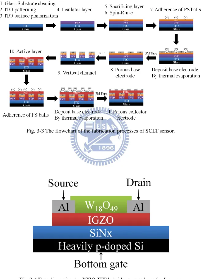
a-IGZO TFT hybrid sensor schematic diagram is shown in Fig. 3-4. The a-IGZO TFT here is
bottom gate top contact with heavily p-doped Si wafer as gate electrode, 100 nm silicon
nitride (SiNx) as gate dielectric, and 100nm Al as source and drain (S/D) electrodes. Channel
30
from Prof. Chi-Chuang Hu of National Tsing Hua University. A scanning electron microscope
(SEM) image of W18O49 is shown in Fig. 3-5.
3.3.1 Gate Dielectric Layer
A gate dielectric layer was deposited on a 6-inch heavily p-doped silicon wafer by low
pressure chemical vapor deposition (LPCVD) of National Nano Device Laboratories at 780℃
with gases of NH3 and SiH2Cl2. After deposition of SiNx, there was SiNx on both sides of the
p-doped silicon wafer. Reactive ion etching (RIE) was used to remove the SiNx on the back
side of the wafer and the revealed silicon was used as gate electrode. Process gases during
RIE were oxygen (O2) 5 sccm and tetrafluoromethane (CF4) 80 sccm. Besides, process pressure
and RF power were 15.0 Pa and 100W.
3.3.2 Substrate Cleaning
The 6-inch heavily p-doped Si wafer with SiNx on one side was split into 3×3 cm2
squares at first. Before deposition of active layer – IGZO film, the spilt substrates should go
through the standard clean composed of SC1 and SC2. The capability of SC1 and SC2 were to
remove microscopic particles and alkali metal ions on the surface of substrates respectively.
The first step of standard clean was using N2 to blow off macroscopic particles and flushing
the substrates with DI water for 5 minutes. Second, immerse substrates into SC1 solution for
10 minutes. SC1 solution was composed of ammonium hydroxide (NH4OH), hydrogen
31
1: 4: 20. Third, flush the substrates with DI water for 5 minutes. Fourth, immerse the
substrates into SC2 solution for 10 minutes. SC2 solution was composed of HCl, H2O2 as
oxidant, and 75 ~ 85 ℃ DI water with the formula: HCl: H2O2: H2O = 1: 1: 6. Finally, flush
the substrates with DI water for 5 minutes and use N2 to quickly blow off water drops
remained on substrates to prevent spots of water.
3.3.3 a-IGZO Film Deposition
Radio-frequency (rf) sputter and a 3-inch circular IGZO target (In: Ga: Zn: O = 1: 1: 1: 4
at%) were used to deposit 30 nm a-IGZO film at room temperature with rf power of 100W,
working pressure of 0.009 torr, and O2/(Ar+ O2) ratio of 0.098%. The pattern of a-IGZO was
defined by shadow masks.
3.3.4 Post-Annealing
After rf sputtering a-IGZO, 400℃ the substrates with a-IGZO film were post-annealed
at atmospheric pressure for 1 hour in a nitrogen furnace. The flow rate of nitrogen was 10 liter
per minute (L/m).
3.3.5 Source/Drain Deposition
100 nm Al was deposited as source/drain electrodes by thermal evaporator. Patterns of
source/drain were defined by shadow masks. The deposition was started at the pressure <
32
3.3.6 Sensing Layer Capping
Through step 1 to 5, the a-IGZO TFT was fabricated. Basing on a-IGZO TFT, W18O49
was capped as sensing layer. There were two methods to cap W18O49 which are drop and
spin-coating. They would be introduced respectively as follow.
Drop-coating
Before drop coating W18O49, a-IGZO TFTs were heated to 85℃. Then W18O49 solution
dissolved in ethanol was dropped onto the channel of a-IGZO TFTs. Finally, wait for the
evaporation of ethanol.
Spin-coating
Before spin-coating W18O49, a-IGZO TFTs, a-IGZO TFTs were irradiated by ultraviolet
(UV) rays for 5 minutes. After irradiation of UV rays, W18O49 were spun onto the channel of
a-IGZO TFTs at 500 rpm for 30 seconds. Then put the a-IGZO TFTs on 85℃ hotplate for 5
minutes to evaporate ethanol, and one layer of W18O49 was formed. By repeating the above
processes, more than one layer of W18O49 could be formed.
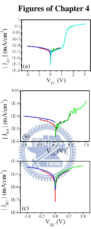
3.4 Micro-fluid Gas Sensing Measurement System
Gas sensing of SCLT sensor and a-IGZO TFT hybrid sensor is operated in the micro-fluid gas sensing measurement system shown in Fig. 3-6. A sensor was placed in a
micro-fluid sensing chamber containing an atmosphere of high purity (99.9999%) nitrogen (N2)
gas. For ammonia (NH3) gas sensing, an electrical syringe pump system was used to inject the
33
micro-fluid system; for nitric oxide (NO) sensing, the NO (10,000 ppm diluted in N2) gas was
directly injected into a tube to mix with the N2. The amounts of N2 and NO were controlled by
mass-flow controllers. Specific concentrations of NH3 and NO were obtained by adjusting the
injection speed of the syringe pump and by adjusting the flow rate of NO by the mass-flow
controller respectively. The sensing results were measured by Keithley 2400 connected to a computer.
3.5 Analysis Instruments
3.5.1 Current-Voltage Measurement Instruments
The instruments used for current and voltage measurement were Agilent E5270B and
Keithley 2400. Agilent E5270B was used to measure the electrical characteristics, while
Keithley 2400 was used during gas sensing.
3.5.2 Radio Frequency Magnetron Sputter
A radio frequency of 13.56 MHz is used to generate plasma. The generated plasma
creates ions to sputter the target material. Ions are accelerated towards the target by a negative
DC bias on the target. Generally, the RF sputtering is operated at the pressure of 0.05 torr to
improve the quality and the deposition rate of the deposited film. The quality of the film
deposited at the low pressure is increased due to the increase of mean free path contributing to
34
Figures of Chapter 3
Fig. 3-1 The three-dimensional and two-dimensional SCLT schematic diagrams.
35
Fig. 3-3 The flowchart of the fabrication processes of SCLT sensor.
36
Fig. 3-5 A scanning electron microscope (SEM) image of W18O49.
37
Chapter 4 Results and Discussion
4.1 Space Charge Limited Transistor (SCLT) Sensor
In this section, we demonstrate that the low switching swing of SCLT is critical to provide
high gas sensitivity. The lowest detectable ammonia concentration is 30 ppb for a
poly(3-hexylthiophene)(P3HT) SCLT. On the other hand, for P3HT OTFT with a conventional
bottom-gate structure, the detection limit to ammonia gas is larger than 1 ppm [41]. The high
sensitivity to ammonia achieved in this section enables the development of non-invasive breath
ammonia analysis for monitoring dysfunction of the human body [42].For such applications, a
portable and real-time ammonia sensor with a detection limit of 50 ppb is critical, but is still
challenging [42]. Besides, 30 ppm nitric oxide gas sensing were also demonstrated. Our
results may facilitate the development of low-cost point-of-care technology.
4.1.1 Characteristics of Porous SCLT
Before analyzing the experimental gas sensing response, the diode characteristics of the
SCLT with porous collector (porous SCLT), including EC, EB and BC diode, are shown in
Fig. 4-1 to confirm well injection of holes from emitter to collector and no leakage current
between EB and BC. During diode measurement, additional bias is added to the former
electrode while the latter one is grounded. EC diode as example, additional bias is added to
emitter and collector is grounded. Besides, the output characteristics, the collector current
38
Fig.4-2. With collector bias (VCE) as -2.4 V and -1.2 V, porous SCLT exhibits an on/off current
ratio as 4750 and 890, and a switching swing as 140 mV/dec. and 122 mV/dec., respectively.
Fig. 4-3 shows the transfer characteristics, the collector current density (JCE) as a function of
the base voltage (VBE), of porous SCLT. Two test gas sensing responses, the NH3 as the
e-doping gas and the NO as the e-dedoping gas, are investigated [43]. Gas sensing were
operated through micro-fluid gas sensing measurement system shown in Fig. 3.5-1.
4.1.2 Ammonia Sensing Results
In this section, results of NH3 sensing are demonstrated. The response sensitivity to NH3
is defined as follows:
Sensitivity= ∆J J0 =
JCE-JCE0
JCE0 Eq.4.1-1
where JCE and JCE0 are the collector current density exposed to NH3 for 200 second and the
one before NH3 exposure respectively from transfer characteristics (JCE-VBE curve).
Effect of Collector Voltage (VCE) on Sensitivity
The relationship between sensitivity and VCE is demonstrated at first. Fig. 4-4 shows a
plot of sensitivity to NH3 concentration with three different VCE bias conditions. The NH3
concentrations were ranged from 30 ppb to 1000 ppb; the VCE bias conditions are -1.2 V, -1.8
V and -2.4 V. With collector bias (VCE) as -1.2 V, porous SCLT exhibits the maximum
39
Carrier Injection Effect on Sensitivity
In this section, two structure of porous SCLT shown in were utilized to study the effect
of carrier injection. Because injection of holes is from emitter to collector, we can change the
injecting direction of holes, i.e. bottom-top or top-bottom, by using different metal as emitter
and collector. For bottom injection of holes, ITO and Al were used as emitter and collector
respectively. For top injection of holes, MoO3/Al and ITO were used as emitter and collector
respectively. Fig 4-5 shows a plot of sensitivity as a function of NH3 concentration with
different injection of holes and the NH3 concentrations were ranged from 10 ppb to 1000 ppb.
We can find that the response of bottom injection is higher than top injection. The mechanism
is still unknown to explain the better sensitivity of bottom injection structure. However, as
shown in Fig. 4-6, it is supposed that hole concentration in the bulk area (the exposing area) of
P3HT is higher for top injection than that for bottom injection, indicating the proportion of
holes reacted with NH3 is relatively smaller than bottom injection which has less hole
concentration in bulk region. As a result, the response of bottom injection is higher.
Effect of Base Voltage (VBE) on Sensitivity
Fig. 4-7(a) shows a plot of JCE-VBE, representing the porous SCLT’s sensing response to
NH3. VCE was fixed as -1.2 V and the NH3 concentrations were ranged from 30 ppb to
1000 ppb. The response of the switching region (VBE = -0.4 V to 0 V) of JCE-VBE plot is shown
40
NH3 acts as electron doping (e-doping) agents, increasing NH3 concentration indicates
increasing e-doping concentration in P3HT which turns out to be the increase of the potential
barrier. Therefore, a more negative base potential is required to lower down the channel
potential barrier and to turn on the transistor. The sensing sensitivities △J/J0 as a function of
VBE for various NH3 concentrations are plotted in Fig. 4-8(a). We found that the sensitivity was
strongly dependent on VBE, and that the maximum sensitivity occurred in the switching zone
(-0.5 V < VBE < 0 V). For NH3 concentrations of 30 ppb, 100 ppb, and 1000 ppb, the maximum
sensitivities measured at VBE = -0.2 V and VCE = -1.2 V are -0.09, -0.23, and -0.56, respectively.
As shown in Fig. 4-8(b), a power law relationship is found between the maximum sensitivity
and NH3 concentration, indicating that the proposed NH3 sensor is particularly sensitive in
low-concentration regime (i.e. 30 ppb to 1000 ppb). Besides, we also compare sensitivity of a
SCLT sensor with that of a diode sensor (previous results by M. Z. Dai) in Fig. 4-8(b). For
diode sensor, ITO and porous Al were used as electrodes, and 300 nm P3HT acted as active
layer and sensing layer. It shows that SCLT sensor exhibits a better sensitivity to NH3.
However, the mechanism to explain the difference between SCLT and diode sensors is still
unclear.
SCLT Bias Stress on Sensing Response
As aforementioned, effect of NH3 on porous SCLT makes JCE-VBE curves shift to the left