Low Power Full-Search Block-Matching Motion
Estimation Chip for H.263+
Jun-Fu Shen , Liang-Gee Chen , Hao-Chieh Chang and Tu-Chih Wang DSPAC Design Lab, Department of Electrical Engineering
National Taiwan University Taipei, Taiwan. R.O.C.
ABSTRACT
In this paper, a low power full-search block matching (FSBM) motion estimation design for the H.263+ low bit rate video coding was proposed. The features of H.263+ such as half-pixel precision and some advanced modes (advance prediction mode, PB-frame mode and reduced resolution update mode) are taken into consideration. This architecture can deal with different
block size and searching range in a single chip without
any latency. We use a 1-D and 2-D mixed architecture to
fulfill this goal. To achieve the purpose of low power and reduce the design period, we use dual supply voltage levels in this chip. This chip is realized by
TSMC 0.6um single-poly triple-metal CMOS
technology. The operation frequency is set at 60MHz to meet the requirement of the real time processing in the reduced resolution update mode in H.263+. The power consumption is 424mW at 60MHz and the throughput is 36 frames per second with CIF format at 60MHz.
Keyword VLSI architecture, Motion Estimation, Videohmage
coding
1.
INTRODUCTION
Since the multimedia applications become more and more popular, the bandwidth of communication network has become insufficient obviously. In last ten years, there were many video and audio standards proposed to reduce the bitrate and improved the quality during transmission time. ITU-T announced the H.263 version
2 [l] called H.263+ to meet these requirements. For
H.263+ standard, there are additional sixteen negotiable advanced modes and motion estimation still plays a very important role. Although there are several studies on motion estimation architectures, [2-71, they can not meet the computation requirements of H.263+. Besides,
because of the widespread application of the portable
and wireless communication device, it can't be ignored the low-power issue, especially for the motion estimation, while the higher computation leads to more
power consumption. To prolong the using period
between the battery recharging, it is a trend to develop the low-power motion estimation architecture.
Therefore, this paper proposed a low-power FSBM motion estimation ASIC design for the latest H263+ video standard. The architecture overview is described in section 2. And the architectures of integer-pixel
precision unit (IU) and half-pixel precision unit (HU)
are depicted in section 3 and 4. Section 5 shows the chip
implementation and simulation results. Finally, a
conclusion is given in section 6.
2. ARCHITECTURE OVEWVIEW
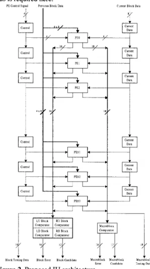
Figure 1 is the overview of the whole architecture. The IU and HU are used to calculate the MAE in integer- pixel and half-pixel precision individually. In IU, we use
64 processing elements (PE) that is a tradeoff between
speed and area. The current and previous frame data come from the off chip memory and don't include in our
architecture. To achieve the 100% PE utilization during
the working time, we use four input ports for the previous block data and one input port for the current block data in IU. In HU, the previous block data and the current block data share the same port because of the low requirement of the input bandwidth.
,I M a l * ,I R..., ""I S*! i l L " l l i i "I I l l *
Figure 1. Architecture overview
0-7803-5471 -0/99/$10.0001999 IEEE
In the output block, we use an identical 30-bit register to output the motion vector and the minimum absolute
error for IU and HU sequentially to reduce the number
of output pad.
3.
ARCHITECTURE FOR INTEGER-
PIXEL PRECISION UNIT
Figure 2 is the proposed IU architecture, the current
block data is reused by using the 64 8-bits shift registers in the right side, and the previous block data broadcasts to each PE from the four 8-bits buses. The MAE in each PE is transmitted to the macroblock comparator and the block comparator through the 18-bits bus and the 16-
bits bus. In Figure 2, there are 64 4-bit shift registers
placed in the left side and these registers are used to store the control signal. Using these registers, the design of control signal flow becomes much easy and no global bus is required here.
PE Coolrol Signal PI Control I 4
y
I :/,
4
4 I ,-I PE1 4 I I 4 4 44
Block T111ing Data Block Error Block Candidate M#crobiock Ms!oblork Marroblack
Enor Candidalr Tcaling Dsts
Figure 2. Proposed IU architecture
A. PE Architecture
Figure 3 is the PE cell we proposed here. The major
difference from other PE architecture proposed before is marked as the gray blocks, and those registers that named as G register means that the clock of this register is gated control.
The function of gray part B that we call block
accumulator is to accumulate the MAE of a block. To
reduce the power consumption in each PE, we use gated clock control in the block accumulator. The gray part C that we call macroblock accumulator is the additional part from general PE architecture. It is used to accumulate the MAE of macroblock. In the same
candidate position, the MAE of the macroblock is the
summation of the MAE of four blocks that belong to
this macroblock.. So the data in each block accumulator
can be reused in the macroblock accumulator one after another. For low power consideration, it needn't use the same clock period in block accumulator as in
macroblock accumulator. It only needs to use a 64 time
clock period in macroblock accumulator to reduce the
activity rate in the 18 bits register B and 16 bits register C.
B. Variable block size and searching range
consideration
Considering the variable block size requirement, if we
need the MAE with 8 X 8 block size, the PE just send
the MAE in the block accumulator to the comparator. If
we need the MAE with 16 X 16 block size, the
macroblock accumulator is used. For the 32 X 32 block
size, to achieve no latency in the working time, we
divide the 3 2 x 3 2 block into four 16X 16 sub-blocks.
At Every 256 clock cycles, the block accumulator in
each PE calculate the MAE in the 8 X 8 sub-block. After
repeating four times, the MAE of a 32 X 32 block has
been finished and is sent to the comparator.
To achieve the variable searching range consideration,
we use the searching range partition strategy. For a 32 X
32 searching range, we divided it into sixteen 8 X 8 sub-
searching ranges. And each 64 clock cycles the PE array
deals with only one sub-searching range. For a 64 X 64
searching range, we divide the whole searching range
into 64 8 X 8 sub-searching ranges. Because we use 64
PES architecture and 2-D searching method, we can
easily achieve the variable searching range just divide
the whole searching into several 8 X 8 sub-searching
range and each time processing only one sub-searching range as mentioned above. And the data flow in each sub-searching range is still the same, we still has no
latency between each sub-searching range.
4.
ARCHITECTURE FOR HALF-PIXEL
PRECISION UNIT
The HU is composed with an interpolation pixel generator, a processing element and a comparator as
shown in Figure 4. The input of the current block data
and the previous block data share the same input port because of the low demand of the input bandwidth.
Figure 5 is the architecture of the interpolation pixel
generator in HU we proposed. In this architecture, we
use only two adders and seven registers. The G register means that the clock of this register is gated control. We use only one 8-bit input port because of the low input bandwidth. Figure 6 and Table 1 shows the data flow in the interpolation pixel generator. The input data stream
is C, PO, Pl;.. ., P8, the output data stream is HO, H1,
H2;.-,H7, and the current block pixel C is stored in the register A during the interpolation cycle. From Table 1 we see that for an interpolation cycle, it needs eleven
clock cycles. So for a 8 X 8 block size, it needs 11 X 8 X
cycles. This number is still smaller than the clock cycles we need in IU. We use only one FE in HU. But we have to calculate nine candidates during a block matching, we use nine shift
partial absolute error in each ca
HU.
Table 1. Interpolation pixel generator data flow
5.
IMPLEMENTATION
To reduce the design period and meet the low-power requirement, we use full-custom and cell-based hybrid design in this work. In the PE array, we use full-custom design because of its large area and high power consumption. And we use 2.5 volts supply voltage in it. In the other modules such as controller, we use cell- based design to reduce the design period. Since the cell library we used is only support 5-volt supply voltage, we use dual supply voltage levels in our chip.
To minimize the power consumption in the shift registers, we use the TSPC register proposed in [8] here. Because there are two voltage levels in our chip, we need a voltage swing circuit. For the low-to-high level converter, we use the low-to-high level converter proposed in [9]. This chip is implemented with TSMC 0.6um single-poly triple-metal technology and uses the COMPASS cell library. Figure 7 shows the physical layout view with the whole chip. The detail description
of the chip specification is listed in Table 2.
Table 2. Chip specification
6.
COWCEEJS~ION
In this paper, we proposed a low-power FSBM motion H.263+ such as half-pixel precision, AP’ mode, PB mode, and RRU mode. By the properly design for the PE cell, this architecture can fit variable block size and searching range requirement in a signal chip and still consumes less power.
This chip was implemented by TSMC 0.6um single- poly triple-metal technology. In the circuit level, we used TSPC register to minimize the power consumption in shift registers and dual voltage levels to realize the hybrid design strategy. From the simulation result, this chip can work at 60MHz and the power consumption is 334mw. It is enough to the real time requirement for RRU mode in H.263+ with QCIF picture format.
architecture thab supports some featu
7.
REFERENCE
ITU-T Recommendation H.263 version 2: “Video coding for low bit rate communication,” Sep. 1997.
G. Fujita, T.Onoye, and I. Shirakawa, “A New
Motion Estimation Core Dedicated to H.263 Video Coding,” IEEE Int. Symp. Circuits Syst., vol. 3, pp. 1161-1164, June 1997.
S. H. Nam and M. K. Lee, “Flexible VLSI Architecture of Motion Estimator for Video Image
r41
[51
[61
,lpul Dall
-
BApplication," IEEE Trans. Circuits Syst., vol. 43, no. 6, pp. 467-470, June 1996.
K. M. Yang, M. T. Sun, and L. Wu, "A Family of VLSI Designs for the Motion Compensation Block-Matching Algorithm," IEEE Trans. Circuits
Syst. Video Technol., vol. 36, no. 10, pp1317-
1325, Oct. 1989.
M. J. Chen, L. G. Chen, T. D. Chiueh, and Y. P.
Lee, "A New Block-Matching Criterion for Motion Estimation and its Implementation," IEEE
Trans. Circuits Syst. Video Technol., vol. 5 , no. 3,
pp. 231-236, Jun. 1995.
L. G. Chen, W. T. Chen, Y. S. Jehng and T. D.
Chiueh, "An Efficient Parallel Motion Estimation Algorithm for Digital Image Processing," IEEE
Trans. Circuits Syst. Video Technol., vol. 1, no. 4,
Pixel 8 , ErCO' ,' b Y O t l D O V I C l O i
+
Comparator Interpolation Processing i s , b ErrorPixel Generator Element
pp.378-395, Dec. 1991.
Y. K .Lai, L. G. Chen, H. T. Chen, M. J. Chen, Y.
P. Lee and P. C. Wu, "A Novel Video Siganl
Processor with Programmable Data Arrangement and Efficient Memory Configuration," IEEE Trans. Consumer Electronics, vol. 42, no. 3, pp.526-534, Aug. 1996.
J. Yuan and Svensson C., "High-speed CMOS circuit technique," IEEE J. Solid-state Circuits, vol. 24, no. 1, pp. 62-70, Feb. 1989.
J. S. Caravella and J. H. Quigley, "Three volt to five volt interface circuit with device leakage limited dc power dissipation," IEEE ASIC Intern. Conf. and Exhibit, Rochester, NY, pp. 448-451, Sep. 1993.
[7]
[8]
[9]
Figure 6. Input pixels and the half-
Figure 3. Proposed PE architecture pixel positions
Figure 4. Proposed HU architecture
Figure 5. Interpolation pixel generator Figure7.Whole chip physical layout