Enhancement in the efficiency of light emission from silicon
by a thin Al
2O
3surface-passivating layer grown
by atomic layer deposition at low temperature
M. J. Chen,a兲Y. T. Shih, M. K. Wu, and F. Y. TsaiDepartment of Materials Science and Engineering, National Taiwan University, Taipei, Taiwan 106, Republic of China
共Received 12 September 2006; accepted 20 December 2006; published online 15 February 2007兲 Thin Al2O3 surface-passivating layers grown by atomic layer deposition at 100 ° C were demonstrated to be instrumental in producing efficient light emission from silicon. External quantum efficiency up to 1.3⫻10−4 was observed from silicon metal-insulator-semiconductor light-emitting diodes with a 5 nm Al2O3 surface-passivating layer as the insulator, which is more than tenfold that from similar devices with a 5 nm SiO2 insulator layer thermally oxidized at 1000 ° C. Anomalous temperature dependences of the photoluminescence intensities and spectra at low temperatures indicate the presence of bound excitonic traps at the Al2O3/ Si interface. The enhanced light emission may be attributed to the temporary capture of excitons by the interfacial bound excitonic traps, which effectively reduces nonradiative recombination. © 2007 American Institute of Physics.关DOI:10.1063/1.2464190兴
Since silicon is the most important material for ultra-large-scale-integration 共ULSI兲 circuits, the monolithic inte-gration of microelectronics and optoelectronics in a single silicon chip has gathered considerable attentions in recent years.1–17Few silicon-based light-emitting sources, however, have been able to realize practical applications on optoelec-tronics. In bulk silicon, where radiative recombination of car-riers is a phonon-assisted process due to the indirect band gap, nonradiative recombination proceeds much faster than radiative recombination, causing most carriers to recombine nonradiatively. This leads to a very low quantum efficiency of light emission from bulk silicon 共⬃10−6兲. Therefore, reducing nonradiative recombination of carriers is deemed a promising approach to increase the light-emission efficiency from silicon.
In order to achieve silicon-based light-emitting devices with high luminescence efficiency, nonradiative recombina-tion of carriers has to be reduced to a very low level, both in the bulk and at the surface. Nonradiatve recombination in the bulk can be minimized by using high-quality silicon sub-strates, such as those grown by the float-zone共FZ兲 or mag-netically confined Czochralski 共MCZ兲 process.15 Nonradia-tive recombination at the surface can be suppressed by passivating the surface. The silicon surfaces are convention-ally passivated by thermconvention-ally oxidized SiO2.15The high pro-cessing temperatures 共usually ⬎700 °C兲 required to form thermal SiO2, however, prohibits thermal SiO2from applica-tions requiring low-temperature processing. Another way to grow high-quality passivation layers on silicon surface is to use atomic layer deposition 共ALD兲.18,19 ALD is a surface-controlled layer-by-layer process for depositing thin films with atomic-layer accuracy. During a typical ALD process, an excess of each precursor is alternatively supplied to satu-rate the surface sites, resulting in self-limiting film growth.
Owing to its self-limiting characteristics, ALD offers many advantages, including accurate and facile thickness control, excellent conformality, abrupt interfaces, high uniformity over a large area, good reproducibility, dense and pinhole-free structures, and low deposition temperatures, etc.18,19The high quality of ALD films is manifested by the prominence of ALD high-K dielectrics, such as Al2O3 and HfO2, which are poised to replace SiO2 in the future-generation silicon ULSI circuits.20 In this study we used ALD to grow thin Al2O3 films as the insulator layer in metal-insulator-semiconductor 共MIS兲 light-emitting diodes 共LEDs兲 on sili-con at a low temperature of 100 ° C. The ALD Al2O3 insu-lator serves as a surface-passivating layer to reduce nonradiative recombination of carriers at the silicon surface, thereby enhancing the light-emission efficiency from silicon. The ALD Al2O3 film was deposited on the silicon sub-strate held at 100 ° C using alternating pulses of Al共CH3兲3 共trimethylaluminum 共TMA兲, the Al precursor兲 and H2O共the oxygen precursor兲 in a N2 carrier gas flow. The deposited thickness was 5 nm. n-type共100兲 silicon substrates with re-sistivity of 0.1– 1⍀ cm and grown by FZ method were used in this study. Prior to ALD, the silicon substrates were cleaned in a dilute HF solution to remove the native oxide. The ALD process consisted of a number of identical cycles, each of which contained the following sequence: TMA, 0.1 s→N2 purge, 5 s→H2O, 0.1 s→N2 purge, 5 s. Each ALD cycle deposited⬃1 Å of Al2O3. The thickness of the deposited Al2O3film was controlled by the number of ALD cycles. The gate electrodes of MIS LEDs were prepared by thermally evaporating aluminum on the Al2O3-deposited sili-con substrates. The aluminum gate electrodes were circular, each with an area of 1.78⫻10−2cm2. Aluminum was also deposited on the backside of the silicon substrates as another electrode of the MIS LEDs. To investigate the light-emission efficiency from silicon with different surface-passivating lay-ers, we also fabricated the MIS LEDs with the gate dielectric a兲Electronic mail: [email protected]
JOURNAL OF APPLIED PHYSICS 101, 033130共2007兲
0021-8979/2007/101共3兲/033130/4/$23.00 101, 033130-1 © 2007 American Institute of Physics
replaced by a 5 nm SiO2layer grown by thermal oxidation at 1000 ° C on the same type of silicon substrate.
The 5 nm Al2O3 or SiO2 films in the MIS LEDs were thin enough to allow significant amount of carriers to tunnel through. Figure 1 shows the current versus voltage 共I-V兲 curve of the MIS LED with Al2O3 as the gate dielectric, which shows a rectifying characteristic. The electrolumines-cence共EL兲 spectrum at room temperature is shown in Fig.2. Under a positive gate voltage, an accumulation layer of ma-jority electrons is formed near the Al2O3/ Si interface. The electrons tunnel from the silicon to the gate electrode, while the holes tunnel in the opposite direction. After relaxing to the valence band edge, the holes may radiatively recombine with the accumulated electrons to emit light from the Al2O3/ Si interface. The spectral position of the EL signal around 1.07 eV indicates that the light emission resulted from the transverse optical 共TO兲 phonon-assisted interband transition in silicon.21
Figure3shows the room-temperature optical power ver-sus injection current 共L-I兲 curves of the MIS LEDs with Al2O3 or SiO2 as the gate dielectric. We used an InGaAs p-i-n diode placed near the aluminum gate electrode to de-tect the optical power of the emitted light. The external quan-tum efficiency for the Al2O3 devices was measured to be
1.3⫻10−4. Since the luminescence was almost blocked by the aluminum gate electrode, only the light emission from the periphery of the device was measured. The internal quan-tum efficiency was, hence, estimated to be on the order of 10−3. The external quantum efficiency for the SiO
2 devices, on the other hand, was only 5.8⫻10−6. The EL efficiency of the Al2O3 devices was more than one order of magnitude higher than that of the SiO2 devices. This indicates that, compared to the thermal SiO2 films grown at 1000 ° C, the ALD Al2O3films grown at a temperature as low as 100 ° C were more effective in passivating the silicon surface and reducing nonradiative recombination.
The difference in the carrier recombination mechanisms between Al2O3- and SiO2-passivated silicon surfaces were investigated by measuring the temperature dependence of photoluminescence共PL兲 from these surfaces. Figure4shows the PL intensities as a function of temperature for both types of samples. Note that these samples had no metal gate elec-trodes. With the SiO2 sample, the PL intensity decreased rapidly when the temperature rose from 10 to 300 K, as a result of thermal activation of nonradiative recombination. The PL intensity of the Al2O3 sample, on the contrary, in-creased as the temperature rose from 10 to 110 K, and then decreased slowly with increasing temperature above 110 K. The PL intensity of the Al2O3 sample was greater than that of the SiO2sample at temperatures above 60 K. This anoma-FIG. 1. I-V curve of the silicon MIS LED with a 5 nm Al2O3layer as the
gate dielectric.
FIG. 2. Room-temperature EL spectrum of the silicon MIS LED with a 5 nm Al2O3layer as the gate dielectric.
FIG. 3. Room-temperature L-I curves of the silicon MIS LEDs with ALD Al2O3or thermal SiO2as the gate dielectric.
FIG. 4. Temperature dependence of the PL intensity for the silicon sub-strates with an ALD Al2O3or thermal SiO2surface-passivating layer.
033130-2 Chen et al. J. Appl. Phys. 101, 033130共2007兲
lous temperature dependence of PL intensity may be attrib-uted to the bound excitonic traps at the Al2O3/ Si interface.16,17,21
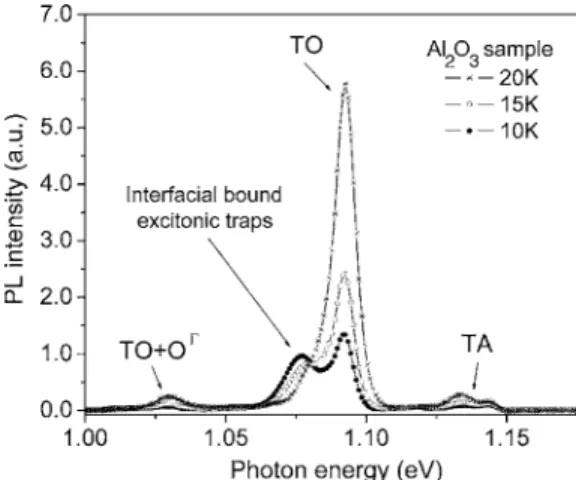
Figure5shows the PL spectra of the Al2O3sample at 10, 15, and 20 K, respectively. The PL spectra of the SiO2 sample at 10, 50, and 100 K are also shown in Fig. 6 for comparison. The PL spectra of both samples contain three peaks, corresponding to the two-phonon共TO+O⌫兲, TO, and transverse acoustic 共TA兲 phonon-assisted transitions, respectively.21 The spectra of the Al2O3 sample, however, show an additional peak at energy lower than the main TO peak. This spectral peak may be attributed to the interfacial bound excitonic traps at the Al2O3/ Si interface. As the tem-perature increases from 10 to 20 K, this spectral peak gradu-ally diminishes, while the main TO peak significantly inten-sifies. The intensity of the main TO spectral peak continues to increase with temperature up to 110 K. On the contrary, the TO spectral peak of the SiO2 sample decreases rapidly with increasing temperature, as shown in Fig.6. Considering that no spectral signal corresponding to bound excitonic
traps appeared in the PL spectrum of the SiO2 sample at 10 K, the anomalous increase in the main TO spectral peak with temperature, as shown in Fig.5, may be associated with the decrease of the spectral signal from the interfacial bound excitonic traps in the Al2O3sample.
The anomalous temperature dependence of PL intensity of the Al2O3 sample may be explained as follows. At low temperatures, excitons were bound in the traps at the Al2O3/ Si interface. When the temperature increased from 10 to 110 K, the excitons were thermally ionized to escape from the traps, raising the concentration of free excitons, which in turn increased the PL intensity. In other words, our observed increase in PL intensity with temperature may have been caused by thermal dissociation of bound excitons. At temperatures above 110 K, the PL intensity dropped, as non-radiative recombination became increasingly activated. The activation energies of the nonradiative recombination states and of the dissociation of bound excitons to free excitons, Enr and Et, respectively, were obtained by fitting the experimen-tal data using the following expression:21,22
I共T兲 = I0
关1 + gT3/2exp共− E
nr/kBT兲兴关1 + c/关1 + bT3/2exp共− Et/kBT兲兴兴
, 共1兲
where I is the PL intensity, T is the temperature, I0is the PL intensity at low temperature, kB is the Boltzmann constant, and g, c, and b are parameters independent of temperature. An efficient nonradiative recombination process has a small value of activation energy, Enr. The solid lines in Fig.4 are the fitted curves using expression共1兲. For the Al2O3sample, the activation energy of the dissociation of bound excitons to free excitons, Et, was calculated to be 9.4 meV, which agrees with the thermal energy at the temperature, 110 K, at which the PL intensity in Fig. 4 showed the maximum. Enrof the Al2O3sample共70 meV兲 is much larger than that of the SiO2 sample 共12 meV兲, indicating that the nonradiative
recombi-nation states were less thermally active and less efficient for the Al2O3sample. The bound excitonic traps at the Al2O3/ Si interface captured the excitons and effectively prevented them from decaying quickly through the nonradiative recom-bination states, and thus were responsible for the higher light-emission efficiency at room temperature.
In summary, light emission from silicon with a thin Al2O3surface-passivating layer deposited by ALD at a tem-perature as low as 100 ° C was studied. The room-temperature EL with external quantum efficiency up to 1.3 ⫻10−4was demonstrated for silicon MIS LEDs with an ALD Al2O3 layer as the gate dielectric, which is more than
ten-FIG. 5. PL spectra of the silicon substrate with an Al2O3surface-passivating
layer at 10, 15, and 20 K. FIG. 6. PL spectra of the silicon substrate with a SiOlayer at 10, 50, and 100 K. 2surface-passivating
033130-3 Chen et al. J. Appl. Phys. 101, 033130共2007兲
fold that from similar devices with a SiO2 insulator layer thermally oxidized at 1000 ° C. The low-temperature PL spectra of the Al2O3-passivated sample contain a peak that may be assigned to bound excitonic traps at the Al2O3/ Si interface. The dissociation of bound excitons to free excitons may have been responsible for the observed anomalous tem-perature dependence of PL intensity. The enhanced light emission from the Al2O3-passivated silicon MIS LEDs was attributed to the temporary capture of the excitons by the interfacial bound excitonic traps, which effectively sup-pressed nonradiative recombination. Our results show that the Al2O3films grown by ALD at low temperature served as good surface passivation layers for silicon LEDs. The low deposition temperatures required for ALD will be useful in the surface passivation of thermally fragile substrates and nanostructures.
This work is supported in part by the National Science Council, Taipei, Taiwan, Repulic of China under the Contract No. NSC 94-2112-M-002-019.
1R. A. Soref, Thin Solid Films 294, 325共1997兲.
2D. J. Lockwood, Light Emission in Silicon: From Physics to Devices 共Academic, New York, 1998兲.
3L. Pavesi, S. V. Gaponenko, and L. Dal Negro, Towards the First Silicon
Lasers共Kluwer Academic, Dordrecht, 2003兲.
4L. Pavesi, Mater. Today 8, 18共2005兲.
5L. Pavesi, L. Dal Negro, C. Mazzoleni, G. Franzo, and F. Priolo, Nature 共London兲 408, 440 共2000兲.
6L. Tsybeskov, K. L. Moore, D. G. Hall, and P. M. Fauchet, Phys. Rev. B 54, R8361共1996兲.
7Z. H. Lu, D. J. Lockwood, and J. M. Baribeau, Nature共London兲 378, 258 共1995兲.
8H. A. Atwater, G. I. Bourianoff, and R. J. Walters, Nat. Mater. 4, 143 共2005兲.
9L. T. Canham, Appl. Phys. Lett. 57, 1046共1990兲.
10J. Palm, F. Gan, B. Zheng, J. Michel, and L. C. Kimerling, Phys. Rev. B 54, 17603共1996兲.
11S. Coffa, G. Franzo, and F. Priolo, Appl. Phys. Lett. 69, 2077共1996兲. 12S. G. Cloutier, P. A. Kossyrev, and J. Xu, Nat. Mater. 4, 887共2005兲. 13H. Rong, R. Jones, A. Liu, O. Cohen, D. Hak, A. Fang, and M. Paniccia,
Nature共London兲 433, 725 共2005兲.
14W. L. Ng, M. A. Louren, R. M. Gwilliam, S. Ledain, G. Shao, and K. P. Homewood, Nature共London兲 410, 192 共2001兲.
15M. A. Green, J. Zhao, A. Wang, P. J. Reece, and M. Gal, Nature共London兲 412, 805共2001兲.
16J. M. Sun, T. Dekorsy, W. Skorupa, B. Schmidt, and M. Helm, Appl. Phys. Lett. 83, 3885共2003兲.
17J. M. Sun, T. Dekorsy, W. Skorupa, B. Schmidt, A. Mücklich, and M. Helm, Phys. Rev. B 70, 155316共2004兲.
18M. Ritala and M. Leskelä, Nanotechnology 10, 19共1999兲.
19L. Niinistö, J. Päiväsaari, J. Niinistö, M. Putkonen, and M. Nieminen, Phys. Status Solidi A 201, 1443共2004兲.
20M. Houssa, High k Gate Dielectrics共Taylor & Francis, London, 2003兲. 21G. Davis, Phys. Rep. 176, 84共1989兲.
22J. I. Pankove, Optical Processes in Semiconductors共Dover, New York, 1971兲.
033130-4 Chen et al. J. Appl. Phys. 101, 033130共2007兲