行政院國家科學委員會專題研究計畫 成果報告
後段製程材料於電阻式記憶體元件與材料之研究(I)
研究成果報告(精簡版)
計 畫 類 別 : 個別型 計 畫 編 號 : NSC 98-2221-E-151-058- 執 行 期 間 : 98 年 08 月 01 日至 99 年 07 月 31 日 執 行 單 位 : 國立高雄應用科技大學電子工程系 計 畫 主 持 人 : 劉志益 計畫參與人員: 碩士級-專任助理人員:莊子儀 報 告 附 件 : 出席國際會議研究心得報告及發表論文 處 理 方 式 : 本計畫涉及專利或其他智慧財產權,2 年後可公開查詢中 華 民 國 99 年 09 月 30 日
行政院國家科學委員會補助專題研究計畫
■ 成 果 報 告
□期中進度報告
後段製程材料於電阻式記憶體元件與材料之研究(I)
計畫類別:■ 個別型計畫 □ 整合型計畫
計畫編號:
NSC 98-2221-E-151 -058
執行期間: 98 年 8 月 1 日至 99 年 7 月 31 日
計畫主持人: 劉志益
共同主持人:
計畫參與人員: 專任研究助理莊子誼
成果報告類型(依經費核定清單規定繳交):■精簡報告 □完整報告
本成果報告包括以下應繳交之附件:
□赴國外出差或研習心得報告一份
□赴大陸地區出差或研習心得報告一份
■出席國際學術會議心得報告及發表之論文各一份
□國際合作研究計畫國外研究報告書一份
處理方式:除產學合作研究計畫、提升產業技術及人才培育研究計畫、列
管計畫及下列情形者外,得立即公開查詢
■涉及專利或其他智慧財產權,□一年■二年後可公開查詢
執行單位:
國立高雄應用科技大學
中 華 民 國 99 年 9 月 29 日
一、中文摘要
本實驗利用磁控濺鍍法沉積氧化銅薄膜於白金基板上,最後以熱蒸鍍系統配合金屬遮罩 定義上電極,完成金屬/絕緣層/金屬結構,並針對材料特性與電性方面做分析。在物性 方面利用掃描式電子顯微鏡(SEM)觀察薄膜表面形貌與觀測截面影像,並使用低掠角X 光繞射(GXRD)分析薄膜晶相。在電性方面探討元件其電阻切換特性、電流傳導機制、
記憶時間測試等特性,最後利用二氧化矽薄膜製作出SiO2/CuxO雙層結構,進而針對兩
者探討單層與雙層結構之差異比較。 關鍵字: 電阻式記憶體、氧化銅、二氧化矽
英文摘要
The CuxO and SiO2 thin films were deposited on Pt/Ti/SiO2/Si substrates by a
radio-frequency magnetron sputter to form SiO2/CuxO/Pt and CuxO/Pt structures.
Microstructures of the CuxO film were characterized by scanning electron microscope (SEM)
and glancing angle X-ray diffraction (GXRD). Current-voltage characteristics were measured with a tungsten probe by dc voltage sweeping. The resistive switching difference between the
SiO2/CuxO/Pt and CuxO/Pt structures was also investigated. The addition of SiO2 layer
decreased the switching voltages and currents, which should be due to pinholes within the SiO2 layer.
Key words: RRAM, CuxO, SiO2
二、計畫的緣由與目的
近年來隨著資訊科技的進步與發展,人們對於電子產品的需求也日益增加,隨著電 子產品的種類與功能增加,為了達到所需的效能,對記憶體的要求也隨之增加。一個理 想的記憶元件應包含讀取速度快、低功率耗損、記憶時間長與耐久度好等優點,而電阻 式記憶體(RRAM)剛好符合此未來趨勢,因此具有取代傳統記憶體的潛力。目前用於電 阻式記憶體常見的材料有數種,其中二元過渡金屬氧化物為未來最有希望的材料,因結 構與特性較容易掌握等優勢,較利於研究與發展。為了考慮將來生產與半導體製程整 合,因此本研究選擇銅金屬作為研究主題,利用堆疊二氧化矽薄膜製做出雙層結構改善 元件特性,降低元件轉態時所需要的電流,並藉由電性量測比較二氧化矽薄膜對於記憶 特性的影響。三、研究方法及成果
本實驗使用四吋 P-type 矽晶圓為基底,經由 RCA 清洗去除原本附著在晶圓上的原 生氧化層和其餘污染物質,接著利用爐管成長約 200 nm 的二氧化矽薄膜以阻隔基板的 漏電流,再以電子束蒸鍍法(Electron Beam Evaporation)沉積 5 nm 的鈦(Ti)及 100 nm 的白金(Pt)作為底電極,如圖一所示。本實驗元件可分為單層結構與雙層結構,其製作流 程如圖二所示。為了比較單/雙層結構下其特性之差異性,本實驗藉由在氧化銅薄膜上堆 疊一層二氧化矽薄膜,藉此探討兩者不同結構下之電阻切換特性。利用反應式磁控濺鍍 法沉積氧化銅薄膜與二氧化矽薄膜,上電極 Al 利用熱蒸鍍系統並配合金屬遮罩定義面 積大小,完成金屬/絕緣體/金屬(MIM)結構。最後利用 Agilent 4155B 進行電性分析,並 配合圖控程式進行自動化量測,進而了解元件轉態特性與記憶體可靠測試,並探討單/ 雙層結構下元件之差異性。 圖一 白金基板製作流程 圖二 單/雙結構元件製作流程圖 1.單層結構元件電性分析 (a)基本I-V曲線圖 圖三所示為單層結構下電流電壓(I-V)特性曲線圖,由於元件電流過大,因此直接以金屬 鎢(W)探針偏壓於氧化銅薄膜上,白金基板定義成接地端。於元件初始狀態施加偏壓後, 電流隨著電壓增加使元件狀態轉變為低電阻狀態(LRS),上述過程稱之為Forming process。而當給予元件0V~1.5V的直流偏壓時,約在1~2V電壓時可發現電流值急遽下降 轉變成高電阻狀態(HRS),若電壓值再次持續增加,大約在2~3V電壓時則觀察到電流瞬 間增加切換到LRS狀態,上述電阻狀態若由高電阻態(HRS)切換到低電阻態(LRS)動作, 稱之為SET,相反的當電流狀態從低電阻態(LRS)切換到高電阻態(HRS)動作,則稱之為 RESET。本元件亦可使用雙極性操作模式進行,如圖四所示。 Voltage (V) -4 -3 -2 -1 0 C u rr en t (A) 10-9 10-8 10-7 10-6 10-5 10-4 10-3 10-2 10-1 Forming RESET SET Voltage (V) 0 1 2 3 4 10-9 10-8 10-7 10-6 10-5 10-4 10-3 10-2 10-1 Forming RESET SET Cur rent (A) 圖三 單極性操作模式下電流電壓(I-V)特性曲線圖
Voltage (V) -2.0 -1.5 -1.0 -0.5 0.0 0.5 1.0 1.5 2.0 C u rr ent (A) 10-8 10-7 10-6 10-5 10-4 10-3 10-2 10-1 RESET SET 圖四 雙極性操作模式下電流電壓(I-V)特性曲線圖 (b)記憶特性測試 為了解元件是否具有長時間記憶的能力,針對元件之高低阻態作記憶時間(Retention)一 萬秒量測,如圖五所示。利用程式控制量測時間,當外加偏壓源停止後,每隔一段時間 給予 0.1V 偏壓讀取其電阻狀態。由圖中得知隨著時間的增加,元件其高低阻態並未出 現劇烈變化,元件仍處於原來的電阻狀態,表示元件具有非揮發記憶之特性。為確保元 件寫入資料後經由多次讀取後仍保有資料完整性,利用連續讀取偏壓施加於元件上,觀 察元件在連續偏壓下是否受到影響。圖六所示為元件在高低電阻狀態下電流對偏壓時間 關係圖。當以 0.1V 電壓施加於元件上 1000 秒或者是更長時間,可以發現高低電阻態電 流並未出現明顯的衰減改變,證明元件具有非破壞性讀取(non-destructive readout)特性。 為了測試元件電阻切換的耐久度,觀察連續切換下的電阻變化。圖七為連續 500 次電阻 切換測試圖,其讀取電壓為 0.1V,元件在連續直流偏壓操作下,高低電阻比(resistance ratio)能保持約數十倍的差異,證明元件能穩定地寫入抹除其資料狀態。
Retention time (sec)
2000 4000 6000 8000 10000 C u rrent (A ) @ 0.1V 10-7 10-6 10-5 10-4 10-3 10-2 10-1 HRS LRS
Stress time (sec)
200 400 600 800 1000 C u rrent (A ) @ 0.1V 10-6 10-5 10-4 10-3 10-2 LRS HRS 圖五 氧化銅薄膜記憶時間測試 圖六 氧化銅薄膜非破壞性讀取測試 Switching Cycles 0 100 200 300 400 500 Resi st an ce @0. 1 V ( O h m ) 100 101 102 103 104 105 106 HRS LRS Thickness (nm) 10 20 30 40 50 60 For m ing Volt a g e ( lVl) 4.5 5.0 5.5 6.0 6.5 7.0 7.5 8.0
圖七 氧化銅薄膜電阻切換測試 圖八 二氧化矽薄膜厚度對於 forming 電壓分佈圖 2.雙層結構元件電性分析 (a)不同二氧化矽膜厚對forming電壓的影響 圖八為不同二氧化矽薄膜厚度對於forming電壓分佈圖,分別比較20 nm、30 nm與50 nm 不同厚度對於forming電壓的影響,隨著二氧化矽薄膜厚度增加forming電壓有明顯上升 的趨勢。推測造成此現象的原因可能由電壓分壓所導致的,二氧化矽薄膜電阻較氧化銅 大,施加偏壓時二氧化矽層會得到較大的電壓,因此氧化銅薄膜需要更大的電壓才能形 成導通路徑。 (b)不同二氧化矽膜厚對RESET的影響 圖九與圖十為不同二氧化矽薄膜厚度對於RESET電壓、電流分佈圖,分別比較20 nm、 30 nm與50 nm不同厚度對於RESET電壓與電流的影響。由圖可觀察出隨著二氧化矽薄膜 厚度增加,RESET電壓與電流呈現下降趨勢。根據文獻得知,在二氧化矽層中有許多細 小的孔洞(pinholes)存在,推測原因可能由二氧化矽薄膜內部的pinholes所造成,當內部 金屬離子穿過這些pinholes時,所形成的絲狀路徑會比原來細小許多。根據焦耳熱效應 (Joule-heating effect)的作用下,電流流過絲狀導通路徑產生高熱能,足以造成絲狀路徑 斷裂或改變其排列組合方式,使元件由低電阻狀態轉變成高電阻狀態。當二氧化矽薄膜 厚度增加時,pinhole減少導通時所形成的絲狀路徑較少,因此當元件要做RESET過程 時,只需較低的電壓、電流就可造成絲狀路徑斷裂,降低整體消耗所需功率。 Thickness (nm) 10 20 30 40 50 60 RES E T Volt a g e (lVl) 0.0 0.2 0.4 0.6 0.8 1.0 1.2 Thickness (nm) 10 20 30 40 50 60 RESE T Current (lAl) 10-4 10-3 10-2 圖九 二氧化矽厚度對 RESET 電壓的影響 圖十 二氧化矽厚度對 RESET 電流的影響 (c)不同二氧化矽膜厚對SET的影響 圖十一和圖十二為不同二氧化矽薄膜厚度對於SET電壓、電流分佈圖,分別比較20 nm、 30 nm與50 nm不同厚度對於SET電壓的影響。隨著二氧化矽薄膜厚度增加SET電壓有明 顯下降的趨勢,推測原因為二氧化矽薄膜中pinholes所影響,而造成內部絲狀路徑少。 根據絲狀路徑理論,當元件經由RESET過程使得內部絲狀路徑斷裂,SET過程因電場推 動下,促使內部金屬離子或缺陷排列組合形成絲狀路徑。隨著二氧化矽薄膜厚度增加,
所形成之絲狀導通路徑較少,因此當絲狀路徑斷裂後重新組成所需的驅動電壓較小。 Thickness (nm) 10 20 30 40 50 60 SE T Volta g e (V) 0.0 0.5 1.0 1.5 2.0 2.5 Thickness (nm) 10 20 30 40 50 60 S E T Current (A) 10-7 10-6 10-5 10-4 10-3 圖十一 二氧化矽厚度對SET電壓的影響 圖十二 二氧化矽厚度對SET電流的影響 (d)不同二氧化矽膜厚對良率的影響 將三種不同厚度的雙層元件分別取20個作為良率統計,由圖十三可以觀察出20 nm的元 件良率約在50%,厚度30 nm約為60%,厚度為50 nm則趨近100%。可得知二氧化矽薄膜 厚度在50 nm為最佳條件參數,再之後進行的單雙層比較皆以此參數進行分析比較。 30 nm D e vi c e yi e ld (%) 0 25 50 75 100 20 nm 50 nm 圖十三 二氧化矽厚度對良率的影響 表一 不同二氧化矽薄膜厚度與其對應參數比較表
Forming 電壓 RESET 電壓/電流 SET 電壓/電流 良率
20nm 低 高 高 50% 30nm 中 中 中 60% 50nm 高 低 低 100% (d)記憶可靠度測試 圖十四所示為雙層結構元件在高低電阻狀態下電流對偏壓時間關係圖。當以0.1V電壓施 加於元件上1000秒或者是更長時間,在連續偏壓讀取下高低電阻態未出現明顯的衰減改 變,因此證明雙層結構元件具有非破壞性讀取特性。如圖十五所示,顯示元件具有超過 一萬秒長記憶時間功能。在無供應壓電情況下,元件仍保持原有記憶狀態,證明具有非
揮發特性。圖十六為連續500次電阻切換測試圖,可得知元件在連續直流偏壓操作下高 低電阻比能保持約十倍以上的差異,證明雙層元件具有重複切換特性。
Stress time (sec)
100 101 102 103 C u rrent (A ) @ 0.1V 10-9 10-8 10-7 10-6 10-5 10-4 10-3 10-2 LRS HRS
Retention Time (sec)
100 101 102 103 104 Current (A) @ 0.1V 10-9 10-8 10-7 10-6 10-5 10-4 10-3 10-2 HRS LRS 圖十四 雙層結構元件非破壞性讀取測試 圖十五 雙層結構元件記憶時間測試 Switching Cycle 100 200 300 400 500 Resi stance @ 0.1 V 100 101 102 103 104 105 106 107 108 HRS LRS 圖十六 雙層結構元件電阻切換測試 3.單/雙層結構元件特性比較 (a) RESET特性比較 圖十七和圖十八為單/雙結構下RESET電壓、電流分佈圖,由圖可觀察出雙層結構下 RESET操作電壓、電流較單層結構來的小,原因可能為雙層結構所形成的絲狀路徑較單 層結構來的細小,目前電阻式記憶體缺點為RESET電流過大,因此如何降低RESET電流 為未來重要的議題。根據焦耳熱效應理論,電流流過絲狀路徑會產生高熱能,絲狀路徑 會因熱能斷裂或改變排列組合方式,使元件由低電阻狀態轉變成高電阻狀態。在雙層結 構中所形成的絲狀路徑較為細小,因此當元件要進行RESET過程時只需較低的電壓、電 流就可造成絲狀路徑斷裂,相對所需轉態功率下降,如圖十九所示。
RE SE T V o ltage (lVl) 0.0 0.1 0.2 0.3 0.4 0.5
SiO2/CuxO CuxO
RES E T Cu rr en t (l Al ) 10-5 10-4 10-3 10-2
SiO2/CuxO CuxO
圖十七 二氧化矽厚度對RESET電壓的影響 圖十八 二氧化矽厚度對RESET電流的 影響 RE SET Pow e r ( W ) 10-6 10-5 10-4 10-3 10-2
SiO2/CuxO CuxO
圖十九 二氧化矽厚度對 RESET 功率的影響 (b) SET特性比較 圖二十與圖二十一為單/雙結構下SET電壓、電流分佈圖,由圖可觀察出雙層結構下SET 操作電壓與電流較單層結構來得小,其電壓分佈範圍也較集中穩定,電流約相差一個數 量級,推測原因為內部絲狀路徑粗細不同所致。雙層結構薄膜內部絲狀路徑形成受二氧 化矽pinholes所影響,銅金屬經由pinholes所形成的絲狀導通路徑與單層結構相比較為細 小,因此當元件進行SET過程時驅動所需的電壓與電流較小也較穩定,轉態所需功率也 較低,如圖二十二所示。 SET Volt age (V) 0.0 0.5 1.0 1.5 2.0
SiO2/CuxO CuxO
SE T Curren t (A) 10-5 10-4 10-3 10-2
SiO2/CuxO CuxO
SET Pow e r (W) 10-6 10-5 10-4 10-3 10-2
SiO2/CuxO CuxO
圖二十二 二氧化矽厚度對 SET 功率的影響
四、結論(Conclusions)
本計劃成功以磁控濺鍍法於室溫製備氧化銅薄膜,並利用二氧化矽薄膜製做出 SiO2/CuxO 雙層結構,並比較兩者之差異性,最後配合金屬遮罩完成金屬/絕緣層/金屬結 構製備電阻式記憶體。在單層元件部份主要探討氧化銅薄膜基本特性,經由電性量測分 析,顯示出元件具由重複切換特性,非破壞性讀取測試經 1000 秒不改變元件初始狀態, 元件記憶時間測試可達 104秒,耐久度測試發現元件電阻切換現象可達 500 次以上。藉 由以上測試證明氧化銅薄膜具有成為非揮發性記憶體的潛力。在雙層元件部份主要探討 雙層結構薄膜基本特性分析,針對不同二氧化矽薄膜厚度對電性影響作分析,其中包含 Forming 電壓、轉態電壓及電流、良率影響,經由比較發現雙層結構下二氧化矽薄膜最 佳厚度為 50 nm。在單/雙結構元件比較中可發現,利用堆疊二氧化矽薄膜製備雙層結構 元件其電阻切換電壓、電流以及功率都較單層元件小,能有效降低改善轉態電流過大的 缺點。五、參考文獻 (References)
[1] W. W. Zhuang, W. Pan, B. D. Ulrich, J. J. Lee, L. Stecker, A. Burmaster, D. R. Evans, S. T. Hsu, M. Tajiri, A. Shimaoka, K. Inoue, T. Naka, N. Awaya, K. Sakiyama, Y. Wang, S. Q. Liu, N. J. Wu, and A. Ignatiev, “Novell Colossal Magnetoresistive Thin Film Nonvolatile Resistance Random Access Memory (RRAM),” in IEDM Tech. Dig., pp.193-196, 2002..
[2] R. Yasuhara, K. Fujiwara, K. Horiba, H. Kumigashira, M. Kotsugi, M. Oshima, and H. Takagi, “Inhomogeneous chemical states in resistance-switching devices with a planar-type Pt/CuO/Pt structure,” Appl. Phys. Lett., vol. 95, pp. 012110.1-012110.3, Jul. 2009.
[3] J. H. Choi, S. N. Das, and J. M. Myoung, “Controllable resistance switching behavior of
NiO/SiO2 double layers for nonvolatile memory applications,” Appl. Phys. Lett., vol. 95,
[4] K. Fujiwara, T. Nemoto, M. J. Rozenberg, Y. Nakamura, and H. Takagi, “Resistance Switching and Formation of a Conductive Bridge in Metal/Binary Oxide/Metal Structure for Memory Devices”, Jpn. J. Appl. Phys., vol. 47, no. 8, p.6266, 2008.
六、計畫成果自評
已完成原申請計畫第一年部份內容,包括製程與量測設備架設、基本製程參數建立、建 立氧化銅薄膜與二氧化矽薄膜成長技術、電阻轉態機制研究、建立製程與電學性質的相 互關係。參與本計畫之研究生均可獲得完整的半導體製程、電性與材料分析等專業訓 練,且具備文獻資料收集及歸納分析能力,面對問題能獨自尋找解決之道,建立學生半 導體量測儀器之專業知識及量測技巧,並從儀器架設過程中學習電性分析能力。 與本年度計畫相關發表論文如下:1. C. Y. Liu*, X. J. Lin, H. Y. Wang, and C. H. Lai, “Improved Resistive Switching Dispersion
of NiOx Thin Film by Cu-Doping Method,” Japanese Journal of Applied Physics, 49,
pp.056507-1~056507-4, 2010. (SCI)
2. C. Y. Liu* and J. M. Hsu, “Effect of Ultraviolet Illumination on the Resistive Switching
Properties of CuxO Thin Film,” Japanese Journal of Applied Physics, 49,
pp.084202-1~084202-3, 2010. (SCI)
3. C. Y. Liu* and J. M. Hsu, “Dispersion Improvement of Unipolar Resistive Switching
Ni/CuxO/Cu Device by Bipolar Operation Method,” Microelectronic Engineering, 87,
pp.2504~2507, 2010. (SCI)
4. C. Y. Liu* and P. W. Sung, “Investigation of Resistive Switching Characteristics of
Cu/SiO2/Pt Structure by Different Operation and Sweeping Methods,” 7th Asian Meeting on
Ferroelectricity (AMF-7) and the 7th Asian Meeting on Electroceramics (AMEC-7), Jeju island, Korea, June 28-July 1, 2010.
5. C. Y. Liu*, Y. C. Li, C. H. Lai, andS. K. Liu, “Influence of SiO2 Layer on Resistive
Switching Properties of SiO2/CuxO Stack Structure” IUMRS-ICA 2010----11th IUMRS
International Conference in Asia, Qingdao, China, Sep. 25-28, 2010.
6. C. Y. Liu*, P. W. Sung, C. H. Lai, andH. Y. Wang “Resistive Switching Characteristics of
Cu/SiO2/Pt Structure,” IUMRS-ICA 2010----11th IUMRS International Conference in Asia,
出席國際學術會議心得報告
出席者姓名: 劉志益
會議名稱: International Conference on the 7th Asian Meeting on Ferroelectricity and the 7th Asian Meeting on Electroceramics (AMF-AMEC-2010)
會議期間:June 28-July 1, 2010. 會議地點:Jeju island, Korea
發表論文題目:Investigation of Resistive Switching Characteristics of a Cu/SiO2/Pt Structure
by Different Operation and Sweeping Methods
攜回資料: 論文摘要本、論文摘要電子檔與部份演講檔案(隨身碟)
與會心得
今年的亞洲鐵電與電子材料會議合併於韓國濟州島舉行,主要領域分別為鐵電及電子材 料的Basic Principles、Processes、Characterizations和Applications。提供亞洲地區的相關 學者一個相互交流的平台,參加的學者以台灣、韓國、日本、中國大陸、泰國和印度為 主。會中除了相關領域的發表外,大會亦邀請Seoul National University的Professor C. S. Hwang發表Microscopic identity of the conducting nano-filaments in resistance switching
TiO2 thin film and transition kinetics一文,Prof. Hwang於電阻式記憶體耕耘多年,亦有多
篇基礎性的傑出論文發表,此次討論利用微觀方式直接觀察絲狀路徑的產生,於聆聽Prof. Hwang的演講後並吸收其相關經驗,有助於日後的電阻式記憶體研究。
個 人 於 會 中 發 表 Investigation of Resistive Switching Characteristics of a Cu/SiO2/Pt
Structure by Different Operation and Sweeping Methods一文後,亦有多位學者對電阻式記 憶體深感興趣,對Cu元素於電阻切換特性中所扮演的角色相當關心,對個人利用不同操 作方式去分析不同轉態行為的機制深感贊同,覺得利用此種方式可以有效研判不同狀況 下的轉態機制。另外,個人於觀察其他學者的論文發表中,深覺中國大陸的研究生均把 握每次的發表機會,對其研究結果均積極的推銷,亦積極認識他國學者以拓展國際人 脈,其積極認真程度是值得台灣學生學習效法的。
Investigation of Resistive Switching Characteristics of a Cu/SiO
2/Pt
Structure by Different Operation and Sweeping Methods
Chih-Yi Liu* and Po-Wei Sung
Department of Electronic Engineering, National Kaohsiung University of Applied Sciences, Kaohsiung 807, R.O.C.
E-mail: [email protected]
Abstract
A SiO2 thin film was deposited on a Pt/Ti/SiO2/Si substrate using a radio-frequency
magnetron sputter. A Cu top electrode was then deposited to form a Cu/SiO2/Pt structure.
After that, Cu ions were diffused into the SiO2 layer via a post metal deposition annealing
process. Resistance of the Cu/SiO2/Pt device was reversibly switched between the high
resistance-state and the low resistance-state using dc voltages. The switching behaviors and the conduction mechanisms suggested that a conducting filament model would best explain the resistance switching. Both unipolar and bipolar switching behaviors were observed in the same device by using different voltage operations. The unipolar and bipolar operation methods led to different current-voltage characteristics, which were found to be due to thermochemical and electrochemical reactions respectively.
1. Introduction
Nonvolatile memories (NVMs) have been widely adopted in electronic products, due to their low power consumption and long retention time. Currently, flash memory is used in the major of NVMs. However, following continuous scaling of the device dimension, the thin tunneling oxide leads to a large leakage current, which causes retention degradation and
reliability issues. Therefore, many devices have been proposed as potential candidates for the next-generation of NVM [1-3]. Among these devices, resistance random access memory (RRAM) with a simple metal/insulator/metal structure has attracted much interest [4]. The resistance of the RRAM device can be reversibly switched by dc voltages or voltage pulses.
Many materials, such and NiO and CuxO [5, 6], have been proposed for use as the insulator
because of their favorable resistive switching characteristics. Recently, a Cu-doped SiO2 thin
film has been evaluated for suitable resistive switching behaviors for RRAM applications [7].
SiO2 and Cu are widely adopted in the complementary metal-oxide-semiconductor (CMOS)
process. In general, the conducting filament model is adopted to explain resistive switching behaviors. There are two switching mechanisms to explain the formation and rupture of conducting filaments. For the conducting filament model with an electrochemical reaction, the formation and rupture of a conducting filament is modeled to be caused by the dissolution
and electrodeposition of Cu ions near the interface between the Cu electrode and the SiO2
layer [7]. For the conducting filament model with a thermochemical reaction [8], the conducting filaments are formed by the alignment of defects in an electric field. The current flows through tiny conducting filaments, resulting in lots of local heat generation and then rupturing the filaments. However, there is no systematic investigation of switching
mechanisms for SiO2-based RRAM.
In this study, a Cu/SiO2/Pt structure was fabricated to investigate the resistive switching
mechanism. The unipolar and bipolar switching behaviors were observed in the same device by different operation methods. The switching mechanisms and the switching behaviors were also investigated by different sweeping methods.
2. Experimental procedure
radio-frequency magnetron sputter. A 300-nm-thick Cu top electrode was then deposited by a
thermal evaporator to form a Cu/SiO2/Pt structure. The area of the top electrode, which was
patterned by a metal mask, was about 4.9 x 10⁻⁴ cm2. Finally, post metal annealing was
performed at 500 oC for 90 min to diffuse Cu ions into the SiO2 layer, so as to improve the
resistive switching behaviors. Electrical measurements were performed using a HP 4155B semiconductor parameter analyzer at room temperature. The dc signals were applied to the top electrode while the bottom electrode was grounded.
3. Results and discussion
Fig. 1(a) shows the resistive switching characteristics of the Cu/SiO2/Pt device in the
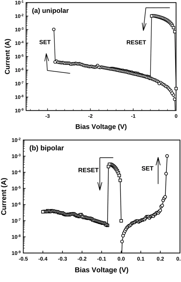
unipolar operation method. As the applied voltage swept to -2.8 V, the device current abruptly increased to the low resistance-state (LRS), which was called the SET process. A compliance current of 1 mA was set to prevent device damage during the SET process. After that, while the applied voltage swept again from 0 to -0.6 V, the device current abruptly decreased to the high resistance-state (HRS), which was called the RESET process. The device current can be reversibly switched between the HRS and the LRS by dc voltages in the same voltage direction, this was called the unipolar operation method. The applied voltage was not swept in the positive direction so as to prevent an electrochemical reaction.
Fig. 1(b) shows that the device current also can be switched by dc voltages in opposite directions, which was called the bipolar operation method. The device current abruptly increased at about 0.22 V and abruptly decreased at about -0.07 V. A compliance current of 1 mA was also set to prevent damage to the device during the SET process. The operation voltages of the bipolar operation method were much smaller than those of the unipolar operation method, which is likely due to different switching mechanisms. The RESET current of the bipolar operation method was also much smaller than that of the unipolar operation
method. The unipolar resistive switching can be explained by the conducting filament model with a thermochemical reaction [8]. The conducting filaments were formed by aligning defects in an electric field during the SET process. The conducting filaments were ruptured by Joule heating during the RESET process. On the other hand, the resistive switching by the bipolar operation method can be explained by the conducting filament model with an electrochemical reaction [7]. While applying a positive voltage on the top electrode, the Cu
atoms near the top electrode dissolved into the SiO2 layer. The Cu ions then migrated through
the SiO2 layer in an electric field and deposited on the Pt bottom electrode. While the Cu
filament grew to reach the top electrode, the conducting filament formed and then the device current switched to the LRS. While applying a negative voltage on the top electrode, the part
of the conducting filament near the top electrode dissolved into the SiO2 layer. As a result, the
conducting filament ruptured and thus the device current switched to the HRS.
As shown in Fig. 2, the difference of the SET process between the unipolar and the bipolar operation methods was analyzed by the current sweeping mode (I-mode). The relation between the resistance and the sweeping current was calculated from the current-voltage (I-V) characteristics. For the unipolar operation method, the device resistance remained constant
while the sweeping current was smaller than 2x10⁻⁵ A. When the sweeping current reached
and exceeded 2x10⁻⁵ A, the device resistance abruptly decreased and then remained almost the
same at about 100 ohm, which indicated the conducting filaments were abruptly and wholly formed. For the bipolar operation method, the device resistance remained constant while the
sweeping current was smaller than 1x10⁻⁵ A. While the sweeping current was larger than
1x10⁻⁵ A, the device resistance decreased gradually as the sweeping current increased, which
indicated that the conducting filament grew in a gradual, continuous fashion. The large RESET current is an issue for RRAM applications. Therefore, many methods have been proposed to reduce the RESET current [9, 10], however, these works have not provided clear avenues of development. Fig. 3 shows the plots of RESET current versus compliance current
using the voltage sweeping mode (V-mode) for the unipolar and the bipolar operation methods. The RESET current increased with an increase of the compliance current. The formation of the conducting filaments was controlled by the compliance current. Therefore, a larger RESET current was needed to rupture more conducting filaments formed under increased compliance current. For the unipolar operation method, the RESET current was larger than the compliance current. On the other hand, for the bipolar operation method, the RESET current was smaller than the compliance current. Therefore, the RESET current of the bipolar operation method was smaller than that of the unipolar operation method, which is likely due to the different rupturing mechanisms of conducting filaments.
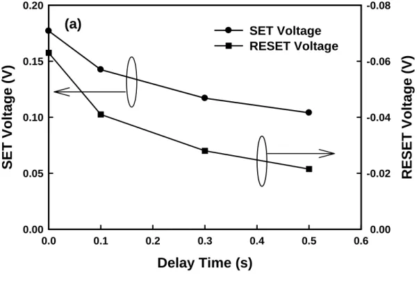
Fig. 4 shows the influences of delay time on the switching voltages and currents using the bipolar operation method. The SET voltage and RESET voltage decreased with an increase of delay time, as shown in Fig. 4(a). Fig. 4(b) also shows the SET current and RESET current decreased with an increase of delay time. In general, the device with one oxidizable electrode and one inert electrode exhibits behaviors consistent with an electrochemical reaction. While a positive voltage was applied to the top electrode, the Cu
ions migrated through the SiO2 film and then electrodeposited on the bottom electrode to form
the Cu conducting filament. While a negative voltage was applied on the top electrode, the Cu filament near the top electrode would dissolve and rupture as a result. With a slow sweeping
speed, Cu ions had more time to migrate through the SiO2 layer to dissolve and electrodeposit
Cu ions. Therefore, smaller switching voltages and current were needed to drive Cu ions to form and rupture the conducting filament. Therefore, the bipolar resistive switching behavior should be charge-controlled. For the unipolar operation method, the switching voltages and currents were independent of the delay time of I-V measurements (not shown). Since the filament rupture is based on a thermochemical reaction, the unipolar switching behavior should be power-controlled [11]. Therefore, the switching mechanisms of the unipolar and bipolar operation methods were not the same. The switching mechanism was not only
influenced by the device structure, but also the operation method. Therefore, the switching mechanism can not be directly determined based solely upon the device structure. The investigation technique outlined in this study provides a method to distinguish between these switching mechanisms.
4. Conclusions
A Cu/SiO2/Pt structure was fabricated to investigate the resistive switching behaviors.
The device resistance was switched by both unipolar and bipolar operations. The unipolar resistive switching took place through a thermochemical reaction. On the other hand, the bipolar resistive switching was through an electrochemical reaction. Due to the different switching mechanisms, the resistive switching behaviors via the two operation methods were quite different. The SET processes of the two operation methods were also investigated by I-mode. In unipolar switching, the conducting filaments were abruptly and wholly formed. In bipolar switching, the conducting filament formed gradually with an increase of the sweeping current. Regarding the RESET process, the relation between RESET current and compliance current of the two operation methods was investigated. The RESET current increased with an increase of compliance current. The RESET current of the bipolar operation method was found to be much smaller than that of the unipolar operation method. A delay time of the V-mode was also adopted in order to investigate the time dependence of resistive switching. For the bipolar operation method, the magnitudes of the switching parameters decreased with an increase of delay time. On the other hand, the switching parameters of the unipolar operation method were independent of delay time. The resistive switching behaviors based upon thermochemical and electrochemical reactions were systematically investigated by unipolar and bipolar operation methods.
Acknowledgements
The authors thank the National Science Council of R.O.C. for financial supports under project No. NSC 98-2221-E-151-058 and the facility support from National Nano Device Laboratories.
References
[1] D. C. Worledge, D. W. Abraham, Appl. Phys. Lett. 82 (2003) 4522.
[2] X. S. Miao, L. P. Shi, H. K. Lee, J. M. Li, R. Zhao, P. K. Tan, K. G. Lim, H. X. Yang, T. C. Chong, Jpn. J. Appl. Phys. 45 (2006) 3955.
[3] A. Beck, J. G. Bednorz, Ch. Gerber, C. Rossel, D. Widmer, Appl. Phys. Lett. 77 (2000) 139.
[4] C. Y. Liu, P. H. Wu, A. Wang, W. Y. Jang, J. C. Young, K. Y. Chiu, T. Y Tseng, IEEE Electron Device Lett. 26 (2005) 351.
[5] C. Y. Liu, X. J. Lin, H. Y. Wang, C. H. Lai, Jpn. J. Appl. Phys. 49 (2010) 056507.
[6] H. B. Lv, M. Yin, Y. L. Song, X. F. Fu, L. Tang, P. Zhou, C. H. Zhao, T. A. Tang, B. A. Chen, Y. Y. Lin, IEEE Electron Device Lett. 29 (2008) 47.
[7] C. Schindler, S. C. P. Thermadam, R. Waser, M. N. Kozicki, IEEE Trans. Electron Devices 54 (2007) 2762.
[8] D. S. Jeong, B. J. Choi, C. S. Hwang, J. Appl. Phys. 100 (2006) 113724.
[9] S. E. Ahn, M. J. Lee, Y. Park, B. S. Kang, C. B. Lee, K. H. Kim, S. Seo, D. S. Suh, D. C. Kim, J. Hur, W. Xianyu, G. Stefanovich, H. Yin, I. K. Yoo, J. H. Lee, J. B. Park, I. G. Baek, B. H. Park, Adv. Mater., 20 (2008) 924.
[10] K. Kinoshita, K. Tsunoda, Y. Sato, H. Noshiro, S. Yagaki, M. Aoki, Y. Sugiyama Appl. Phys. Lett. 93 (2008) 033506.
(2002) 262907.
Figure Captions
Fig. 1 Plots of current versus bias voltage of the Cu/SiO2/Pt device using (a) the unipolar
operation method and (b) the bipolar operation method. The SET and RESET labels indicate that the device has switched to a low or high resistance-state respectively.
Fig. 2 Plots of resistance versus sweeping current of the Cu/SiO2/Pt device using the
unipolar and the bipolar operation methods.
Fig. 3 Plots of RESET current versus compliance current using the voltage sweeping mode for the unipolar and the bipolar operation methods.
Fig. 4 (a) Influences of delay time of current-voltage measurements on SET voltage and RESET voltage, and (b) influences of delay time of current-voltage measurements on SET current and RESET current.
Bias Voltage (V)
-3 -2 -1 0Curren
t (A)
10-9 10-8 10-7 10-6 10-5 10-4 10-3 10-2 10-1 RESET SET(a) unipolar
Bias Voltage (V)
-0.5 -0.4 -0.3 -0.2 -0.1 0.0 0.1 0.2 0.3Current (A)
10-9 10-8 10-7 10-6 10-5 10-4 10-3 10-2(b) bipolar
SET
RESET
Sweeping Current (A)
10-8 10-7 10-6 10-5 10-4 10-3 10-2Resistance (Ohm)
101 102 103 104 105 106unipolar
bipolar
Fig. 2 Liu et al.
Compliance Current (A)
10-4 10-3 10-2 10-1
RESET Curren
t (A)
10-4 10-3 10-2 10-1unipolar
bipolar
I
RESET= I
ComplianceDelay Time (s)
0.0 0.1 0.2 0.3 0.4 0.5 0.6SET Voltage (V)
0.00 0.05 0.10 0.15 0.20RESET Voltage (V)
-0.08 -0.06 -0.04 -0.02 0.00 SET Voltage RESET Voltage(a)
Delay Time (s)
0.0 0.1 0.2 0.3 0.4 0.5 0.6SET Current (A)
10-11
10-10
10-9
RESET Current (A)
10-4
10-3
SET Current RESET Current
(b)
98 年度專題研究計畫研究成果彙整表
計畫主持人:劉志益 計畫編號: 98-2221-E-151-058-計畫名稱:後段製程材料於電阻式記憶體元件與材料之研究(I) 量化 成果項目 實際已達成 數(被接受 或已發表) 預期總達成 數(含實際已 達成數) 本計畫實 際貢獻百 分比 單位 備 註 ( 質 化 說 明:如 數 個 計 畫 共 同 成 果、成 果 列 為 該 期 刊 之 封 面 故 事 ... 等) 期刊論文 0 0 100% 研究報告/技術報告 0 0 100% 研討會論文 0 0 100% 篇 論文著作 專書 0 0 100% 申請中件數 0 0 100% 專利 已獲得件數 0 0 100% 件 件數 0 0 100% 件 技術移轉 權利金 0 0 100% 千元 碩士生 0 0 100% 博士生 0 0 100% 博士後研究員 0 0 100% 國內 參與計畫人力 (本國籍) 專任助理 1 1 100% 人次 期刊論文 3 3 100% 研究報告/技術報告 0 0 100% 研討會論文 3 3 100% 篇 論文著作 專書 0 0 100% 章/本 申請中件數 0 0 100% 專利 已獲得件數 0 0 100% 件 件數 0 0 100% 件 技術移轉 權利金 0 0 100% 千元 碩士生 0 0 100% 博士生 0 0 100% 博士後研究員 0 0 100% 國外 參與計畫人力 (外國籍) 專任助理 0 0 100% 人次其他成果