Abstract--This paper describes a design of time-to-digital converter (TDC) utilizing a two-level conversion scheme. The first level is accomplished by a multi-phase sampling technique with the aid of delay-locked loop (DLL). Then the input signal and its adjacent sampling clock are manipulated and sent into a vernier delay line (VDL) sampling circuit. The proposed TDC can provide precise resolution with less hardware comparing to one level VDL sampling circuit possessing the same dynamic range. A new architecture of dual DLL circuit is also introduced to stabilize delay control against process and ambient variation. The test chip is designed and fabricated in 0.35µm digital process. With an input reference clock at 160MHz, the TDC achieves 24ps resolution. The DNL is less than ±0.55LSB and INL within +1LSB~-1.5LSB.
I. INTRODUCTION
IME-to-Digital Converter (TDC) has been widely used in many applications such as particle life time detection in high energy physics[1-3], equivalent-time sampling in oscilloscope[4], and laser range finder[5], etc. Traditional analog approaches such as dual slope and time-to-amplitude methods are slow and vulnerable to system noise. New digital approaches using DLL have been widely adopted because DLL can provide accurate multi-phase sampling clocks and has the merit of low power. Due to the limitation of intrinsic delay of the delay buffer in DLL, several techniques based on the gate delay difference can improve the resolution up to sub-gate delay. The DLL array[2], multi-level[5] and vernier delay line (VDL)[3] methods have been presented. The VDL method provides excellent fine resolution but suffers from large chip area if wide dynamic range is required. Here we will present a two-level conversion scheme combining the multi-phase sampling and VDL sampling methods to alleviate the burden of the large number of delay stages in VDL method for a fixed dynamic range.
Manuscript received Oct 29, 2003.
Chorng-Sii Hwang and Hen-Wai Tsao are with the Department of Electrical Engineering and Graduate Institute of Electronics Engineering, National Taiwan University, Taipei, Taiwan, 10617 ROC (telephone: +886-2-23635251 ext 213, e-mail: tsaohw@cc.ee.ntu.edu.tw).
Poki Chen is with the Department of Electronic Engineering, National Taiwan University of Science and Technology , Taipei, Taiwan, 10650 ROC (telephone: +886-2-27376400, e-mail: poki@et.ntust.edu.tw).
II. PRINCIPLE OF OPERATION
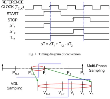
Many TDC systems accept two asynchronous START/STOP input signals and resolve their time difference. The timing diagram is depicted in Fig.1. The key design issue is the fine measurement of the time intervals (∆T1, ∆T2) between the rising edges of START/STOP pulses and their succeeding reference clocks (TCLK). Thus, the dynamic range of the fine time digitization can be limited to one reference clock cycle only. The overall dynamic range can be further extended by a digital counter (T12).
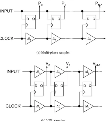
The fine time conversion process in the proposed TDC is divided into two levels as shown in Fig.2. Firstly, the rising edge of the input signal is digitized by N-stage equal-phase sampling clocks as shown in Fig.3(a). Then, the input signal and its adjacent sampling clock are fed into an M-stage VDL sampler illustrated in Fig.3(b). The resolution in the first level should be an integer multiple of the one in the second level. Thus, the resolution of the fine time conversion becomes TCLK/(M*N). The dynamic range of VDL used in the second level can be restricted to only a fraction of the whole reference clock cycle (=TCLK/N). REFERENCE CLOCK (TCLK) START STOP ∆T1 ∆T2 T12 ∆T = ∆T1 + T12 - ∆T2
Fig. 1. Timing diagram of conversion
VDL Sampling Multi-Phase Sampling P0 P1 Pi Pi+1 PN-1 Vj V1 V0 Vj+1 VM-1
Fig. 2. Two-level conversion scheme
A High-Precision Time-To-Digital Converter
Using A Two-Level Conversion Scheme
Chorng-Sii Hwang, Student Member, Poki Chen, Hen-Wai Tsao, Member, IEEE
T
D Q D Q ∆tf D Q CLOCK INPUT ∆tf ∆tf P0 P1 PN-1
(a) Multi-phase sampler
D Q ∆tf CLOCK' INPUT' V0 D Q ∆tf V1 ∆ts ∆ts D Q ∆tf VM-1 ∆ts (b) VDL sampler
Fig. 3. Two architectures of time samplers
III. CIRCUITDESCRIPTION
The architecture of the proposed TDC is shown in Fig.4. The difficulty in designing the two-level conversion scheme results from selecting the sampling clock adjacent to the input signal. Decision must be made before sending sampling clock into the second level circuitry. The easiest way is to employ the sampling results of the DFF’s. However, the DFF’s used in the multi-phase sampler will suffer from the setup time violation. If the input signal and the sampling clock are very close, the resolving time of DFF’s will become longer. The solution to this problem is to introduce an extra stage of DFF’s after the sampler outputs as shown in Fig.5. The first level sampler output is re-aligned to the other sampling output by waiting a half clock cycle. The re-aligned outputs can then be sent into a dynamic NOR gate to extract the adjacent sampling clock information. At the same time, we must also add a delay path for the input signal to compensate the increased delay in the sampling clock path. The delayed input signal and its adjacent sampling clock are sent into the VDL sampler.
In order to obtain the delay control of the multi-phase sampler and the vernier sampler, a dual DLL architecture is proposed as shown in Fig.6. The “fast” DLL contains N-stage delay buffers and regulates their delay to be ∆tf (=TCLK/N). Then we choose the output of the (N+1)th delay buffer from the “fast” DLL to match with the output of the Nth delay buffer in the “slow” DLL. It forces the delay of the delay buffers in the “slow” DLL to be ∆ts (=[TCLK/N]*[N+1]/N=TCLK*[N+1]/N2).
Then the resolution ∆tr in VDL can be obtained by the delay difference of the two gates :
∆tr = ∆ts –∆tf = [TCLK*(N+1)/N2] - (TCLK/N) = TCLK/N2 Thus, the delay stage number (M) in VDL sampler is the same as the number of the multi-phase sampler. The main advantage of such a dual DLL is that it needs only a single reference clock instead of two phase-delayed reference clocks proposed in the previous work[3].
Multi-Phase Sampler Vernier-Delay Line Sampler N INPUT CLOCK N Dual DLL TCLK*[N+1]/N2 TCLK/N VBNF VBNS VBNS VBNF VBNF INPUT' CLOCK'
Fig. 4. Chip architecture
D Q P P0 D Q P P1 N 2 N 2+ 1 P'0 P'1 D Q P -1 PN-1 N 2 P'N-1
Fig. 5. Re-aligning circuit in the first level
1 2 3 1 2 3 N N N+1 PD + CP PD + CP REFERENCE CLOCK VBNF Fast DLL Slow DLL VBNS Fig. 6. Dual DLL
IV. IMPLEMENTATION AND MEASUREMENT
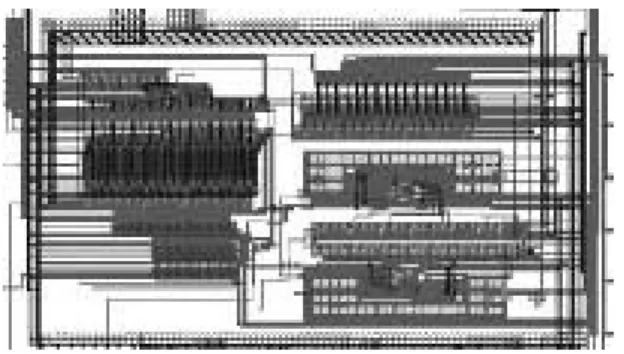
The test chip of the proposed TDC has been designed and fabricated in TSMC 0.35µm SPQM Silicide process. The TDC uses 16 stages in both levels and provides 256 LSB’s in one reference clock cycle. The layout diagram is shown in Fig.7. The core area of the two-level TDC is 1,000 x 600 um2. We use HP 81200 Data/Pulse Generator with 2ps delay step to characterize the test chip. The TDC is running at a clock rate of 160MHz corresponding to one LSB of 24ps (=6.25ns/162). The DNL is less than ±0.55LSB and INL within +1LSB~-1.5LSB as shown in Fig.8. The overall performance is summarized in Table.1 The worst case of INL and DNL are mainly caused by the mismatch of layout paths in the multi-phase sampler and the crosstalk of input signals.
Fig. 7. Layout diagram of the proposed TDC -1.8 -1.3 -0.8 -0.3 0.2 0.7 1.2 0 50 100 150 200 250 DNL INL
Fig. 8. DNL and INL
Operating Voltage 3.0V~3.6V Temperature 0o~+60o Reference Clock 160MHz TCLK-1 Delay Stage 16 N Bin Size 256 N2 LSB 24ps TCLK/N2 Power < 50mW
Table 1. Performance Summary
V. CONCLUSION
In this paper, a high-precision TDC using a two-level conversion scheme has been proposed and fabricated. By employing the technique of multi-phase sampling, the stage number of the second-level VDL sampler can be further reduced. A dual DLL providing delay regulation with single reference clock input is also presented. The test chip achieves 24ps resolution with DNL less than ±0.55LSB and INL within +1LSB~-1.5LSB.
VI. ACKNOWLEDGMENT
The authors would like to thank the Chip Implementation Center (CIC) of the National Science Council, Taiwan, R.O.C., for fabricating the chips and the Instrument R&D Division in Center for Measurement Standards (CMS) of Industrial Technology Research Institute (ITRI), Taipei, Taiwan, R.O.C. for helping in characterizing the chips.
VII. REFERENCES
[1] D. Santos, S. Dow, J. Flasck and M. Levi, “A CMOS delay locked loop and sub-nanosecond time-to-digital converter chip”, IEEE Trans. on
Nuclear Science, vol. 43, pp. 1717-1719, Jun. 1996.
[2] J. Christiansen, “An integrated high resolution CMOS timing generator based on an array of delay locked loops” IEEE J. Solid-State Circuits, vol. 31, pp. 952-957, Jul. 1996.
[3] P. Dudek, S. Szczepanski and J. V. Hatfield, “A high resolution CMOS time-to-digital converter utilizing a vernier delay line” IEEE J.
Solid-State Circuits, vol. 35, pp. 240-247, Feb. 2000.
[4] K. Park and J. Park, “20ps resolution time-to-digital converter for digital storage oscilloscopes”, IEEE Nuclear Science Symposium, vol.2, pp.876 -881, 1998.
[5] A. Mantyniemi, T. Rahkonen and J. Kostamovaara, “An integrated 9-channel time digitizer with 30ps resolution”, IEEE International
Solid-State Circuits Conference, pp.266-267 Feb. 2002.