698 IEEE TRANSACTIONS ON ELECTRON DEVICES, VOL 41, NO. 5, MAY 1994
The Effects of Fluorine Passivation
on Polvsilicon Thin-Film Transistors
JHorng Nan Chern, Chung
Abstract-The fluorine implantation on polysilicon was found to improve the characteristics of polysilicon thin-film transis- tors (TFT's). The fluorine passivates the trap states within the polysilicon channel. As compared with the HZ -plasma passivation, the fluorine implantation passivates more uniformly both the band tail-states and midgap deep-state, while the HZ -plasma treatment is more effective to passivate deep states than tail states. A fluorine-implanted device can be further improved its performance if an Hz-plasma treatment is applied. In contrast to the H2-plasma passivation, the fluorine passivation improves the device hot-carrier immunity. Combining the fluorine passivation and H2-plasma passivation, a high performance TFT with a high hot-carrier immunity can be obtained.
I. INTRODUCTION
N order to obtain desirable characteristics of polysilicon
I
TFT's, many techniques had been employed to improve the device performance by reducing the trap-state density or increasing the grain size of the polysilicon. Hydrogenation is an effective method to improve the TFT performance [1]-[3]. Also, the 02-plasma treatment [4], [5] or the H 2 / 0 2 - plasma treatment [5] have been found to improve the TIT performance. However, either the Ha-plasma treatment or the 02-plasma treatment, will loss their the passivation effect when the passivated samples are subjected to high temperature(>
500" C) annealing. Also, it had been found that the H2- plasma applied on a MOS capacitor creates positive charges in the oxide, hence, causing an undesirable flatband voltage shift of the device [6], [7]. Furthermore, it was reported that [8], [9] TFT's, after the H2-plasma passivation, suffer a low hot- carrier endurance. For the H2-plasma passivation, it is easy to passivate dangling bonds in grain boundaries to reduce the midgap deep states, while it needs a very long hydrogenation- time(>
4 hr) to passivate the strain-bond-related tail states [3]. However, it has been reported that the fluorine can break strained bonds, likely the strained Si-0-Si bonds and the Si- Si bonds to cause local strain relaxation [12]-[14] and to reduce the interface states [ 131. Also, it was reported that [ 121 fluorine may break a weak Si-H bond or a weak Si-OH bond to form a strong Si-F bond in its place at the Si/SiOz interface. With the fluorine implantation in the Si/SiO2 interface, an MOS has a better irradiation and hot-carrier resistance [ 121. Recently, H. Kitajima et al. had found thatF+
implantation is Manuscript received August 24, 1993; revised November 15, 1993. The review of this paper was arranged by Associate Editor J. R. Pfiester. This work was supported by the National Science Council of the R.O.C. under Contract Number NSC-82-0404-E009- 190.The authors are with the Department of Electronics Engineering and Institute of Electronics, National Chiao Tung University, Hsinchu, Taiwan, R.O.C.
IEEE Log Number 9215968.
Len Lee. and Tan Fu Lei
effective to increase the ON-current of polysilicon TFT's by improving their subthreshold swings [ 151. However, they did not study the effects of flourine on the defect passivation and the hot-carrier resistance of TFT's.
This paper studies the fluorine implantation into the polysil- icon TFT to improve its performance. It is found that the fluorine implantation does not only improve the initial charac- teristics of a TFT but also improves the hot-carrier immunity of the device. It can be combined with the use of the Ha- plasma passivation to produce a high performance and a high hot-carrier TFT. It is also found that fluorine passivation is more uniformly to reduce the trap states in the band tail and those in the midgap, while the H2-plasma passivation is more effective to reduce the trap states in the midgap than in the band tail.
11. DEVICE PREPARATION
The polysilicon TFT's studied in this work were prepared as follows: An amorphous silicon film of a thickness of approximately 600w was deposited at 500OC by a low-pressure chemical vapor deposition (LPCVD) system on thermally oxidized silicon wafers. The wafers were then annealed at 600°C for 20 hours to transform the amorphous film to polysilicon. After defining the active islands, a 200w pad oxide was grown at 850°C. Fluorine ions with doses from 2 x cmP2 to 2 x 10" cmP2 at 25 keV were implanted through the pad oxide to the polysilicon film. After annealing at 850OC for 60 min in an Nzgas, the pad oxide was removed and then a 300w gate oxide was grown in dry 0 2 at 850°C. Another
3000w polysilicon film was then deposited at 625°C by the LPCVD system to be the gate electrode. After defining the gate pattern, a self-aligned phosphorus or BF; implantation of a dose of 2 x 10¹⁵ cniP2 was performed to form the source, drain and gate electrodes for N-channel and P-channel devices respectively. The dopants were activated at 850°C for 35 min in an NZ atmosphere. Some of the samples were subjected to the H2/N2 plasma treatment in a commercial plasma-enhanced chemical vapor deposition (PECVD) system at 300°C for 1 hour. All devices were covered with a 5000A PECVD Si02 for passivation. Contact holes were opened, and A1 was deposited and then patterned.
111. MEASUREMENT RESULTS AND DISCUSSIONS
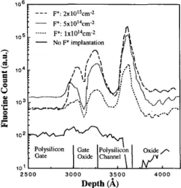
A . Effects of Fluorine on the Characteristics of TFT's Fig. 1 shows the SIMS profiles of fluorine after the dopant- activation annealing for the devices implanted with different
fluorine doses of 1 x 10¹⁴ cmP2
and without a fluorine implantation respectively. It is seen that 5 x 10l4 crnP2, 2 x
CHERN ef al.: THE EFFECTS OF FLOURINE PASSIVATION
1 0 1
699
:
Polysilicon Gate Polysilicon. Gate Oxide Channel
,iI
.PT
10.’ I I I I 1 I I F+: 2 ~ 1 0 ’ ~ c m - ~ F+: 5 ~ 1 0 ’ ~ c m - * F+: l ~ l O ’ ~ c m - * No F+ implantation
!.
fi /?II
0 5 10 15 20 25 Gate Voltage Vg(V)Fig. 2. Ig-\b Characteristics for the gate oxides implanted with 2 x 10I3 F/cm2.2 x 10ls F/cm2 and without fluorine implantation respectively. The inserted table shows the breakdown voltages of these three devices. The device area was 7 X 10⁻⁴c111-2 .
for all the fluorine-implanted devices, the fluorine tail extended deep into the channel while most fluorine piled up at the Si/SiOz interface. There was also some fluorine existing in the gate oxide. Fig. 2 shows the Ig-Vg characteristics, which were measured by grounding the source and drain electrodes but applying a
V,
to the gate electrode, for devices implanted with 2 x 10¹³ F/ cm2 , 2 x F/ cm2 and without F implantation respectively. The insert shows a table which compiles the breakdown voltages for the devices of Fig. 2. It is seen that the gate-oxide breakdown voltage was increased for the devices implanted with fluorine, and the more the fluorine dose, the higher the gate oxide breakdown voltage. This is different from the previous reports on the single-crystalline Si/SiOp where fluorine did not affect or even degrade the oxide breakdown strength [16], [17]. From C-V measurement, we did not find the thickening of the gate oxide after the flourine incorporation [16], [17]. The increase of the breakdown voltage may be due to the formation of strong Si-F bonds and the stress relaxation in the gate oxide network [14] and in the polysilicon.Fig. 3(a) and (b) shows the Id-Vg characteristics of the TFT’s implanted with 2 x F/cm2, 2 x 10¹⁵ F/cm2 and
1 o - ~ h 4 l o 5 * I O S
1
107:
I O 8 1 0 9 P I 1 o-’O 10.” I I I I I I I - 1 0 - 5 0 5 1 0 15 2 0 Gate Voltage (V) (a) 1 0 . ~ I I I I 1 P CI +, -z
10-7 - 3 ... I O ” I I I 1 1 I I -20 - 1 5 - 1 0 - 5 0 5 1 0 Gate Voltage (V) (b)Fig. 3. The Id-\; characteristics at \ > = 5V of (a) N-channel, and (b) P-channel polysilicon TIT’S implanted with 2 x 10’” 2 x 10¹⁵ fluorine/cm* and without fluorine implantation respectively.
without F implantation for N-channel and P-channel devices respectively. It is seen that the subthreshold and the ON- state characteristics of the implanted devices were much improved, and the higher the dose of fluorine was, the greater improvement was. However, the OFF-state leakage currents were nearly unchanged. These results are consistent with the previous report by H. Kitajima et al. [15]. The temperature dependence of the drain current for the devices of Fig. 3(a) and (b) was also measured in the temperature range from 25°C to 150°C. Using the linear fitting of the l n ( 1 d ) versus the 1 k . T plot, where
k
is the Boltzmann constant and T is the temperature, the activation energy E, of the drain current at different gate biases is deduced. Figs. 4(a) and (b) show the activation energies of the drain currents as a function of the gate voltage at Vd = 0.1V for the devices of Fig. 3(a) and (b), respectively. We can clearly see that the fluorine implantation reduced the activation energy. The value ofthe activation energy reflects the carrier transport barrier of the grain boundary within the polysilicon channel. This implies that the trap states in the channel are passivated by flourine, and hence the grain-boundary barrier potential are reduced. We believe that there are two mechanisms to cause the improvement on the characteristics of flourine-implanted devices. One is that flourine breaks strained bonds to form Si- F bonds. Another is that flourine passivates dangling bonds. The first mechanism causes the decrease of band tail states and the second mechanism causes the decrease of midgap deep states. These two mechanisms do not only occur in polysilicon channel but also occur at the Si/SiOz interface to passivate the
700
$
,oo 120*
2
8o%
v1 & 60IEEE TRANSACTIONS ON ELECTRON DEVICES, VOL 41, NO. 5, MAY 1994
w/L= 4opm/8w
1
Stressed at Vd= 1OV and Vg= 1OV.
-c NoPimplanIation -bF+ : 2x10"-
-t F+ :2~1015cm-Z 0.7 I I I I I I 0 . 6c
mm 0 . 5kd
0 . 4t
1
0.3.s
ca 0.2 .t c9
0.1 -.. 0 I I I I - 1 0 - 5 0 5 1 0 1 5 Gate Voltage (V) (a) - -'
- - - 0.7 I I I I I 3,0E
2.5 v h *8
1.5a
0.5 0.0 1Stressed at Vd= 1OV and Vg= 1OV
-
No F implantation-
-
F+ :2x1013cm.z --t F+ : Z X ~ O ' ~ cm-2:
. ....A
.
4 No F' Implantation - 4 - F+: 2x10'~ cm-2 - - D - F + : M o I ~ cm-2 P-channel .u.. 0 I I I I1
- 1 5 - 1 0 - 5 0 5 1 0 Gate Voltage (V) (b) Fig. 4.and ( b ) P-channel TFT's implanted with 2 x without fluorine implantation, respectively.
The activation energies of the drain currents for (a) N-channel TFT's,
2 x IOl5 fluorine/cmz and
interface states. From the trap state measurement, which is discussed in Section B, Fig. 7, it is clearly seen that both the tail states and deep states in polysilicon channel we reduced for the flourine-implanted devices.
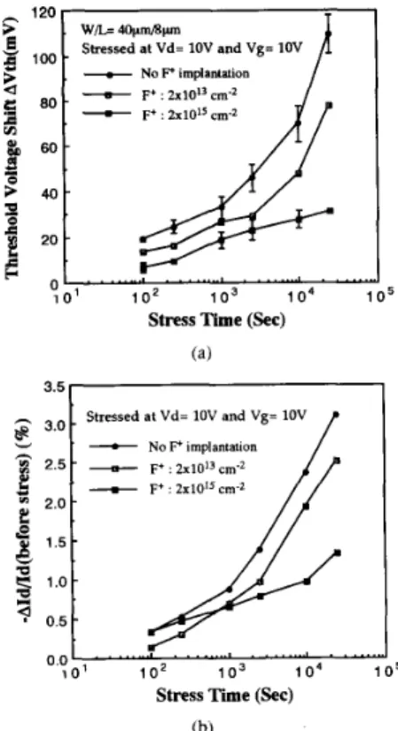
The hot-carrier reliability of the fluorine-implanted devices was also investigated. Fig. 5(a) and (b) show the threshold- voltage shift and the drain-current reduction for the devices of Fig. 3(a), respectively after they were stressed at
Vd
= 1OV andV,
= 1OV for different times. It is found that the hot-carrier-induced degradation was suppressed for the fluorine-implanted devices and the more the implanted dose, the more suppression. For a polysilicon TIT, the degradation induced by hot-carrier stress is thought to be due to the generation of Si/SiO2 interface states and/or the breaking of Si-H bonds at grain boundaries [8], [9]. It is possible that weak Si-H bonds in polysilicon channel and at the Si/SiO2 interface had been replaced by stronger Si-F bonds. This mechanism can explain the improved hot-carrier immunity for the flourine-implanted devices, but does not further passivate trap states.B . Comparison of Fluorine Passivation
and Hydrogen Passivation
As mentioned previously, hydrogen passivates more easily dangling bonds but more difficulty strain bonds [3]. The strain bonds which are associated with dislocations and microtwins in the polysilicon channel are the main source of tail-states in the forbidden band [3], [ 1 11 and they affect the leakage current and the mobility of the TFT's [3], [lo]. It had been reported
I
1 o 5 Stress Time (Sec)(b)
Fig. 5. (a) The threshold voltage shift, and (b) the drain current reduction
(measured at I,> = 5V and I\ = 1 5 V ) for the fluorine-implanted and unimplanted devices after they were stressed at Ill = 1OV and I,\ = 1OV for different times. The device dimension was W/L = 40jtm/8pm.
that fluorine can break strained Si-Si bonds or strained Si-0- Si bonds to form Si-F bonds and cause local strain relaxation. Hence, it is worthwhile to investigate the difference between the fluorine passivation and the hydrogen passivation on polysilicon defects. N-channel and P-channel TFT's were then applied with a fluorine implantation, an Hz-plasma passivation, and a fluorine implantation
+
an H2-plasma passivation, and their characteristics were measured. Tables I (a) and (b) compile the threshold voltage, the subthreshold swing, the minimum drain current and the mobility for the TFT's without any passivation, with the 2 x 10¹⁵ F/cmz implantation, with the Hz-plasma passivation, and with the 2 x 10¹⁵F/cm2 implantation+
the H;?-plasma passivation, respectively. The threshold voltageVth
is defined from the intercept on the voltage axis of the straight line in the drain currentId
versus the gate voltageV,
plot with the device operated in the linear region. The field-effect mobility p is also derived from theId-vg
plot by operating the device in the linear region. The leakage current I m i n is the minimum value of the drain current at V, = 5V for N-channel devices and v d = 5V for P-channel devices. It is seen that the fluorine passivation was more effective to improve the mobility and the hydrogen passivation was more effective to improve the threshold voltage and the subthreshold swing, and combining the fluorine and hydrogen passivations, we can obtain the best device performance. Fig. 6(a) and (b) show the threshold voltage and the subthreshold swing as a function of fluorine dosage for both the N-channelC H E W et al.: THE EFFECTS OF FLOURINE PASSIVATION h 0
#
a2
0.30s
*
0.25s
.I1
g
0.20 a*
70 I-
--
TABLE ITHE V ALUES OF THE DEVICE PARAMETERS OF THE POLYSILICON TFT's
WITHOUT PASSIVATION. WITH 2 x 10'' F / c ~ n " I MPLANTATION, WITH
HYDROGENATION, AND WITH 2 x F/crn' IMPLANTATION
+
HYDROGENATIONFOR (a) N-CHANNEL DEVICES AND (b) P-CHANNEL DEVICES, RESPECTIVELY
(a) N-channel TFT
Parameters
vt
h S Imm 11Condition (V) (Vldec) (DA) (cm2 N . sl
No Passivation 10.3 1.16 24.5 3.3 F: 2 x 1 0 ' ~ c m - * 8.5 0.74 36.6 11.0 Hydrogenation 3.0 0.33 22.0 12.0 F: 2 x 1015cm-2 0.5 0.17 17.4 20.2
+
hvdrogenation (b) P-channel TFT No Passivation -9.8 0.98 -54.0 6.9 F: 2 x 10'~cm-* -6.9 0.80 -68.8 12.1 Hydrogenation -4.0 0.29 -39.0 10.8 F: 2 x 1 0 ' ~ c m - ~ -1.9 0.18 -31.1 14.6+
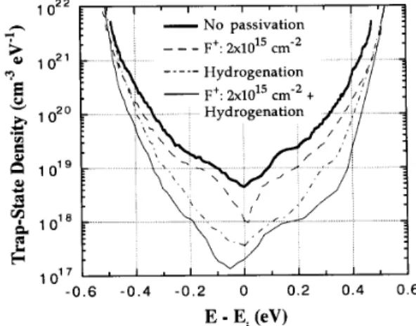
hydrogenationand P-channel devices after hydrogenation respectively. It is seen that the performances of the fluorine-implanted devices were further improved after the hydrogenation and the more the device was fluorine-implanted, the better the device perfor- mance was. We had reported that [18], the H2-plasma passiva- tion effect saturates as the passivation time is above 40 min. In this experiment, the passivation time was 60 min, which was expected to reach the passivation-effect saturation by hydro- gen. Hence, the improvement of these hydrogenated fluorine- implanted devices was believed to be due to the further fluorine passivation effect. This further passivation effect could passivate those defects which were difficult to be passivated by the hydrogen-plasma only. Fig. 7 shows the trap-state density distributions in the forbidden band for the devices of Table I. The trap-state density distributions were calculated by using the field-effect analysis [ 191, [20]. It is seen that the hydrogen passivation was more effective to passivate deep states than tail states, while the fluorine passivated more uniformly both the tail states and deep states. However, for the device subjected to jointly the fluorine-passivation and the hydrogen passivation, the trap state density was the smallest in both the deep level and the tail level than the devices subjected to the fluorine- passivation only or the hydrogen-passivation only.
Fig. 8 shows the threshold voltage shift and the subthreshold swing for the devices with the fluorine passivation and the hydrogen passivation, respectively, after they were stressed at V d = 15
V. V,
= 10V
for lo4 s. It is found that the hydrogen- passivation decreased the hot-carrier endurability of the device, while the fluorine-passivation increased the hot-carrier en- durability, and the fluorine implantation also increased the hot-carrier endurability for the hydrogen-passivated devices. Fig. 9 shows the threshold voltage shift for hydrogenated P- channel devices implanted with different doses of flourine after they were stressed at Vd = -18V. V, = 15V for lo4 s. It is seen that similar improvement on hot-carrier immunity is obtained although the P-channel devices have a smaller60 min Hz-plasma treatment
\.
*
N-Channel.-..
--+- P-Channel'.
1.
"."I,
60 min Hz-plasma treatment
(b)
Fig. 6. The variations of (a) the threshold voltage, and (b) the subthreshold swing of hydrogenated N-channel and P-channel devices as a function of the fluorine dose. The device dimension was I17/L = 1 0 p m / l O ~ t m .
- - -
F+ zX10l5 cm-2-0.6 - 0 . 4 -0.2 0 0.2 0.4 0 6
E
-
E, (eV)
Fig. 7 The trap-state density distnbutiom for the devices of Table I.
hot-carrier-induced degradation than that of the N-channel devices. Fig. 9 also shows that the distribution of -AVth is narrower for the flourine-implanted devices than that for the unimplanted device. From the above results, it is reasonable to suspect that the weak Si-H bonds in polysilicon channel and at
702 IEEE TRANSACTIONS ON ELECTRON DEVICES, VOL 41, NO. 5, MAY 1994
1 4 0 I I I 60 temperature poly-Si n-channel TFT’s for LCD,” IEEE Trans. Eelctron
W L = 20Cun/8pm
Stressed at V,=lSV, V =1OV for lo4 sec
Devices, vol. 36, pp. 351-359, 1989.
[3] I-W. Wu, T-Y. Huang, W. B. Jackson, A. G. Lewis, and A. C. Chiang, “Passivation kinetics of two types of defects in polysilicon TFI by plasma hydrogenation,” IEEE Electron Device Lett., vol. 12, pp. [4] S. Ikeda, S. Hashiba, I. Kuramoto, H. Katoh, S. Ariga, T. Yamanka, T. Hashimoto, N. Hashimoto, and S. Megura, “A polysilicon transistor technology for larger capacitance SRAMS,” in IEDM Tech. Dig.. 1990, (51 H. N. Chem, C. L. Lee, and T. F. Lei, “Hz/Oz plasma on polysilicon
thin film transistor,” IEEE Electron Device Lett., vol. 14, pp. 115-1 17, [6] Y. Chung, C. Y. Chen, D. W. Langer, and Y. S. Park, “The effect of
Sci. Techno/., vol. B1, no. 3, pp. 799-802, 1983.
[7] J. Kassabov, “UV and plasma effects in the Si/SiO2 system,” in 1991
Insulating Films On Semiconductors, W. Eccleston and M. Uren, Eds. 1 20
--
I Hydrogenation h 181-183, 1991. 4 04
g
CA pp. 459463. -a
- 20 4 0 - 2 0-
1993.I I 1 low pressure plasma on Si-Si02 structure and GaAs substrate,” J. Vac.
0 10
F+ Implant Dose (an-’)
N O F + 1014 1 0 ’ ~ 1 0 ’ 8
Implant
Fig. 8. The changes of the threshold voltage and the subthreshold swing of polysilicon T l T s measured at bi = 0.1V as a function of fluorine dose after they were stressed at \ > = 15V and 1; = 1OV for l o 4 s.
100
1
I I II
A A A A A1
0-1 I I I 1 NO F* 1013 1 0 ’ ~ 1 0 ’ ~ 1 O t 6 Implant F+ implant Dose (cm-’)Fig. 9. The changes of the threshold voltage of hydrogenated P-channel polysilicon TFT’s measured at V, = 0.1V as a function of flourine dose after they were stressed at V,, = -18V and \> = -15 for 104s.
the SiOz/Si interface, which are thought to be the main source for the hot-carrier-induced degradation, had been replaced by stronger Si-F bonds as described in Section 111-A.
IV. CONCLUSION
This paper reports that the fluorine implantation on the polysilicon improves the characteristics of a polysilicon TFT. It has been shown that the improvement is due to the in-
Bristol: Adam Hilger, pp. 3 3 4 2 .
[8] S. Banerjee, R. Sundaresan, H. Shichijo, and S. Malhi, “Hot-camer degradation of n-channel polysilicon MOSFET’s,” IEEE Trans. EIectron
Devices, vol. 35, pp. 152-157, 1988.
[9] M. Hack, A. G. Lewis, and I-W. Wu, “Physical models for degrada- tion effects in polysilicon thin-film transistors,” IEEE Trans. Electron
Devices, vol. 40, pp. 890-897, 1993.
[IO] K. Ono, T. Aoyama, N. Konishi, and K. Miyata, “Analysis of current- voltage characteristics of low-temperature-processed polysilicon thin- film transistors,” IEEE Trans. Electron Devices, vol. 39, pp. 890-897, 1992.
[ l 11 P. Migliorato and D. B. Meakin, “Material properties and characteristics of polysilicon transistors for large area electronics,” Appl. Sur. Sci., vol. 30, pp. 353-371, 1987.
(121 T. P. Ma, “Effects of fluorine on MOS properties,” Mat. Res. Soc. Symp. Proc., vol. 262, pp. 741-139, 1992.
[I31 D. N. Kouvatsos, F. A. Stevie, and R. J. Jaccodine, “Interface state density reduction and effect of oxidation temperature on fluorine in- corporation and profiling for fluorinated metal oxide semiconductor capacitors,” J. Electrochem. Soc., vol. 140, no. 4, pp. 1160-1 164, 1993. [14] D. Kouvatsos, J. G. Huang, and R. J. Jaccodine, “Fluorine-enhanced
oxidation of Silicon: effects of fluorine on oxide stress and growth kinetics,” J. Electrochem. Soc., vol. 138, no. 6, pp. 1752-1755, 1991. [15] H. Kitajima, Y. Suzuki, and S. Saito, “leakage current reduction in
submicro channel poly-Si TFT’s,” in Extend. Abstracts SSDM 1991, pp.
174-176, 1991.
[I61 Y. Shioys, S. Kawamura, I. Kobayashi, M. Maeda, and K. Yanagida, “Effect of fluorine in chemical-vapor-deposited tungsten silicide film on electrical breakdown of Si02 film,” J . Appl. Phys., vol. 61, pp.
5102-5109, 1987.
[ 17) P. J. Wright and K. C. Saraswat, “The effect of fluorine in silicon dioxide gate dielectrics,” IEEE Trans. Electron Devices, vol. 36, pp. 879-889, 1989.
[18] H. N. Chem, C. L. Lee, and T. F. Lei, “The effects of Hz-02-plasma treatment on the characteristics of polysilicon thin film transistors,” to be published.
[19] G. Fortunato and P. Migliorato, “Determination of gap state density in polycrystalline silicon by field-effect conductance,” Appl. Phys. Left., vol. 49, pp. 1025-1027, 1986.
corporation Of fluorine to reduce the trap-state density Of the polysilicon. The fluorine implantation also improves the device hot-carrier immunity and this improvement is believed
[20] T. Suzuki, Y. Osaka, and M. Hirose, “theoretical interpretations of the gap amorphous semiconductors,” Jpn. J. Appl. Phys., vol. 21, no. 3, pp. L159-Ll61, 1982.
to be due to the stronger Si-F bond formation in the polysil- icon channel and at the Si/SiO 2 interface. As compared to
hydrogen-passivation, fluorine passivates uniformly both the tail states and the deep states, while the hydrogen is more effective to passivate deep states than tail states. By jointly applying the fluorine-passivation and hydrogen-passivation to a polysilicon TFT, a high performance device with high hot-
Horng Nan Chern, for a photograph and biography, see IEEE Transactions
on Electron Devices, vol. 40, no. 12, December 1993.
carrier immunity can be obtained. REFERENCES
[ l ] T. Kamins and P. J. Marcoux, “Hydrogenation of transistors fabricated in Dolvcrvstalline silicon films.” IEEE Electron Device Lett.. vol. EDL- 1.
Chung Len Lee, for a photograph and biography, see IEEE Transactions on
Electron Devices, vol. 40, no. 12, December 1993.
pp.- 15b-161, 1980.
[21 A. Mimura, N. Konishi, K. Ono, J-I. Ohwada, Y. Hosokawa, Y. A. Ono, Y. Suzuki, K. Miyata, and H. Kawakami, “High performance low-
Tan Fu Lei, for a photograph and biography, see IEEE Transactions on