Enhancement of InGaN/GaN Flip-Chip ITO LEDs
with Incline Sidewalls Coated with TiO
2/SiO
2Omnidirectional Reflector
C. H. Chiu,aH. C. Kuo,a,zC. F. Lai,aH. W. Huang,aW. C. Wang,aT. C. Lu,a S. C. Wang,aand C. H. Linb
a
Institute of Electro-optical Engineering, National Chiao Tung University, Hsinchu 300, Taiwan b
Epistar Corporation, ChuNan 350, Taiwan
The light extraction enhancement of GaN-based flip-chip indium-tin oxide light-emitting diodes共FC ITO LEDs兲 with an inclined sidewall coated with TiO2/SiO2omnidirectional reflectors共ODRs兲 is presented. At a driving current of 350 mA and a chip size of 1⫻ 1 mm, the light output power and the light extraction enhancement of the FC ITO LEDs coated TiO2/SiO2 ODRs with
inclined sidewall reached 183 mW and 15% when compared with the results from the same device, FC ITO LEDs coated TiO2/SiO2ODRs with vertical sidewall. Furthermore, by examining the radiation patterns of the FC ITO LEDs, the increased
optical power within 150° cone contributed to the stronger enhancement around the vertical direction of an inclined sidewall ODR within blue regime. Our work offers promising potential for enhancing output powers of commercial light-emitting devices. © 2007 The Electrochemical Society. 关DOI: 10.1149/1.2775286兴 All rights reserved.
Manuscript submitted February 7, 2007; revised manuscript received July 2, 2007. Available electronically September 6, 2007.
GaN-based material is a direct wide bandgap semiconductor that has attracted considerable interest in applications for blue, green and ultraviolet light-emitting diodes共LEDs兲. The availability of higher brightness, high power and large area of GaN-based LEDs has en-abled their applications in traffic signals, back-side lighting in liquid crystal display and backlight for various handheld devices.1Due to the large refractive index difference between GaN of 2.5 and air of 1.0, the total internal reflection is mainly responsible for the photon trapping. Emitting photons that strike the GaN-air interface at angles exceeding the critical anglec are reflected back, the majority of which are guided laterally through the air-GaN-sapphire waveguide structure. Thus, the critical angle at which light generated in the InGaN–GaN active region can escape is approximately 关c = sin−1共n
air/nGaN兲兴 ⬃ 23°, which limits the external quantum
effi-ciency of conventional GaN-based LEDs to only a few percent. However, there is a great need to improve the external quantum efficiency of GaN-based LEDs in order to further increase their light output power.
Several approaches have been proposed to improve the external quantum efficiency and the output power of packaged LEDs; light emitted downward toward the substrate must be reflected upward in order to contribute to usable light output2-4 and the output light could be enhanced through the sample surface or the sidewall profile.5-8 Chang et al. reported 10% output power enhancement from the InGaN–GaN multiple quantum well共MQW兲 LEDs by the introduction of the wavelike textured sidewalls.5Kao et al. reported the experiment results for enhancing light extraction efficiency from the GaN-based LEDs with ⬃23° undercut sidewalls.6 Lin et al. reported the enhancement of light extraction efficiency using photo-electrochemical wet oxidation on the GaN-based LEDs with in-clined undercut sidewalls.8 All these methods have one thing in common, which is that photons generated within the LEDs experi-ence multiple opportunities to find the escape cone. Bhat, Ludowise, and Steigerwald9 proposed a dielectric distributed Bragg reflector 共DBR兲 coated on the inclined mesa wall of a flip-chip LED to en-hance the light output power. The dielectric DBR is selected to maximize the reflection of light to enhance light extraction of the flip-chip LED.
DBRs have many advantages, such as very low optical loss, high reflectance, and high mechanical robustness. A one-dimensional 共1D兲 periodic dielectric structure possessing this characteristic is known as an omnidirectional one-dimensional photonic crystal共1D PhC兲. Total reflection of light with incidence angle onto a periodic
structure can be realized with the existence of a complete photonic bandgap共CPBG兲 at the wavelengths of interest.10Since there is no allowed photon propagation state for wavelengths within the CPBG, an omnidirectional reflector共ODR兲 made from such 1D PhC can totally reflect the light with wavelengths within the CPBG at any incidence angle and polarization. Therefore, compared with a DBR mirror, a substantially higher reflectance can be achieved. In our previous work, we have demonstrated enhancement in the extracted light intensity for a GaN-based LED with p-side up and flip-chip configuration incorporated with an ODR composed of alternate lay-ers of TiO2and SiO2.4,11In this paper, we have designed and fabri-cated a flip-chip indium-tin oxide LED 共FC ITO LED兲 coated TiO2/SiO2ODR with inclined sidewalls.
Experimental
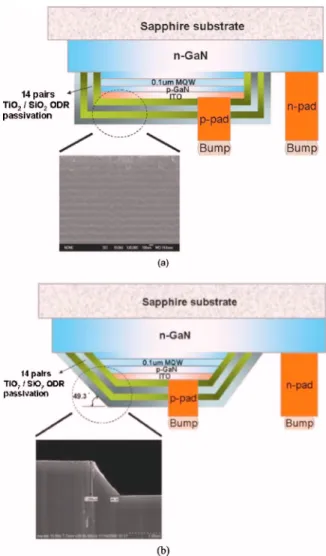
The schematic cross-sectional representations of the structures of InGaN/GaN vertical-injection LED coated ODRs we proposed are shown in Fig. 1a, with vertical sidewall, and Fig. 1b, with inclined sidewall. The GaN-based LED samples were grown by metallor-ganic chemical vapor deposition with a rotating-disk reactor 共Em-core兲 on a c-axis sapphire 共0001兲 substrate at the growth pressure of 200 mbar. The LED structure consists of a 50 nm thick GaN nucle-ation layer grown at 500°C, a 2m undoped GaN buffer, a 2 m Si-doped GaN buffer layer grown at 1050°C, an unintentionally doped InGaN/GaN MQW active region grown at 770°C, a 50 nm thick Mg-doped p-AlGaN electron blocking layer grown at 1050°C, a 0.25m thick Mg-doped p-GaN contact layer grown at 1050°C and a Si-doped InGaN/GaN short period superlattice struc-ture. The MQW active region consists of five periods of 3 nm/7 nm thick InGaN/GaN quantum well layers and barrier lay-ers. After annealing to activate Mg in the p-type layers, the FC ITO LEDs coated TiO2/SiO2ODR were fabricated using standard
pro-cess with a mesa area of 1⫻ 1 mm, the same as in Ref. 4. Figure 1a shows the schematic diagram of the FC ITO LED coated TiO2/SiO2ODR with vertical sidewall. We partially etched the surfaces of the LED samples using Cl2/Ar as the etching gas by
inductive-coupled-plasma reactive ion etching共ICP-RIE兲 until the n-type GaN layers were exposed. A 300 nm thick ITO layer was subsequently evaporated onto the sample surface by electron beam 共E-beam兲 evaporation for current spreading. The ITO layer had a high electrical conductivity共about 1.7 ⫻ 101⍀−1cm−1兲 and a high
transparency共⬎95% at 460 nm兲. Ti/Al/Ni/Au contacts were subse-quently deposited onto the exposed n-type GaN layers to serve as the n-type electrodes. SiO2layers were then deposited over all wa-fers by plasma enhanced chemical vapor deposition. Photolithogra-phy and HF solution etching were subsequently performed to define z
E-mail: [email protected]
Journal of The Electrochemical Society, 154共11兲 H944-H947 共2007兲 0013-4651/2007/154共11兲/H944/4/$20.00 © The Electrochemical Society
H944
) unless CC License in place (see abstract). ecsdl.org/site/terms_use
address. Redistribution subject to ECS terms of use (see 140.113.38.11
the P/N pad pattern for bump electroplating. The close-up scanning electron microscopy共SEM兲 image in Fig. 1a shows the step cover-age of the SiO2films which was well controlled to cover the entire
chips. Figure 1b depicts a schematic diagram of the FC ITO LED device coated TiO2/SiO2ODR with an inclined sidewall. Instead of
depositing TiO2/SiO2ODR on the mesa structure directly, an addi-tional etching process for FC ITO LEDs to form inclined sidewalls about 50° was carried out to mesa etching by using the ICP-RIE process. The inclined angle of the sidewall profile is defined as the angle between the horizontal line and sidewall. The inclined angle could be well controlled by using different ICP-RIE etching condi-tion. The inset of Fig. 1b shows the SEM picture of inclined side-walls profile of the FC ITO LED coated TiO2/SiO2ODR with an
inclined sidewall. It can be observed that the about 50° oblique inclined sidewall profile compared with initial etching mesa. Au80Sn20solder was used for electrical and mechanical interconnec-tion due to its very high reliability of good mechanical properties, good thermal conductivity, and low growth of intermetallic phase. Au80/Sn20共1600/400 nm兲 layers were then evaporated onto both FC
ITO LED device coated TiO2/SiO2ODR with vertical and inclined
sidewall samples while P/N bumps were defined by the lift-off pro-cess. During the bonding process, chips were picked, orientated, and flipped by a die bonder system. The FC ITO LED was soldered onto an AlN submount. For comparison reasons, both FC ITO LED
de-vices coated TiO2/SiO2 ODR with vertical and inclined sidewall were fabricated from exactly the same epitaxial wafer with the same chip size.
In this paper, the TiO2/SiO2ODR structure is similar to Ref. 4.
An ODR with 14 pairs of TiO2/SiO2共as shown in inset of Fig. 1b
for a SEM picture兲, was evaporated onto both samples by an E-beam evaporator at 150°C, and at an oxygen partial pressure of 2 ⫻ 10−4Torr with Ar and O
2as the ion source inlet gases. The film
deposition rates of TiO2and SiO2were 0.4 and 0.8 nm/s,
respec-tively. By the modal transmission-line method12 to calculate the various thicknesses as shown in Fig. 2, we found the most optimal CPBG at frequencies between 0.282 c/a and 0.304 c/a, where c is the speed of light and a is the lattice constant. We chose the lattice constant a = 133 nm to give a CPBG centered at 465 nm. Thus we found that our TiO2/SiO2ODR has a CPBG from 437 to 472 nm if
the thickness of TiO2and SiO2layers were chosen as 56 and 77 nm, respectively. We observed that rather low transmission共⬍0.05%兲 can be achieved from 441 to 465 nm from the angle dependent
Figure 1. 共Color online兲 Schematic diagram of the GaN-based FC ITO
LEDs共a兲 containing the TiO2/SiO2ODR, and共b兲 with ⬃50° inclined angle
coated TiO2/SiO2 ODR. The inset shows the SEM picture of the ⬃50°
inclined sidewall profile.
Figure 2. 共Color online兲 Photonic band structure diagram of a 1D PC
com-posed of TiO2and SiO2multilayers. Refractive indexes and layer thickness
are assumed to be n1= 2.52, d1= 56 nm for TiO2, and n2= 1.48, d2
= 77 nm for SiO2. The green and white regions distinguish between the
allowed and forbidden photon states, respectively. The region with yellow area of the complete photonic bandgap共CPBG兲 represents an omnidirec-tional reflection region.
Figure 3. 共Color online兲 Measurement transmittance results of the four
transmittance curves with different incidence angles共e.g., 0°, 30°, 60°, 85°兲 for unpolarized light vs wavelength.
H945
Journal of The Electrochemical Society, 154共11兲 H944-H947 共2007兲 H945
) unless CC License in place (see abstract). ecsdl.org/site/terms_use
address. Redistribution subject to ECS terms of use (see 140.113.38.11
transmission measurements. Figure 3 shows the measured transmit-tance at incidence angles of 0°, 30°, 60°, and 85° for unpolarized light as a function of the wavelength. We observed that rather high reflectance共⬎99.5%兲 can be achieved from 441 to 465 nm, and up to an incidence angle of 85°共e.g., the yellow region兲. This wave-length region falls in the CPBG shown in Fig. 3 and is expected from the photonic band diagram in Fig. 2.
Results and Discussion
We performed electroluminescence measurements by injecting a continuous current into our LEDs at room temperature. The light output was detected by a calibrated integrating sphere with Si pho-todiode on the package device. We found that the measured forward voltages under injection current 350 mA at room temperature for the FC ITO LED device coated TiO2/SiO2ODR with vertical and in-clined sidewall and the conventional face up ITO LED were all about 3.4 V. It was also found that the I-V curves were almost identical for the FC ITO LED coated TiO2/SiO2ODR with vertical
and inclined sidewall.
The intensity-current共L-I兲 characteristics of the three different types of LEDs were shown in Fig. 4. We clearly observed that the light output power of the FC ITO LED coated TiO2/SiO2ODR with
the inclined sidewall was larger than that with vertical sidewall un-der all driving currents. At an injection current of 350 mA, we found that the MQW emission peaks of those three different devices were all located at about 465 nm, and the light output power of the FC ITO LED coated TiO2/SiO2ODR with vertical and inclined side-wall and the conventional face up ITO LED were approximately
183, 158, and 83 mW, respectively. In other words, the FC ITO LED coated TiO2/SiO2 ODR with inclined and vertical sidewall
show the light output power enhancement by 122% and 92%, re-spectively, when compared to the conventional face up ITO LED. The FC ITO LED coated TiO2/SiO2ODR with an inclined sidewall
increased the light output power by a factor of 1.15 more than the device with vertical sidewall. It indicated that the FC ITO LED coated TiO2/SiO2ODR with about 50° inclined sidewall had better
light extraction efficiency than that with vertical sidewall.
We also measured the light output radiation patterns of the FC ITO LED coated TiO2/SiO2ODR with vertical and inclined side-walls at a driving current of 350 mA, as shown in Fig. 5. We mounted both structures on the header only and without epoxy
pack-Table I. Parameters of structure layer in the simulated GaN-based FC ITO LEDs with TiO2/SiO2ODR.
Layer Sapphire n-GaN MQW p-GaN ITO TiO2 SiO2
Thickness
共m兲 100 2.0 0.1 0.25 0.2 0.056 0.077
Refractive index
1.63 2.5 2.3 2.5 2.0 2.52 1.48
Figure 4.共Color online兲 EL intensity-current 共L-I兲 characteristics of the FC
ITO LEDs with an inclined sidewall coated TiO2/SiO2ODR, FC ITO LEDs with TiO2/SiO2ODR and conventional face up ITO LEDs, respectively.
Figure 5.共Color online兲 Measurements of the far-field patterns distribution
from the FC ITO LEDs with an inclined sidewall coated TiO2/SiO2 ODR
and the FC ITO LEDs with TiO2/SiO2ODR, respectively.
Figure 6. 共Color online兲 Top-view ray tracing images of the 共a兲 FC ITO
LED with an inclined sidewall coated ODR and共b兲 FC ITO LED with ODR.
H946 Journal of The Electrochemical Society, 154共11兲 H944-H947 共2007兲
H946
) unless CC License in place (see abstract). ecsdl.org/site/terms_use
address. Redistribution subject to ECS terms of use (see 140.113.38.11
age. Then the far-field pattern was measured from 0° to 180° by the conventional goniometric radiometer measurement technique. It can be seen that the FC ITO TiO2/SiO2ODR LED with inclined
side-wall shows higher extraction efficiency with a view angle about 150° than the LED with vertical sidewall. This enhancement is at-tributed to the higher reflectance of TiO2/SiO2ODR coated on
in-clined sidewall within the blue regime when compared to TiO2/SiO2
ODR coated on vertical sidewall.
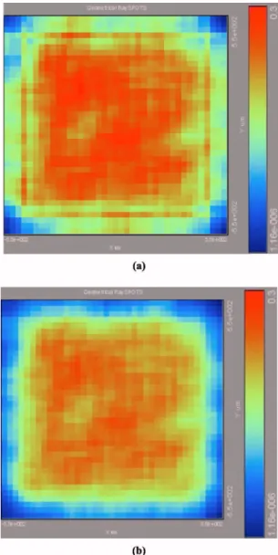
We also simulated the light propagation and reflection using the ray tracing method provided by Advanced System Analysis program software共ASAP兲. For simplicity, we employed a three-dimensional model on both GaN-based FC ITO TiO2/SiO2ODR LED with
ver-tical and with about 50° inclined sidewall. In addition, the simula-tion structure neglected sidewalls roughness and the absorpsimula-tion co-efficient. The relative thickness and refractive index of each structure layer of the simulated GaN-based FC ITO TiO2/SiO2ODR
LEDs are described in Table I. The top mesa area of both FC ITO LEDs was 1⫻ 1 mm. Figures 6a and b show the top-view ray tracing images of FC ITO TiO2/SiO2ODR LED with inclined and vertical sidewall, respectively. The x and y axes correspond to the chip length, 1⫻ 1 mm, and the color represents the light intensity. The result also shows the light extraction efficiency can be greatly enhanced by the inclined sidewall. Such an enhancement could have a larger probability to be scattered from the inclined sidewall and, thus, achieve high brighter LEDs.
Conclusion
In conclusion, GaN-based FC ITO TiO2/SiO2ODR LEDs with
an inclined sidewall were designed and fabricated. At a driving cur-rent of 350 mA and a chip size of 1⫻ 1 mm, the light output power and the light extraction enhancement of FC ITO TiO2/SiO2ODR LEDs with an inclined sidewall reaches 183 mW and an enhance-ment of 30% when compared to the same device without the in-clined sidewall. Furthermore, stronger enhancement around the
ver-tical direction and wider view angle as shown in the radiation patterns of the FC ITO TiO2/SiO2ODR LED with inclined sidewall
showed stronger optical power within 150° cone due to the higher reflectance and the inclined sidewall of the designed ODR within blue regime. Our work offers promising potential for enhancing out-put powers of commercial light emitting devices.
Acknowledgments
This work was supported by the National Science Council of the Republic of China共ROC兲 in Taiwan under contract no. NSC 94-2120-M009-007 and NSC 94-2752-E009-007-PAE.
National Chiao Tung University assisted in meeting the publication costs of this article.
References
1. M. Koike, N. Shibata, H. Kato, and Y. Takahashi, IEEE J. Sel. Top. Quantum Electron., 8, 271共2002兲.
2. J. K. Kim, Th. Gessmann, H. Luo, and E. F. Schubert, Appl. Phys. Lett., 84, 4508 共2004兲.
3. S. J. Chang, C. S. Chang, Y. K. Su, C. T. Lee, W. S. Chen, C. F. Shen, Y. P. Hsu, S. C. Shei, and H. M. Lo, IEEE Trans. Adv. Packag., 28, 273共2005兲. 4. C. H. Lin, C. F. Lai, T. S. Ko, H. W. Huang, H. C. Kuo, Y. Y. Hung, K. M. Leung,
C. C. Yu, R. J. Tsai, C. K. Lee, T. C. Lu, and S. C. Wang, IEEE Photon. Technol. Lett., 18, 2050共2006兲.
5. C. S. Chang, S. J. Chang, Y. K. Su, C. T. Lee, Y. C. Lin, W. C. Lai, S. C. Shei, J. C. Ke, and H. M. Lo, IEEE Photon. Technol. Lett., 16, 750共2004兲.
6. C. C. Kao, H. C. Kuo, H. W. Huang, J. T. Chu, Y. C. Peng, Y. L. Hsieh, C. Y. Luo, C. C. Yu, C. F. Lin, and S. C. Wang, IEEE Photon. Technol. Lett., 17, 19共2005兲. 7. C. F. Lin, Z. J. Yang, J. H. Zheng, and J. J. Dai, IEEE Photon. Technol. Lett., 17,
2038共2005兲.
8. C. F. Lin, Z. J. Yang, B. H. Chin, J. H. Zheng, J. J. Dai, B. C. Shieh, and C. C. Chang, J. Electrochem. Soc., 153, G1020共2006兲.
9. J. C. Bhat, M. J. Ludowise, and D. A. Steigerwald, U.S. Pat. 6,891,197B2共2005兲. 10. J. Q. Xi, M. Ojha, J. L. Plawsky, W. N. Gill, J. K. Kim, and E. F. Schubert, Appl.
Phys. Lett., 87, 031111共2005兲.
11. C. H. Lin, J. Y. Tsai, C. C. Kao, H. C. Kuo, C. C. Yu, J. R. Lo, and K. M. Leung, Jpn. J. Appl. Phys., Part 1, 45, 1591共2006兲.
12. C. H. Lin, K. M. Leung, and T. Tamir, J. Opt. Soc. Am. A, 19, 2005共2002兲.
H947
Journal of The Electrochemical Society, 154共11兲 H944-H947 共2007兲 H947
) unless CC License in place (see abstract). ecsdl.org/site/terms_use
address. Redistribution subject to ECS terms of use (see 140.113.38.11