1568 IEEE JOURNAL OF SOLID-STATE CIRCUITS, VOL. 47, NO. 7, JULY 2012
An Embedded Dynamic Voltage Scaling (DVS)
System Through 55 nm Single-Inductor Dual-Output
(SIDO) Switching Converter for 12-Bit Video
Digital-to-Analog Converter
Wen-Shen Chou, Tzu-Chi Huang, Student Member, IEEE, Yu-Huei Lee, Student Member, IEEE,
Yao-Yi Yang, Student Member, IEEE, Yi-Ping Su, Ke-Horng Chen, Senior Member, IEEE, Chen-Chih Huang,
Ying-Hsi Lin, Chao-Cheng Lee, Kuei-Ann Wen, Senior Member, IEEE, Ying-Chih Hsu, Yung-Chow Peng, and
Fu-Lung Hsueh
Abstract—This paper proposes a 55 nm CMOS 12-bit cur-rent-steering video digital-to-analog converter (DAC) directly powered by the single-inductor dual-output (SIDO) switching converter to compose a dynamic voltage scaling (DVS) system and improve the power efficiency. Dual-DVS control in both digital and analog circuits can effectively reduce power consumption. With various supply voltages, the video DAC can meet several different specifications in the power optimized (PO) mode. Fur-thermore, for DAC, the proposed 3S method, including finger separating, splitting and shifting, achieves good differential non-linearity (DNL) performance to 0.78/0.4 least significant bit (LSB) and integral nonlinearity (INL) 1.3/1.0 LSB (with/without SIDO converter) without additional calibration. It also suppresses the switching noise interference from the SIDO converter. Moreover, for SIDO converter, the cross-regulation performance is greatly improved in both transient and steady state to achieve lowest interference for the analog supply. The total power efficiency can be improved up to 11.5% and 28% in the DVS and the PO mode. The SIDO supplied DAC with the dual-DVS function achieves 69.88 dB spurious free dynamic range (SFDR) at the 1 V output swing and 1 MHz input. The proposed intrinsic 12-bit DAC and SIDO converter achieve high definition video DAC performance with the benefit of area and energy efficiency.
Index Terms—Single-inductor dual-output (SIDO), digital to analog converter (DAC), DC-DC converter, dynamic voltage scaling (DVS), least significant bit (LSB), differential nonlinearity (DNL), integral nonlinearity (INL), spurious free dynamic range (SFDR).
I. INTRODUCTION
I
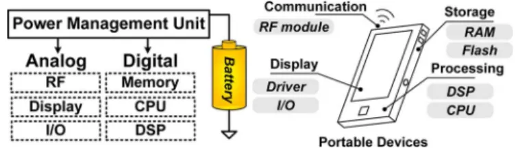
N RECENT years, the integrated circuits in nanometer technology have tailored for very high density dig-ital and mixed-signal integration applications. The trends of system-on-a-chip (SoC) integration lead the progress of portable devices to combine all the multimedia, communi-cation, storage and processing functions as shown in Fig. 1.Manuscript received November 14, 2011; revised January 31, 2012; accepted February 21, 2012. Daate of current version June 21, 2012. This paper was approved by Guest Editor Atila Alvandpour. This work was supported by the National Science Council, Taiwan, under Grant NSC 100-2220-E-009-050 and NSC 100-2220-E-009-055.
The authors are with the Department of Electronics Engineering, National Chiao Tung University, Hsinchu, Taiwan.
Color versions of one or more of the figures in this paper are available online at http://ieeexplore.ieee.org.
Digital Object Identifier 10.1109/JSSC.2012.2191331
Fig. 1. The system structure of a portable device.
Such a circuitry system can be roughly divided into digital and analog circuits. The digital circuits switch the voltage level up to supply voltage and down to the ground with high noise immunity. Remarkable improvements in the power con-sumption were achieved by the embedded power management unit (PMU), especially in nanometer technology SoC design with sub-1 V core devices. The PMU is often designed to fulfill different power requirements of each sub-circuit. Using input/output (I/O) devices with high-voltage tolerance can ensure the chip to be powered by the Li-Ion battery.
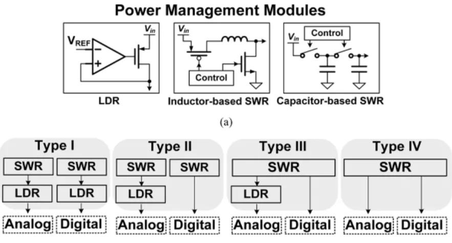
Low dropout regulators (LDRs) and switching regulators (SWRs) are two typical power modules in the design of embedded PMU [1] as shown in Fig. 2. LDRs possess the advantages of low noise and fast response, but suffer low efficiency once there is large dropout voltage. On the contrary, SWRs, which include the inductor-based and capacitor-based converters, have high conversion efficiency over a wide voltage range at the cost of output voltage ripple. Besides, the switching ripple will be coupled or fed into the circuits so as to influence the accuracy and quality of signals. As a result, the noise-sen-sitive analog circuit is often supplied by the LDRs, which behave as the post-regulators. There are different combinations of power modules as in Fig. 2(b), which depends on the system requirements. In Type I power module, the SWR is placed in front of the LDR to avoid large power loss caused by the dropout voltage in the LDR. For both analog and digital circuits with different supply voltage, two SWRs are needed at the cost of large number of external passive inductors or capacitors. Because digital circuit is not sensitive to noise, it can be di-rectly supplied by the SWR as Type II with high efficiency. To improve the integration performance, only one SWR is used to simultaneously supply multiple outputs for further reducing the
CHOU et al.: A DVS SYSTEM THROUGH 55 nm SIDO SWITCHING CONVERTER FOR 12-BIT VIDEO DAC 1569
Fig. 2. (a) The structure of different power modules. (b) Combination of power modules.
number of external components and the area of printed-circuit board (PCB) as the Type III. The SWR can be single-inductor multiple-output (SIMO) converter [2]–[4] to replace the use of many different types of SWR for high integration. Specially, careful design in analog circuit and the SIMO converter can further remove the demand of the LDR as depicted in the Type IV design. In this paper, the Type IV design is proposed to show the possible PMU implementation in high integration of SoC without suffering large chip area, external components and low power efficiency. Furthermore, the analog blocks in the SoC can also be supplied by the SWR if the performance, like voltage ripple, line/load regulation, and driving capability, can be improved.
From above demands, the SIMO DC-DC converter [2]–[4], which uses only one inductor, is an appropriate PMU solution. Minimization of external components achieves compact size and simultaneously provides two output voltages to different circuit blocks. Besides, the benefit of high efficiency can be guaranteed due to the characteristics of switching converters. The noise immunity in the analog blocks and the cross-regu-lation in the SIMO converter need to be carefully enhanced to meet the power requirements.
Furthermore, owing to finite power supplies in portable de-vices, it is imperative to have an integrated PMU with the dy-namic voltage scaling (DVS) [5], [6] methodology in digital circuits. Scaling the supply voltage can reduce the power con-sumption in different operation status. As we known, the DVS technique was seldom implemented in the analog blocks due to the deteriorated performance caused by the reduced voltage headroom. The analog circuits are sometimes more power-con-suming than the digital blocks. Thus, the DVS technique can also be implemented in some specific analog circuits with a great power reduction for system sustainability. The battery life can be further extended due to the removal of the LDRs and the implementation of the analog DVS technique. Dual-DVS technique is implemented in the proposed DVS system which includes an embedded power module (SIDO converter) and a mixed-signal circuit to show the energy-efficient and area-effi-cient performance compared to the prior arts. In this paper, to prove the feasibility of dual-DVS on both digital and analog circuits, an application of high quality video digital-to-analog
converter (DAC) circuit [7], [8], is taken into the system design, which is composed of digital control circuits and high accuracy analog circuit. The proposed 55 nm CMOS intrinsic 12-bit video DAC directly powered by the SIDO converter can simultane-ously achieve high performance and efficiency in various opera-tion modes through the implementaopera-tion of dual-DVS technique. That is, the dual-DVS technique can be fully implemented in the SoC with remarkable improvement on power efficiency to demonstrate its benefit in portable device applications.
The paper is organized as follows. The structure of DVS system is depicted in Section II. Section III illustrates the proposed 12-bit video DAC and the physical implementation. The proposed SIDO DC-DC converter and the DVS power optimization are described in Section IV. Experimental results are shown in Section V. Finally, a conclusion is drawn in Section VI.
II. STRUCTURE OFDYNAMICVOLTAGESCALINGSYSTEM
Recently, with the progress of storage and signal processing, high definition (HD) video and audio formats have become more and more popular in home appliances. Meanwhile, the advanced display technology on liquid crystal display (LCD) also improves the color gradation and response time on panels. Thus, high quality multimedia entertainment leads the prosperity of appliance and media industry. Conventional interfaces such as “true color” [9] are defined as that at least 256 shades of red, green, and blue (RGB), for a total of at least 16,777,216 color variations. It has been upgraded to higher pixels and finer resolution formats beyond “true color” such as HD video. There is also other display formats such as Y CbCr [10], which needs higher resolution than 8-bit in luminance(Y). The specifications of a video DAC should also be upgraded in both resolution and data rate. For example, the video DAC in blue-ray HD video players needs 12-bit resolution with the data rate of 150 MHz [7]. The portable devices also follow the trends of HD multimedia with more concerns on compact size and high power efficiency.
For a video DAC, there are many different component inter-faces [11] as shown in Fig. 3. The output voltage varies in dif-ferent ranges in difdif-ferent video interfaces. Such as in the Pb/Pr channel of Never The Same Color (NTSC) interface, the output
1570 IEEE JOURNAL OF SOLID-STATE CIRCUITS, VOL. 47, NO. 7, JULY 2012
Fig. 3. Different video interface applications and Signal range.
Fig. 4. (a) The structure of the video DAC. (b) Standard double terminal load of video DAC.
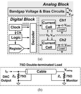
voltage difference is 0.7 V or 1 V. In the Y channel of Phase Alternating Line (PAL) interface, the output voltage difference is 0.5 V or 0.7 V. The synchronization voltage level can reset the pixel with an additional synchronization circuit. The video DAC needs the synchronization process in some applications. As a result, the total video DAC output voltage range may ex-tend to 1.3 V [11]. The video DAC in Fig. 4(a) is designed to meet several different video interface specifications [10]. Each video DAC has several output channels depending on the appli-cation. The standard output loading is shown in Fig. 4(b) which is the double-terminated load of 75 . The video DAC needs to have direct driving capability and large current delivering ability to generate large output swing on the load resistor. Thus the current-steering DAC architecture is chosen for benefiting both large current driving capability and high operation speed. The video DAC has both digital and analog circuits. Digital circuits include the clock generator, decoder and control logic. Analog circuits include the current cell array and the bandgap reference circuit which generates the bias voltage.
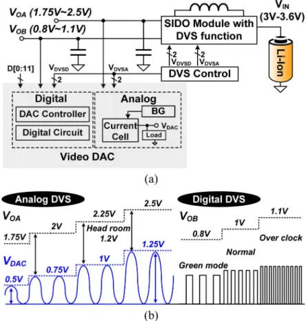
Fig. 5(a) shows the system architecture of the 12-bit video DAC with the DVS controller commanded by external con-trol signals, and , which also control the SIDO converter. Here, the SIDO switching DC-DC converter, sup-plied by the Li-Ion battery, will generate two voltage levels: and . The , ranging from 1.75 V to 2.5 V, can supply the analog circuits. The , with the range from 0.8 V to 1.1 V, drives the digital circuits of the video DAC which is implemented by low-voltage core devices in nanometer (nm) process. The digital input code [0:11] will be transferred to the analog output voltage . The DVS controller sends two two-bit signals and to determine dynamic analog and digital voltages, respectively. Through the DVS con-trol, the is selected from different full scale range from 500 mV to 1.3 V for various output requirements. Meanwhile, the SIDO converter will dynamically adjust the supply voltage to optimize the power consumption as shown in Fig. 5(b). III. PROPOSED12-BITCURRENTSTEERINGVIDEODAC
WITHDVS SCHEME
A. Structure and Operating Principle
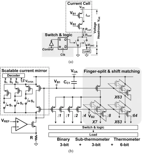
To successfully separate the 12-bit (4096) different color levels in high-definition video applications, the key perfor-mance index (KPI) of the video DAC is the linearity, especially for differential nonlinearity (DNL). The intrinsic 12-bit video DAC specifications include DNL 1 LSB and integral non-linearity (INL) 2 LSB with the maximum clock frequency 150 MHz for 1080 pixels HD video display application. The current cell mismatch, including both global and local varia-tion, will impact the video DAC performance. The proposed current cell with a cascode current mirror and switch logic is depicted in Fig. 6(a). By steering the output current to load resistor or GND, the DAC can generate output voltage level according to the digital input. The segmented architecture is commonly used to achieve high linearity current cell array, and the effects of unary and binary segmentation on the DNL and INL performances were studied in the literatures [8], [12]. The DNL is strongly affected by the segmentation scheme. Higher unary segmentation produces better DNL performance. On the other hand, the current cell array area will increase in the unary
CHOU et al.: A DVS SYSTEM THROUGH 55 nm SIDO SWITCHING CONVERTER FOR 12-BIT VIDEO DAC 1571
Fig. 5. (a) The structure of proposed DVS system. (b) The relationship of dual-DVS function.
segmentation. Higher binary segmentation achieves smaller DAC layout area.
To leverage the advantages of both unary and binary architec-tures, the segmentation of the 12-bit DAC is 6-bit thermometer code for the most-significant-bit (MSB) cells, 3-bit thermometer code for sub-MSB cells, and 3-bit binary LSB cells, as shown in Fig. 6(b). The 3-bit sub-MSB is adopted by thermometer de-coding to avoid mismatches in higher sub-MSB bits. Comparing with 6-bit binary LSB decoding, the 3-bit binary LSB and 3-bit thermometer sub-MSB can achieve better linearity due to the unary sub-MSB cells. As illustrated in Fig. 7, the main area of the DAC layout is in the 6-bit MSB array. The 3 + 3 sub-MSB and LSB only occupy a small portion of the total area. As a result, the “6 + 3 + 3” structure successfully achieves better lin-earity, and is of comparable area with “6 + 6” architecture.
To improve the DAC’s dynamic performance [13], the output impedance of the current cell must be large enough to func-tion as a good Norton equivalent current source [14]. The cur-rent-steering DAC’s spurious free dynamic range (SFDR) is approximated by (1). The is the output impedance of a single cascode current cell, the represents the load resis-tance, and is the resolution of the DAC. Through the standard double-terminated load and the SFDR requirements of 75 dB, the theoretical resistance value of is about 200 M . The proposed in a single current cell is over 250 M .
(1)
The wide-swing cascoded current-bias architecture improves the PSRR of the DAC. The use of noise coupling capacitor is to suppress the switching noise interference from the SIDO converter. In this design, the full-scale output current is 34 mA. At the equivalent resistive load of 37.5 , the max-imum output voltage is 1.3 V. Each MSB current cell will de-liver 0.541 mA output current. The scalable current mirror can adjust the mirror current according to the DVS control signal, , and generate various output swings depends on the system applications. Controlling the dynamic scaling voltage provided by the DC-DC SIDO converter and the DAC output full-scale voltage, the voltage headroom of the video DAC can be optimized for better performance and less power dissipation.
B. Physical Implementation of the 3S Method and Noise Suppression
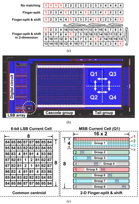
The physical implementation of the current cell array intro-duces the finger-split, shift and separate (3S) layout method. To reduce the steering current mismatch, the finger-split and shift technique, which is a two-dimensional matching layout as shown in Fig. 7(a). Compared with the conventional finger-split matching method, the proposed finger-split and shift method can further randomize the placement of the current cell to im-prove the linearity. In the physical implementation, the 12-bit control code is separated into two parts. The 3-bit least-signifi-cant-bit (LSB) current cell array and 3-bit sub-thermometer con-trol array are placed in common centroid layout as in Fig. 7(b).
1572 IEEE JOURNAL OF SOLID-STATE CIRCUITS, VOL. 47, NO. 7, JULY 2012
Fig. 6. (a) Single current cell and the switch. (b) Architecture of current cell in the 12-bit current steering DAC.
Fig. 7(c) shows the layout arrangement. The 6-bit MSB cur-rent cell array is placed by the finger-split and shift method. Each MSB current cell has 64 units of LSB current cell. The MSB array has been divided into 4 quadrants for the matching purpose, each quadrant has 16 fingers of each MSB cell as in Fig. 7(b). Sixteen fingers in a quadrant are separated in 8 groups by putting two cells together. The drain and source terminals of each cell can be shared to reduce large layout and routing area. The two-dimension finger-split and shift placement is ex-tended as depicted in Fig. 7(a) into 64 cells and called as a group. Thus, each group has 128 unit cells (16 2 4), the row and the column will shift by each group as illustrated in Figs. 7(b) and (c). Since the finger-split and shift technique is implemented cyclically, by mirroring the layout of each quadrant in two di-mensions, the layout complexity is reduced. As a result, it min-imizes the area penalty layout complexity. The tail group and cascode group use the same layout matching method.
The size of current source constituted by P-type MOSFET is chosen by the tradeoff between the mismatch and the silicon area. According to the Pelgrom MOSFET mismatch model as (2) [15], the current variation is related to two process parame-ters, and .
(2)
Refer to process mismatch parameters, is the process mismatch constant induced by MOSFET aspect ratio and other process parameters, e.g., mobility; is the threshold voltage variation constant. is the gate-source voltage and is the threshold voltage. To achieve performance-optimized design, the overdrive voltages of the current cells and the unit current are designed carefully to meet the mismatch require-ment at the largest output voltage swing of 1.3 V. According to Brownian-Bridge-Based statistical analysis, the 12-bit cur-rent-steering DAC should have relative standard deviation 0.24%, which corresponds to the INL smaller than 0.5 LSB [16]. By putting in the process mismatch parameter and the bias voltage , the minimum device size can be derived as m . For maximum output swing of 1.3 V, the LSB current is 8.3 A. Thus the selected current cell
device size is m and m.
In advanced CMOS technologies, there will be layout depen-dent effects (LDE), such as length of oxide-diffusion (LOD) and well proximity effects (WPE), which will impact the MOS array global variation performance. For large MSB array, the current cells will be more uniform at the center than at the corner. In the proposed 12-bit DAC layout, one surrounding ring of dummy current cells is added to prevent the layout-dependent effects. The more dummy cells were added, the smaller current mis-match between center and corner cells. However, it is at the cost of area overhead. The LDE (Layout Dependent Effect) will im-pact the current mismatch and result in worse DNL than those in
CHOU et al.: A DVS SYSTEM THROUGH 55 nm SIDO SWITCHING CONVERTER FOR 12-BIT VIDEO DAC 1573
Fig. 7. (a) Finger-split and shift method. (b) Layout of the DAC. (c) Layout arrangement.
theoretical results. Assuming symmetrical linear, symmetrical square and directional linear global variation as in Fig. 8(a), the mismatch of each current cell can be modeled by setting the current mismatch percentage of the center cell versus the corner cell (2% in this example). After applying 3S layout style, it can be seen that the finger-split and shift method achieves good matching performance of MSB array with DNL 0.15 LSB under all three different global variations. Compared with prior arts [17], [18], it shows worse linearity at symmetrical square condition ( 0.8 LSB) and better DNL at directional linear condition ( 0.06 LSB) as shown in Fig. 8(b). For large MOS arrays in advanced technology, it is more likely to have bowl-shape-like global variations due to the layout dependent effect. Besides, due to the cyclic property of finger-split and shift methodology, the 3S decoding sequence will not introduce large area overhead or layout complexity. In this work, the 1-ch DAC layout area is only 0.12 mm with 12-bit intrinsic linearity.
The optimized 3S decoding sequence can also minimize the sur-rounding dummy cell width because it can sustain larger center to corner current mismatch.
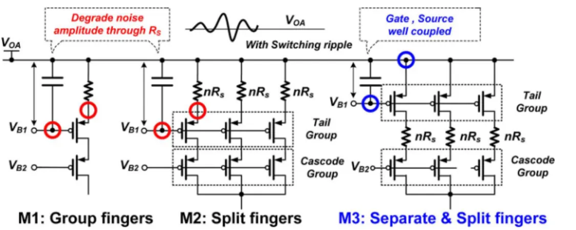
When the power source disturbances, it will impact the bias condition of the current cell and thus deteriorate the output current. As a result, the DNL and the INL will become worse when DVS is on and under power optimization mode. During the measurement, each current cell was turned on sequentially. If the power supply disturbed, the gate-source/drain-source voltage vary, the output current will also varies a little even under the power supply rejection. For high resolution and good signal quality, the power supply noise needs to be well handled not only from the circuit design, but also from the physical implementation. Fig. 9 shows three different matching manners of the 12-bit current-steering DAC architecture. To suppress the switching noise from the SIDO converter and current mismatch from the current steering control, the layout technique must
1574 IEEE JOURNAL OF SOLID-STATE CIRCUITS, VOL. 47, NO. 7, JULY 2012
Fig. 8. (a) Mismatch modeling. (b) Theoretical mismatch performance on current array.
Fig. 9. The finger-separate and split method.
be taken into consideration. In contrast to the original method which uses the group of finger, the prior method uses the splitting method to improve the current mismatching issue, while this kind of placement methods still suffers from switching noise interference due to the coupling effect on gate and source. The proposed method, , which adopts the split and separate method, separates the placement of tail group and cascade group in layout. It has lower the parasitic resistance between the tail group and power supply. Meanwhile, the switching noise from the SIDO converter can be suppressed and the 12-bit DAC with SIDO converter has less impact from
switching noise effect. The 3S method achieves good matching and noise immunity performance compared with the previous methods.
IV. SIDO CONVERTERWITHDVS POWEROPTIMIZATION
A. Proposed SIDO Converter
The proposed SIDO DC-DC converter in Fig. 10 provides two well-regulated voltages to analog blocks and digital circuits separately. The embedded DVS control can accept the external control signals, , to control the two feedback
CHOU et al.: A DVS SYSTEM THROUGH 55 nm SIDO SWITCHING CONVERTER FOR 12-BIT VIDEO DAC 1575
Fig. 10. The proposed SIDO converter with the couple circuit to reduce the cross-regulation for improving the SFDR of the 12-bit DAC.
Fig. 11. (a) Energy delivering sequence of the proposed SIDO converter. (b) Various deliver sequences.
voltages, and . Thus, the two DVS output voltages for power optimization can be accurately decided.
Only four power switches are used at the power stage which provides dual step-down outputs. The power switches, which are implemented by the thick oxide I/O devices in 55 nm CMOS technology, tolerate the voltage range
of battery-powered input up to 3.6 V. The voltage dividers are carried out by the DVS control to feed output voltage infor-mation back to the low-voltage (LV) controller for monitoring the two output loading conditions. Besides, the converter can operate both in the discontinuous conduction mode (DCM) and the continuous conduction mode (CCM) to improve the
1576 IEEE JOURNAL OF SOLID-STATE CIRCUITS, VOL. 47, NO. 7, JULY 2012
Fig. 12. The full-range current sense, summing circuit and timing diagrams.
Fig. 13. The proposed SIDO module for suppressing the switching noise to improve the SFDR of the 12-bit DAC.
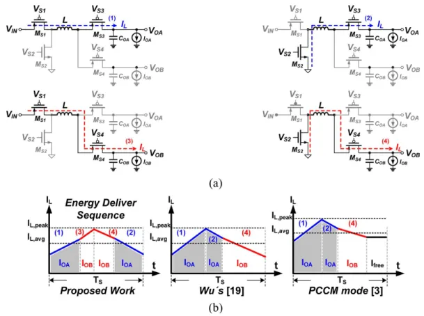
power efficiency over a wide load range. The pre-regulator generates a 1 V supply voltage and the reference for the LV-controller. Hence, the power consumption from the LV-controller can be decreased. The energy deliver sequences of the dual step-down SIDO converter are shown in Fig. 11(a). In phase (1) and phase (2), the inductor is in the charging state,
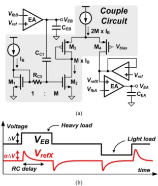
Fig. 14. (a) Proposed couple circuit for suppressing the cross-regulation. (b) Couple effect of the .
the SIDO converter delivers energy to both outputs and thus the inductor current rises. On the other hand, in phase (3) and phase (4), the inductor is in the discharging state and thus the inductor current falls. Compared to the prior arts as shown in
CHOU et al.: A DVS SYSTEM THROUGH 55 nm SIDO SWITCHING CONVERTER FOR 12-BIT VIDEO DAC 1577
Fig. 15. The measured ripple performance under different energy delivering sequence.
Fig. 16. The measured cross regulation in transient response.
Fig. 17. (a) Measurement of the DVS function. (b) Power efficiency of the SIDO converter.
Fig. 11(b), the Wu’s energy deliver sequence will limits the loading condition between the two outputs [19]. The freewheel stage in the pseudo-continuous conduction mode (PCCM) [2], [20], [21] occupies most of the switching period at light loads, and thereby resulting in low efficiency. In this work, to improve power conversion efficiency, the inductor current is effectively reduced by stacking the two inductor currents from the two outputs. Owing to the superposition, the overall
inductor current is simply equal to the summation of the two outputs as shown in Fig. 11(b). The two outputs are separately charged, which means the loading condition between two loads are not limited, and the inductor current can always be kept lower than those in the prior arts with PCCM technique.
The control scheme and the detail circuits are shown in Fig. 12. The current mode control loop is composed of the cur-rent sensing circuit, the voltage feedback loop and the summing
1578 IEEE JOURNAL OF SOLID-STATE CIRCUITS, VOL. 47, NO. 7, JULY 2012
Fig. 18. Measured DAC output swing and SFDR in the DVS mode.
Fig. 19. Measured DAC output swing and the SFDR in the PO mode.
Fig. 20. INL/DNL with/without the SIDO DVS supply.
circuit. The full-range current sensor can generate the sensing signal which is transformed from the inductor current in a certain ratio. The switches and will select the current signal according to the turn-on status of the power switches to achieve full-range current sense in each energy deliver path. The summing circuit will plus the with the ramp signal
, which is used to avoid sub-harmonic oscillation, and to implement the current-mode control. The and the are the error signals feedback from the outputs of the two error amplifiers. Hence, the and the represent the requested energy from both loads. The summed up represents the total energy requirements and should be compared with the
CHOU et al.: A DVS SYSTEM THROUGH 55 nm SIDO SWITCHING CONVERTER FOR 12-BIT VIDEO DAC 1579
Fig. 21. Measured DAC SFDR in the STD mode.
Fig. 22. Measured DAC SFDR in the DVS mode.
, which represents the energy in the inductor, to adjust the duty cycle for controlling the inductor current level. As the timing diagram depicted in Fig. 12, the energy will firstly deliver to the . When the reaches the , the receives enough energy and the energy will deliver to the until the reaches the . In the DCM operation, the CMOS controlled rectifier (CCR) and the zero current detection (ZCD) circuit in Fig. 10 control power MOSFETs to avoid reverse inductor current for high power conversion efficiency.
Furthermore, the energy delivery paths must be well arranged [2], [22], [23] and the cross-regulation needs to be carefully con-sidered at the same time. Cross-regulation is a well-known issue on the SIDO converters [19]–[25] and may take place in either transient or steady-state periods due to one-inductor utilization. To improve output quality on analog power supply, the SIDO converter operates in the analog ripple optimization condition. That is, the SIDO converter will deliver the energy to analog cir-cuits with high priority regardless the loading condition at the other output. Thus the voltage ripple on the can be mini-mized through suppressing the influence of power supply noise and optimizing the steady-state cross regulation.
Transient cross regulation was resulted from the energy de-livery scheme during the load transient response. If there is a sudden load change on the output as shown in Fig. 13(a), the needs more energy to cause the increase of the . As a result, the summed-up error signal will rise to increase the inductor current level. While the loading at the remains
the same, the energy delivered to will decrease due to the change of the sensing signal . Therefore, the voltage on will drop since less energy has been delivered to . On the contrary, the voltage will rise because receives more en-ergy as shown in Fig. 13(b).
Furthermore, the proposed SIDO converter includes the couple circuit to suppress the cross-regulation. In other words, the instant disturbance caused by one of the two outputs can be coupled to control the energy for minimizing the cross-reg-ulation. When the inductor current is firstly delivered to the analog output , a sudden load change on the will cause the to either drop or rise according to the polarity of load change [25]. The couple circuit as shown in Fig. 14(a) can couple the error signal generated from the error amplifier (EA) of the . Through the and the , the coupled signal will induce the discharging/charging effect and finely adjust the buffered reference voltage . The error signal will be influenced and change the duty cycle of the as shown in Fig. 14(b) to reduce the transient cross regulation of the . In other words, the cross-regulation can be effectively reduced.
B. DVS Power Optimization
For digital circuit, the supply voltage will influence the speed of the logic circuit. Thus the DVS function can adjust the supply voltage according to the operation frequency and achieve an op-timized performance and power consumption. For analog cir-cuit, voltage headroom and the bias voltage will be seriously
1580 IEEE JOURNAL OF SOLID-STATE CIRCUITS, VOL. 47, NO. 7, JULY 2012
TABLE I
DAC OPERATIONSTATUS ANDPERFORMANCE
Fig. 23. SFDR and power efficiency in different modes.
affected by the supply voltage. The voltage headroom influ-ences the resolution and linearity of the DAC [7], [8] and also dominates the power consumption of the whole system. Due to the various output swing and resolution requirements from dif-ferent video formats, the video DAC has difdif-ferent output sta-tuses. To provide various output swing and preserve the same signal quality of the analog blocks, the analog DVS control is in-troduced. Different display formats have to be defined by video processing unit or digital signal processor (DSP), and different supply voltage will be generated through SIDO converter once the DVS control circuits received the display information.
The DVS function is designed to save energy but also meet the requirement of the voltage headroom which guarantees the performance of the analog circuits. According to different output demands from 0.5 V to 1.3 V, the DVS controlled SIDO converter can provide appropriate supply voltage. For the bias and deep-saturation requirement of the cascode current cell, voltage headroom of 1.2 V is large enough to ensure good
Fig. 24. Chip micrograph.
TABLE II PERFORMANCESUMMARY
performance of the current cell. Thus the supply voltage is set to be 1.2 V higher than the voltage swing to minimize the unnecessary power loss caused by extra voltage headroom. The DVS function provides two different operation modes
CHOU et al.: A DVS SYSTEM THROUGH 55 nm SIDO SWITCHING CONVERTER FOR 12-BIT VIDEO DAC 1581
TABLE III
COMPARISONS OFOTHERDAC SYSTEMS
according to the video signal format. For low resolution re-quirements such as RGB outputs, the DVS module will enter the PO mode, which will keep the at the lowest output voltage of 1.75 V. Because the cascode current mirror, bandgap reference and OPAMP in the DAC circuits are designed by 2.5 V I/O devices, the supply voltage cannot be lower than 1.75 V to guarantee the correct operation of the DAC.
V. EXPERIMENTALRESULTS
The proposed 12-bit DAC supplied by the SIDO converter was fabricated in 55 nm CMOS process [29]. The SIDO module operates with an inductor of 4.7 H and two output capacitors of 4.7 F at 1 MHz switching frequency. The output ripple is less than 50 mV and the quiescent power of SIDO module con-troller is 120 W. The 12-bit DAC operates at 250 MHz clock frequency, with the input signal at 1 MHz.
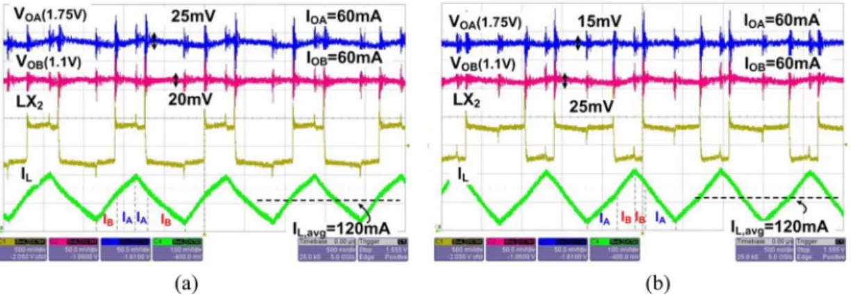
Fig. 15(a) shows the energy deliver sequence of the SIDO converter in the analog optimized condition and Fig. 15(b) shows the contrary deliver sequence at the same loading. The ripple in analog supply can be reduced from 25 mV to 15 mV, which optimizes the steady state cross regulation. Fig. 16(a) shows the transient cross regulation without the couple circuit. As the couple circuit starts operation, a better transient cross regulation performance can be achieved as in Fig. 16(b). Through the analog optimized delivering path and couple circuit, the switching ripple and the cross regulation in both steady state and transient can be minimized. The mea-sured DVS supply voltage is shown in Fig. 17(a). The power efficiency of the SIDO converter is shown in Fig. 17(b); the maximum power efficiency is 86%. Through the high efficiency
of SIDO converter with DVS control, the power efficiency can be optimized and extend the battery life of a portable device.
The SFDR of the 12-bit DAC and the power efficiency of the SIDO module via different full-scale output swing and supply voltage are shown in Fig. 18. The maximum SFDR is 69.88 dB at 1 V output. Here, a SFDR performance measurement result of the PO mode is provided for further power reduction but with the penalty of degrading some resolution as shown in Fig. 19. For large output swing up to 1.3 V, the headroom is not suf-ficiently large. Thus the output waveform suffers from some distortion resulting in degradation in the SFDR performance. Fig. 20 shows the INL and DNL performance with/without the SIDO DVS power supply. The switching noise of SIDO con-verter slightly degrades the DNL performance from 0.4 LSB to 0.78 LSB and the INL performance from 1 LSB to 1.3 LSB. The performance of DNL is smaller than 1 LSB. It demonstrates the correctness of intrinsic 12-bit video DAC with the DVS tech-nique and supplied by the SIDO converter. The SFDR of the DAC in STD mode and DVS mode under 75 MHz and 125 MHz are shown in Figs. 21 and 22, respectively.
The mode selection and the performance overview of the video DAC with/without SIDO module are in Fig. 23. The de-tails are also listed in Table I. The 12-bit video DAC supplied by LDR is called the standard (STD) condition. When supplied by SIDO converter, it presents the performance of both the DVS and the PO mode. We define the DAC power efficiency as the DAC output swing voltage divided by supply voltage, which represents the power wasting on the headroom requirement in analog circuits. The total power efficiency is defined as the DAC power efficiency multiplied by the power module’s efficiency. We assume a battery with 3.6 V output voltage as the system
1582 IEEE JOURNAL OF SOLID-STATE CIRCUITS, VOL. 47, NO. 7, JULY 2012
power supply in order to compare the differences between tra-ditional LDR and the proposed SIDO converter, as shown in Table I. It is observed that with the DVS control, the power efficiency can be promoted. In the PO mode, it also provides at least 60 dB of SFDR, which is capable for the traditional DVD quality video. Comparing with the tradition LDR solu-tion, the DAC supplied by the SIDO converter can save up to 11.5% and 28% of total power consumption in the DVS mode and the PO mode respectively. The chip micrograph is shown in Fig. 24. The total occupied silicon area is 1.335 mm (ex-cluding I/O cells and bond pads). The detailed design specifica-tions of both the SIDO converter and the video DAC are listed in Table II. Comparisons with other DAC methodologies are shown in Table III.
VI. CONCLUSION
In this paper, a 12-bit video DAC and the power supply SIDO converter module are proposed. The test chip was fabricated in 55 nm CMOS process. The SIDO DC-DC converter generates two high efficiency power outputs for different circuit blocks with only one power module which saves the PCB area and the quantity of external component. At 1 MHz input, without linear regulator, SIDO DC-DC converter with dual-DVS tech-nique improves the DAC’s total power efficiency up 11.5% and achieves maximum 69.88 dB SFDR in the DVS mode. The PO mode provides a solution for low power operation and still maintains the acceptable SFDR up to 60.94 dB and 68.4 dB at 1.3 V and 0.75 V output swing respectively. Through the mea-surement result, it is clear that the 3S method exhibits not only a better performance in matching issues but also in the noise re-duction theme. This combination is an area and energy efficient solution and will be valuable for many video applications such as the driver or controller of a monitor screen, which also in-cludes digital control circuits, DAC and I/O circuits.
ACKNOWLEDGMENT
The authors wish to thank TSMC for supporting the joint-development project.
REFERENCES
[1] Y.-H. Lee, Y.-Y. Yang, K.-H. Chen, Y.-H. Lin, S.-J. Wang, K.-L. Zheng, P.-F. Chen, C.-Y. Hsieh, Y.-Z. Ke, Y.-K. Chen, and C.-C. Huang, “A DVS embedded power management for high efficiency integrated SoC in UWB system,” IEEE J. Solid-State Circuits, vol. 45, no. 11, pp. 2227–2238, Nov. 2010.
[2] M.-H. Huang and K.-H. Chen, “Single-inductor multi-output (SIMO) DC-DC converters with high light-load efficiency and minimized cross-regulation for portable devices,” IEEE J. Solid-State Circuits, vol. 44, no. 4, pp. 1099–1111, Apr. 2009.
[3] D. Ma, W.-H. Ki, and C.-Y. Tsui, “A pseudo-CCM/DCM SIMO switching converter with freewheel switching,” IEEE J. Solid-State
Circuits, vol. 38, no. 6, pp. 1007–1014, June 2003.
[4] Y.-H. Lee, Y.-Y. Yang, S.-J. Wang, K.-H. Chen, Y.-H. Lin, Y.-K. Chen, and C.-C. Huang, “Interleaving energy-conservation mode (IECM) control in single-inductor dual-output (SIDO) step-down converters with 91% peak efficiency,” IEEE J. Solid-State Circuits, vol. 46, no. 4, pp. 904–915, Mar. 2011.
[5] S. Das, D. Roberts, S. Lee, S. Pant, D. Blaauw, T. Austin, K. Flautner, and T. Mudge, “A self-tuning DVS processor using delay-error detec-tion and correcdetec-tion,” IEEE J. Solid-State Circuits, vol. 41, no. 4, pp. 792–804, Apr. 2006.
[6] M. E. Sinangil, N. Verma, and A. P. Chandrakasan, “A reconfigurable 8 T ultra-dynamic voltage scalable (U-DVS) SRAM in 65 nm CMOS,” IEEE J. Solid-State Circuits, vol. 44, no. 11, pp. 3163–3173, Nov. 2009.
[7] Analog Device Inc., Multiformat SD, Progressive Scan/HDTV Video Encoder With Six 11-Bit DACs 2002, Analog Devices.
[8] J. Hyde, T. Humes, C. Diorio, M. Thomas, and M. Figueroa, “A 300-MS/s 14-bit digital-to-analog converter in logic CMOS,” IEEE J.
Solid-State Circuits, vol. 38, pp. 734–740, May 2003.
[9] Analog Device Inc., ADV7125 CMOS, 330 MHz, Triple 8-Bit High Speed Video DAC, 2011, Analog Devices.
[10] Texas Instruments Inc., THS8135 Triple 10-bit 240MSPS Video DAC With Tri-Level Sync and Video 2002, Texas Instruments.
[11] National Semiconductor Inc., LMH1981 Multi-Format Video Sync. Separator July 2007, National Semiconductor.
[12] J. Starzyk, R. Mohn, and L. Jing, “A cost-effective approach to the design and layout of a 14-bit current-steering DAC macrocell,” IEEE
Trans. Circuits Syst. I, vol. 51, pp. 196–200, Jan. 2004.
[13] A. Van den Bosch, M. Steyaert, and W. Sansen, “SFDR-bandwidth limitations for high speed high resolution current steering CMOS D/A converters,” in Proc. IEEE Int. Conf. Electronics, Circuits, and Systems
(ICECS), Sept. 1999, vol. 32, no. 12, pp. 1193–1196.
[14] J. J. Wikner and N. Tan, “Modeling of CMOS digital-to-analog con-verters for telecommunication,” IEEE Trans. Circuits Syst. II, vol. 46, no. 5, pp. 489–499, May 1999.
[15] M. J. M. Pelgrom, A. C. J. Duinmaijer, and A. P. G. Welbers, “Matching properties of MOS transistors,” IEEE J. Solid-State
Cir-cuits, vol. 24, pp. 1433–1440, Oct. 1989.
[16] G. I. Radulov, M. Heydenreich, R. W. van der Hofstad, J. A. Hegt, and A. H. M. van Roermund, “Brownian-bridge-based statistical analysis of the DAC INL caused by current mismatch,” IEEE Trans. Circuits
Syst. II, vol. 54, no. 2, pp. 489–499, Feb. 2007.
[17] C.-H. Lin and K. Bult, “A 10-b, 500-MSample/s CMOS DAC in 0.6 mm ,” IEEE J. Solid-State Circuits, vol. 33, no. 12, pp. 1948–1958, Dec. 1998.
[18] J. Deveugele and M. S. J. Steyaert, “A 10-bit 250-MS/s bi-nary-weighted current-steering DAC,” IEEE J. Solid-State Circuits, vol. 41, no. 2, pp. 320–329, Feb. 2006.
[19] W. Xu, Y. Li, X. Gong, Z. Hong, and D. Killat, “A dual-mode single-in-ductor dual-output switching converter with small ripple,” IEEE Trans.
Power Electron., vol. 25, no. 3, pp. 614–623, Mar. 2010.
[20] H.-P. Le, C.-S. Chae, K.-C. Lee, S.-W. Wang, G.-H. Cho, and G.-H. Cho, “A single-inductor switching DC-DC converter with five outputs and ordered power-distributive control,” IEEE J. Solid-State Circuits, vol. 42, no. 12, pp. 2076–2714, Dec. 2007.
[21] K.-S. Seol, Y.-J. Woo, G.-H. Cho, G.-H. Cho, J.-W. Lee, and S.-I. Kim, “Multiple-output step-up/down switching DC-DC converter with ves-tigial current control,” in IEEE ISSCC Dig. Tech. Papers, Feb. 2009, pp. 442–443.
[22] C.-S. Chae, H.-P. Le, K.-C. Lee, G.-H. Cho, and G.-H. Cho, “A single-inductor step-up DC-DC switching converter with bipolar outputs for active matrix OLED mobile display panels,” IEEE J. Solid-State
Cir-cuits, vol. 44, no. 2, pp. 509–524, Feb. 2009.
[23] M.-H. Huang, Y.-N. Tsai, and K.-H. Chen, “Sub-1 V input single-inductor dual-output (SIDO) DC-DC converter with adap-tive load-tracking control (ALTC) for single-cell-powered systems,”
IEEE Trans. Power Electron., vol. 25, no. 7, pp. 1713–1724, June
2010.
[24] Y.-H. Lee, T.-C. Huang, Y.-Y. Yang, K.-H. Chen, Y.-H. Lin, W.-S. Chou, C.-C. Huang, and Y.-K. Chen, “Minimized transient and steady-state cross regulation in 55 nm CMOS single-inductor dual-output (SIDO) step-down DC-DC converter,” in Proc. IEEE
Asian Solid-State Circuits Conf. (A-SSCC), Nov. 2010, pp. 65–68.
[25] Y.-H. Lee, T.-C. Huang, Y.-Y. Yang, K.-H. Chen, Y.-H. Lin, W.-S. Chou, C.-C. Huang, and Y.-K. Chen, “Minimized transient and steady-state cross regulation in 55 nm CMOS single-inductor dual-output (SIDO) step-down DC-DC converter,” IEEE J. Solid-State
Circuits, vol. 46, no. 11, pp. 2488–2499, Nov. 2011.
[26] M.-H. Shen and P.-C. Huang, “A low cost calibrated DAC for high-res-olution video display system,” IEEE Trans. Very Large Scale
Integra-tion Syst., Aug. 2011.
[27] T. Chen and G. Gielen, “A 14-bit 200-MHz current-steering DAC with switching-sequence post-adjustment calibration,” IEEE J. Solid-State
Circuits, vol. 42, no. 11, pp. 2386–2394, Nov. 2007.
[28] K. O’Sullivan, C. Gorman, M. Hennessy, and V. Callaghan, “A 12-bit 320-MSample/s current-steering CMOS D/A converter in 0.44 mm ,”
CHOU et al.: A DVS SYSTEM THROUGH 55 nm SIDO SWITCHING CONVERTER FOR 12-BIT VIDEO DAC 1583
[29] T.-C. Huang, W.-S. Chou, Y.-H. Lee, Y.-Y. Yang, K.-H. Chen, Y.-C. Peng, and F.-L. Hsueh, “55 nm CMOS 12-bit 250 MHz dig-ital-to-analog converter with dynamic voltage scaling (DVS) technique through single-inductor dual-output (SIDO) converter,” in Proc. IEEE
Euro. Solid-State Circuits Conf. (ESSCIRC), Sept. 2011, pp. 383–368.
Wen-Shen Chou was born in Taipei, Taiwan. He
received his B.S., and M.S. degrees in electrical engineering from National Taiwan University, Taipei, Taiwan, in 1994 and 1996 respectively. From 1996 to 1998, he served the military service in the army, Taiwan. From 1998 to 2002, he was a Process Integration Engineer in TSMC, Hsinchu, Taiwan. From 2003 to 2011, he was engaged in mixed-signal design in TSMC Design and Technology Platform. He is also a faculty member at the Mixed-Signal and Power Management IC Laboratory, Institute of Electrical Control Engineering, National Chiao Tung University, Hsinchu, Taiwan. He is currently pursuing the Ph.D. degree in the Institute of Electronic Engineering, National Chiao Tung University, Hsinchu, Taiwan. His research interests include high-speed digital-to-analog converter, power management integrated circuit and mixed-signal circuit designs.
Tzu-Chi Huang (S’11) was born in Hsinchu,
Taiwan. He received both B.S. and M.S. degrees from the Department of Electrical Engineering, National Cheng Kung University, Tainan, Taiwan. He is currently pursuing the Ph.D. degree at the Institute of Electrical Control Engineering, National Chiao Tung University, Hsinchu, Taiwan.
He is a faculty member at the Mixed-Signal and Power Management IC Laboratory, Institute of Elec-trical Control Engineering, National Chiao Tung Uni-versity, Hsinchu, Taiwan. He is currently working on low power energy harvesting system and power management circuit design. His research interests include the power management IC design, analog integrated circuits, and mixed signal IC design.
Yu-Huei Lee (S’09) was born in Taipei, Taiwan.
He received both B.S. and M.S. degrees from the Department of Electrical and Control Engineering, National Chiao Tung University, Hsinchu, Taiwan, in 2007 and 2009, respectively. He is currently pursuing the Ph.D. degree in the Institute of Elec-trical Control Engineering, National Chiao Tung University, Hsinchu, Taiwan.
He is a faculty member at the Mixed-Signal and Power Management IC Laboratory, Institute of Elec-trical Control Engineering, National Chiao Tung Uni-versity, Hsinchu, Taiwan. His current research interests include the power man-agement integrated circuit design, LED driver IC design, and analog integrated circuits.
Yao-Yi Yang (S’09) was born in Changhua, Taiwan.
He received the B.S. and M.S. degrees from Chung Yuan Christian University and National Taipei University of Technology in 2004 and 2007, respec-tively. He is currently pursuing the Ph.D. degree in the Institute of Electrical Control Engineering, National Chiao Tung University, Hsinchu, Taiwan.
He is a faculty member at the Mixed-Signal and Power Management IC Laboratory, Institute of Elec-trical Control Engineering, National Chiao Tung Uni-versity, Hsinchu, Taiwan. His research interests in-clude the power management IC design, LED driver IC design and, the analog integrated circuits.
Yi-Ping Su was born in Taipei, Taiwan. She received
the B.S. degree from the Department of Electrical Engineering, National Sun Yat-sen University, Kaoh-siung, Taiwan, in 2009. She is currently working to-ward the Ph.D. degree in the Institute of Electrical Engineering, National Chiao Tung University.
She is a faculty member at the Mixed-Signal and Power Management IC Laboratory, Institute of Elec-trical Control Engineering, National Chiao Tung Uni-versity, Hsinchu, Taiwan. Her current research inter-ests include the power management integrated cir-cuits design, battery charging integrated circir-cuits design, and analog integrated circuits design.
Ke-Horng Chen (M’04-SM’09) received the B.S.,
M.S., and Ph.D. degrees in electrical engineering from National Taiwan University, Taipei, Taiwan, in 1994, 1996, and 2003, respectively.
From 1996 to 1998, he was a part-time IC De-signer at Philips, Taipei, Taiwan. From 1998 to 2000, he was an Application Engineer at Avanti, Ltd., Taiwan. From 2000 to 2003, he was a Project Manager at ACARD, Ltd., where he was engaged in designing power management ICs. He is currently a Professor with the Department of Electrical Engi-neering, National Chiao Tung University, Hsinchu, Taiwan, where he organized a Mixed-Signal and Power Management IC Laboratory. He is the author or coauthor of more than 100 papers published in journals and conferences, and also holds several patents. His current research interests include power management ICs, mixed-signal circuit designs, display algorithm and driver designs of liquid crystal display (LCD) TV, red, green, and blue (RGB) color sequential backlight designs for optically compensated bend (OCB) panels, and low-voltage circuit designs.
Dr. Chen has served as an Associate Editor of the IEEE TRANSACTIONS ON POWER ELECTRONICS and IEEE TRANSACTIONS ON CIRCUITS AND SYSTEMS—PART II: EXPRESS BRIEFS. He is on the IEEE Circuits and Systems (CAS) VLSI Systems and Applications Technical Committee, and the IEEE CAS Power and Energy Circuits and Systems Technical Committee.
Chen-Chih Huang received the B.S. degree from
National Chiao-Tung University, Hsinchu, Taiwan, R.O.C., in 1990, and the M.S. degree in electrical en-gineering from National Taiwan University, Taipei, Taiwan, in 1992.
He joined Mosel Vitelic Inc., Hsinchu, as an engi-neer in 1994. In 1995, He joined Realtek Semicon-ductor Corp., Hsinchu, as an analog circuit design engineer. During 1995–2010, he was responsible for several projects including fast Ethernet/Gigabit Eth-ernet network interface controller/PHYceiver/switch controller, Clock generator, USB, ADSL router, Gateway controller, etc. He is currently the Senior Manager of Analog_CN design team of R&D center.
Ying-Hsi Lin received the B.S. degree from National
Chiao-Tung University, Hsinchu, Taiwan, R.O.C., in 1993, and the M.S. degree in electrical engineering from National Taiwan University in 1995.
He joined Computer & Communication Re-search Lab at ITRI, as a reRe-searcher in 1995, and became project leader of CMOS RF and high speed mixed-signal circuits design in 1998. Since joining ITRI CCL, he has been working on CMOS radio frequency integrated circuits and mixed-signal circuits IC design for computer and communication application. In October 1999, He joined Realtek Semiconductor Corp., as a RF manager, where he was responsible for several R&D CMOS RF projects including GPS, Bluetooth, WLAN 802.11abg, 802.11n, WLAN CE and UWB, and also involving CMOS RF IC mass production planning. In the circuits design, his activities ranged are RF synthesizer, LNA, Mixer, modulator, PA, filter, PGA, mixed-signal circuits, ESD circuits, RF device modeling, RF
1584 IEEE JOURNAL OF SOLID-STATE CIRCUITS, VOL. 47, NO. 7, JULY 2012
system calibration and communication system design. In 2009, he was pro-moted to vice president of Realtek Semi. Corp., and led the Research & Design Center of Realtek. He holds more than 40 patents in the area of mixed-signal and RF IC design. In 2009, he received an award “National Outstanding Manager in R&D Topic” from Chinese Professional Management Association.
Chao-Cheng Lee received the B.S. degree from
Na-tional Chiao-Tung University in 1988 in electrical en-gineering. And he received the M.S. degree from Na-tional Taiwan University in 1990 in physics.
He joined Realtek Semiconductor in 1992 and is currently the Senior Vice President of Engineering in Realtek. His research interests includes PLL, filter, high speed OP, mismatch calibration. He has more than 30 U.S. patents granted or pending.
Kuei-Ann Wen (M’90-SM’02) received the B.S.,
M.S., and Ph.D. degrees in electrical engineering from National Cheng-Kung University (NCKU), Taiwan, in 1983, 1985, and 1988, respectively. She is currently a full Professor in the Dept. of EE at National Chiao Tung University, Taiwan. Dr. Wen’s research interests are in the areas of SoC design and VLSI wireless communication circuit/system also including RF circuits and baseband design. She covers and enhances the curriculum for SoC integration, VLSI computing and signal processing, and RF wireless communication. She has been involved in several key research projects including advanced IC/VLSI for academic excellence, and technology transfer for successful high-tech. She also set up the research cooperation laboratories with Agilent, Mentor Graphics and Synopsys for the development of wireless SoC design automation as well as the flow for industrial experts. She leads the Transactions Wireless Technology (TWT) Laboratory sponsored by United Microelectronics Co. (UMC) for the development of advanced CMOS RF.
Ying-Chih Hsu was born in Taichung, Taiwan,
R.O.C., in 1981. He received the B.S. degree in electronics engineering from National Chiao-Tung University, Hsinchu, Taiwan, R.O.C., in 2003, and the M.S. degree in electronics engineering from National Taiwan University, Taipei, Taiwan, R.O.C., in 2005.
His research interests include RF integrated circuits and monolithic microwave integrated circuit (MMIC) designs.
Yung-Chow Peng was born in Hsinchu, Taiwan.
He received his B.S., and M.S. degrees in electrical engineering from National Cheng-Kung University and National Chiao-Tung University, Taiwan, in 1984 and 1986 respectively. From 1986 to 1993, he served the military RDSS service in ITRI/ERSO, Taiwan. From 1993 to 2005, he was a department manager for developing mix-signal products for per-sonal computer in Winbond, Hsinchu, Taiwan. From 2005 to 2007, he was a director in mixed-signal/RF division for set-top-box and DVD in Cheertech, Hsinchu. He is currently a deputy director in charge of device level test method-ology and mixed-signal test vehicles with sensitive serdes and analog building blocks in TSMC, Hsinchu, Taiwan. His research interests include high-speed serdes, advanced technology test vehicles and MEMS inertial sensors.
Fu-Lung Hsueh received the B.S. and M.S. degrees
from National Chiao-Tung University, Hsinchu, Taiwan, and the Ph.D. degree from Lehigh Univer-sity, Bethlehem, PA, all in electrical engineering.
He is the Director of Design Technology Division, Taiwan Semiconductor Manufacturing Company (TSMC), Hsinchu, Taiwan, and is a Fellow of the TSMC Academy. Prior to joining TSMC in 2003, he worked at Sarnoff Corporation (formerly RCA Research Center), Princeton, NJ, for 22 years. His major technical experiences include mixed-signal circuits, flat-panel display, and CMOS/CCD image sensor designs. Dr. Hsueh was the recipient of five Outstanding Technical Achievement Awards at Sarnoff, and three Chairman Innovation Awards at TSMC.