Improvements in Both Thermal Stability of Ni-Silicide and
Electrical Reliability of Gate Oxides Using a Stacked Polysilicon
Gate Structure
Jam Wem Lee, Shen-Xiang Lin, Tan-Fu Lei, and Chung-Len Lee
Department of Electronics Engineering, National Chiao Tung University, Hsinchu, Taiwan
A process design is presented for improving the thermal stability of Ni-silicide共nickel-silicide兲 using a stacked polysilicon gate structure. The Ni-silicide formed has low sheet resistance up to 800°C on a silicidation process. Additionally, the metal-oxide-semiconductor共MOS兲 capacitors fabricated using these proposed gate structures demonstrate higher electrical reliability for gate oxides than those of nonstacked films. That is, the gate oxides of the MOS capacitors were only slightly degraded after silicidation step at 800°C. In conclusion, the Ni-silicide formed on those stacked polysilicon gates are attractive in fabricating ultralarge scale integration共ULSI兲 circuits because both the thermal stability of Ni-silicide and the reliability of gate oxides are improved simultaneously.
© 2001 The Electrochemical Society. 关DOI: 10.1149/1.1392325兴 All rights reserved.
Manuscript submitted October 31, 2000; revised manuscript received April 11, 2001. Available electronically August 10, 2001.
Silicides coupled with heavily doped silicon films are widely used as low resistance gate electrodes and local interconnects. Among them, nickel-silicide共NiSi兲 can be formed at lower tempera-ture with small extent of silicon consumption as compared with both TiSi2and CoSi2.1Additionally, NiSi can maintain a thin and narrow silicide layer with low sheet resistance. However, the intrinsic prop-erties of NiSi film can be readily degraded during post-thermal processes.2-4 Thus, it is important to study the impact of post-thermal processes on NiSi’s post-thermal stability to preserve its perfor-mance in terms of low resistance.
The morphological degradation of Ni-silicide depends strongly on both the grain size and the relative thickness共silicide layer vs. polysilicon layer兲 of the underlying layer silicon.5-7 The thermal stability of silicide increases relatively, if the size of the silicon grain increases, the thickness of silicide increases, and the layer of silicon film grows thinner. Therefore, it is desirable to make Ni-silicide film reasonably thick to improve thermal stability and to possess the lowest series resistance. Meanwhile, thickness of silicon film should also be deposited reasonably thin to increase the thermal stability and to simplify the complexity of integrating the entire process. However, the thickness of those films should be carefully designed to prevent silicide protrusions from extending over the silicon film or penetrating into the gate oxide during subsequent thermal pro-cesses. To ensure the thermal stability of Ni-silicide and gate oxide reliability, it is important to design appropriate thickness of silicon and silicide in improving the thermal stability and suppressing Ni penetration.
To improve the thermal stability of Ni-silicide, the underlying layer silicon deposited using disilane gas was used here. Disilane has been favorably used in fabricating high-quality low-temperature thin-film transistors. The results in this experiment indicate that the Ni-silicide formed on this silicon film has higher thermal stability, but there is a lack of effect on suppressing Ni penetration. From the standpoint of suppressing Ni penetration, a film stack containing two silicon structures was constructed for the first time to attain both NiSi thermal stability and gate oxide reliability共suppressing Ni pen-etration兲 simultaneously. This film structure did improve both ther-mal stability and gate oxide reliability.
Experimental
n-Type共100兲 wafers were first grown with a 500 nm field oxide and patterned to isolate the devices. Then, all samples were Radio Corporation of America 共RCA兲 cleaned and grown with a 10 nm thermal oxide at 950°C in an O2ambient after the photoresist was stripped. Afterward, the wafers were deposited in a stacked silicon film 200 nm thick. There are two kinds of film stacks prepared in this experiment: 共i兲 DS sample, a 100 nm silicon film deposited using disilane gas at 460°C in low pressure chemical vapor deposi-tion共LPCVD兲 ambient followed by a 100 nm silicon film deposited
using silane gas at 620°C without exposing samples to atmosphere, and共ii兲 DA sample, a 100 nm silicon film deposited using disilane gas at 460°C in LPCVD ambient followed by a 100 nm silicon film deposited using silane gas at 550°C without exposing samples to atmosphere. In comparison, the 200 nm thick silicon films deposited using silane at 620°C共S兲 and 550°C 共A兲 along with film deposited using disilane at 460°C 共D兲 were also prepared. Furthermore, to study how the silicon film thickness affects the thermal stability of the Ni-silicide, silicon films, 100, 200, and 300 nm thick, respec-tively, were also prepared using silane at 620°C.
After silicon gate was deposited, the samples were then BF2 implanted with a dose of 5⫻ 1015/cm2at energy of 40 keV. These samples were then rapid thermal annealing共RTA兲 annealed at 950°C in an N2ambient for 30 s. Basically, all the films had been trans-formed into polycrystalline silicon with similar grain sizes by ob-serving images from transmission electron microscope共TEM兲. The samples were then RCA cleaned and a 30 nm Ni film was deposited using an electron-beam evaporator. Following the deposition of Ni, the samples were RTA annealed from 350 to 850°C in an N2ambient for 30 s. The selective chemical etcher (H2SO4:H2O2⫽ 3:1) was used to etch the remaining Ni without attacking Ni-silicide. Four-point probe was then used to measure the sheet resistance of the Ni-silicide thin film.
A 500 nm Al film was deposited on the Ni-silicide films. Alumi-num共Al兲, NiSi, and polysilicon films were then patterned to form the top electrodes共gate兲 of the metal-oxide-semiconductor 共MOS兲 capacitors. After native oxide at the back side was removed, a 500 nm Al film was deposited on the back side of the samples. Finally, all samples were sintered at 400°C in an N2ambient.
Results and Discussion
Figure 1 shows the average and error bars extracted from 20 points of measured sheet resistance of the Ni-silicide films, which were formed by depositing 30 nm Ni on six silicon substrates with various RTA temperatures. These six silicon substrates are described as follows:共i兲 S, 200 nm silicon film deposited using silane gas at 620°C,共ii兲 D, 200 nm silicon film deposited using disilane gas at 460°C,共iii兲 A, 200 nm silicon film deposited by silane gas at 550°C, (iv) c-Si, 共100兲 p-type crystalline silicon bulk, (v) DS, 100 nm D silicon film共underlayer兲 followed by depositing 100 nm S silicon film共upper layer兲, and (vi) DA, 100 nm D silicon film 共underlayer兲 followed by depositing 100 nm A silicon film共upper layer兲. The S and A samples have lower thermal stability than that of the D sample or the stacked samples.
The differences of thermal stability among S, A, and D samples can be explained by the X-ray diffraction pattern共XRD兲 profiles of the S, A, and D samples, all samples were BF2implanted and RTA annealed at 950°C for 30 s, as shown in Fig. 2. The profiles show Journal of The Electrochemical Society, 148共9兲 G530-G533 共2001兲
0013-4651/2001/148共9兲/G530/4/$7.00 © The Electrochemical Society, Inc.
G530
) unless CC License in place (see abstract). ecsdl.org/site/terms_use
address. Redistribution subject to ECS terms of use (see 140.113.38.11
that the disilane polysilicon film has only one peak at具111典 whereas the silane polysilicon and amorphous silicon have two peaks:具111典 and具220典 orientations. This indicates that polysilicon film contain-ing mono-oriented grains could suppress the agglomeration of Ni-silicide film.
The difference of poly-Si grain size that affects the thermal sta-bility of Ni-silicide was reported in Ref. 11. It was believed that polysilicon film with larger grain size could result in a better thermal stability. However, the difference of thermal stability among those samples was not caused by the difference of poly-Si grain size be-cause the grain sizes observed among these films are about 100 nm. The properties of the polysilicon films strongly depended on the orientations of grains.9,10 In our experiment, the D sample has a much lower sheet resistance and smoother surface roughness, which was measured by atomic force microscope共AFM兲, therefore, it is
reasonable to believe that the orientation difference could also affect the thermal stability of the formed Ni-silicide. The smoother surface of the D poly-Si film could be caused from the surface energy of the mono-oriented grains. It is known that the migration of Si atoms at the surface was strongly dependent on the surface energy, which was determined by the orientations of the Si grains.12 That is, during depositing or thermal treatment, the Si atoms will migrate from high surface energy sites to low energy sites. Hence, roughness is en-hanced in the many-oriented grains of poly-Si. The surface energy of the silicon grains and the Ni-silicide grains could also affect the
Figure 1. The sheet resistance of Ni-silicide formed with various RTA
sili-cidation temperatures. The Ni-silicides were prepared by depositing 30 nm nickel on five polysilicon films and single-crystalline silicon. Then, they were rapid thermal annealed with various temperatures in an N2ambient for 30 s.
Figure 2. XRD profiles of the S, D, and A for three different types of
polysilicon films.
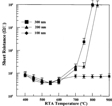
Figure 3. The sheet resistance of Ni-silicide formed on 100, 200, and 300
nm thick polysilicon with various silicidation temperatures.
Figure 4. XRD profiles of the Ni-silicide formed at 800°C on 100, 200, and
300 nm thick polysilicon films.
Journal of The Electrochemical Society, 148共9兲 G530-G533 共2001兲 G531
) unless CC License in place (see abstract). ecsdl.org/site/terms_use
address. Redistribution subject to ECS terms of use (see 140.113.38.11
agglomeration of the Ni-silicide; therefore, the surface energy of the mono-oriented grains could suppress the agglomeration of the Ni-silicide.
Moreover, the structure containing the film stack has superior thermal stability than that of the S or A samples, which could be further explained using the results demonstrated in Fig. 3-5.
The figures also show that the thermal stability of D is higher than that of c-Si above 850°C, although that of D is lower than that of c-Si under 800°C. This could be explained by the XRD data and the results presented in Fig. 3. For the D sample is mono-oriented poly-Si grains and the c-Si is single-crystalline silicon, the agglom-erating temperature could be higher for the c-Si sample. However, after agglomeration the D sample has better thermal stability be-cause the thinner poly-Si films have better thermal stability as shown in Fig. 3.
Figure 3 shows the average and error bars extracted from 20 points of measured sheet resistance of the Ni-silicide formed on polysilicon film with various thicknesses. It can be seen that the thinner the polysilicon film, the higher is the thermal stability of Ni-silicide. The underlying layer of silicon film with less thickness could suppress Ni-silicide agglomeration. This interpretation is sup-ported by the XRD profiles in terms that indicate the 300 nm film stack has strong NiSi2具311典 phase and this orientation is not found in the 100 nm sample as shown in Fig. 4 after 800°C 30 s RTA treatment. However, the NiSi2具311典 phase is also shown in the 200 nm sample, but it is much weaker than the 300 nm one. These NiSi2 grains with different orientation should be the main reason that makes Ni-silicide discontinuous and sheet resistance greater.
Figure 5 shows the TEM images of共a兲 DS, 共b兲 DA, and 共c兲 S samples. These samples are silicided by RTA at 800°C for 30 s. Figure 5. TEM images of the Ni-silicide formed at 800°C on共a兲 DS silicon
film, and共b兲 DA silicon film, and 共c兲 S silicon film.
Figure 6. SIMS profiles of the Ni-silicide formed at 800°C on S, D, DS, and
DA films.
Figure 7. Weibull plot of Ebdof the MOS capacitors with Ni-silicide gates formed at 800°C on S, D, A, DS, and DA silicon films.
Figure 8. Weibull plot of Qbdof the MOS capacitors with Ni-silicide gates formed at 800°C on S, D, A, DS, and DA silicon films.
Journal of The Electrochemical Society, 148共9兲 G530-G533 共2001兲
G532
) unless CC License in place (see abstract). ecsdl.org/site/terms_use
address. Redistribution subject to ECS terms of use (see 140.113.38.11
Ni-silicide extends mainly within the upper layer of silicon film for double-layer structures. Ni-silicide extends through the entire film for S sample. These results explain why samples with film stack structure have better thermal stability than S and A samples do. That is, Ni-silicide agglomeration of the stacked samples mainly occurred in the upper silicon film. According to the result shown in Fig. 3, the stacked films would have better thermal stability.
Figure 6 shows the SIMS profiles of the Ni-silicide formed on S, D, DS, and DA samples. All samples are silicided by RTA at 800°C for 30 s. We can find that the stacked samples have a much sharper profile than either the S or D sample. This indicates that the struc-tures of the film stack could suppress Ni penetration with the assis-tance of polysilicon films; therefore, these structures improve the reliability of the gate oxide. The mechanism of suppression could be attributed to the fact that Ni molecules are trapped as they migrate through the interface of the film stack. This phenomenon is similar to the occurrence reported by Wu et al. describing the boron pen-etration suppressed by stacked gate structure.8 These profiles also support that the Ni-silicide was formed only in the upper layer of the stacked film.
Figures 7 and 8 show the Weibull plots of breakdown electric field Ebdand charge to breakdown Qbddistributions for S, D, A, DS, and DA Ni-silicide gate MOS capacitors with the gate oxide thick-ness being 10 nm and the silicidation temperature processed at 800°C. These plots obtained here indicate that the stacked samples have higher Ebd and Qbd distributions than those of nonstacked samples. This may arise from the results presented in the Fig. 6 that the stacked gate structures suppress Ni penetration into oxides.
Conclusions
The Ni-silicide formed on stacked polysilicon gates is attractive in fabricating gates of MOS capacitors. Devices using gate
struc-tures proposed here can acquire better thermal stability and higher electrical reliability; that is, the samples could maintain low resis-tance, high Ebdand high Qbddistributions with 800°C RTA silicid-ation. In this paper, we also demonstrated the mechanism relating to these improvements.
Acknowledgment
This work is supported by 89-2215-E-009-036 and NSC-89-2215-E-009-030.
National Chiao Tung University assisted in meeting the publication costs of this article.
References
1. J. B. Lasky, J. S. Nakos, O. J. Cain, and P. J. Geiss, IEEE Trans. Electron Devices,
ED-38, 262共1991兲.
2. C. Y. Ting, F. M. d’Heurle, S. S. Iyer, and P. M. Fryer, J. Electrochem. Soc., 133, 2621共1986兲.
3. J. F. Chen and L. J. Chen, Thin Solid Films, 293, 34共1997兲.
4. S. A. Jang, T. K. Kim, I. S. Yeo, H. S. Kim, and S. K. Lee, IEEE Trans. Electron
Devices, ED-46, 2353共1999兲.
5. R. Mukai, S. Ozawa, and H. Yagi, Thin Solid Films, 270, 567共1995兲. 6. R. K. Shukla and J. S. Multani, in Proceeding of the Fourth VLSI Multilevel
Interconnection Conference, 470共1987兲.
7. S. Pramanick, B. K. Patnaik, and G. A. Rozgonyi, Mater. Res. Soc. Symp. Proc.,
309, 475共1993兲.
8. S. L. Wu, C. L. Lee, and T. F. Lei, IEEE Electron Device Lett., ED-15, 160共1994兲. 9. S. Hasegawa, S. Sakamoto, T. Inokuma, and Y. Kurata, Appl. Phys. Lett., 62共11兲, 15
共1993兲.
10. E. G. Lee and J. J. Kim, Thin Solid Films, 226, 123共1993兲. 11. Y. Wada and S. Nishimatsu, J. Electrochem. Soc., 125, 1499共1978兲. 12. B. A. Joece and R. R. Bradley, J. Electrochem. Soc., 110, 1235共1963兲.
Journal of The Electrochemical Society, 148共9兲 G530-G533 共2001兲 G533
) unless CC License in place (see abstract). ecsdl.org/site/terms_use
address. Redistribution subject to ECS terms of use (see 140.113.38.11